

Page 1

ADM6996F
6 port 10/100 Mb/s
Single Chip Ethernet Switch Controller
Data Sheet
V1.0
ADMtek.com.tw
Information in this document is provided in connection with ADMtek products. ADMtek may make
changes to specifications and product descriptions at an y time, without notice. Designers must not rely on
the absence or characteristics of any features or instructions marked “reserved” or “undefined”. ADMtek
reserves these for future definition and shall have no responsibility whatsoever for conflicts or
incompatibilities arising from future changes to them
The products may contain design defects or errors known as errata, which may cause the produ ct to deviate
from published specifications. Current characterized errata are available on request. To obtain latest
documentation please contact you local ADMtek sales office or visit ADMtek’s website at
http://www.ADMtek.com.tw
*Third-party brands and names are the property of their respective owners.
Copyright 2003 by ADMtek Incorporated All Rights Reserved.
Page 2

. V1.0
About this Manual
General Release
Intended Audience
ADMtek’s Customers
Structure
This Data sheet contains 6 chapters
Chapter 1 Product Overview
Chapter 2 Interface Description
Chapter 3 Function Description
Chapter 4. Register Description
Chapter 5. Electrical Specification
Chapter 6. Packaging
Revision History
Date Version Change
07 October 2003
1.0 1. First release of ADM6996F
Customer Support
ADMtek Incorporated,
2F, No.2, Li-Hsin Rd.,
Science-based Industrial Park,
Hsinchu, 300, Taiwan, R.O.C.
Sales Information
Tel + 886-3-5788879
Fax + 886-3-5788871
Page 3

. V1.0
Table of Contents
Chapter 1 Product Overview........................................................................................1-1
1.1 Overview..........................................................................................................1-1
1.2 Features............................................................................................................1-2
1.3 Applications.....................................................................................................1-2
1.4 Block Diagram.................................................................................................1-3
1.5 Abbreviations...................................................................................................1-3
1.6 Conventions .....................................................................................................1-5
1.6.1 Data Lengths............................................................................................1-5
1.6.2 Pin Types..................................................................................................1-5
1.6.2 Register Types..........................................................................................1-5
Chapter 2 Interface Description...................................................................................2-1
2.1 Pin Diagram.....................................................................................................2-1
2.2 Pin Description by Function ............................................................................2-2
2.2.1 Twisted Pair Interface..............................................................................2-2
2.2.2 5th Port (MII) Interfaces..........................................................................2-2
2.2.3 6th Port (MII) Interfaces..........................................................................2-3
2.2.4 LED Interface...........................................................................................2-5
2.2.5 EEPROM/Management Interface............................................................2-6
2.2.6 Power/Ground, 48 pins............................................................................2-6
2.2.7 Miscellaneous ..........................................................................................2-6
Chapter 3 Function Description...................................................................................3-1
3.1 Functional Descriptions...................................................................................3-1
3.2 10/100M PHY Block .......................................................................................3-1
3.3 100Base-X Module..........................................................................................3-1
3.4 100Base-X Receiver ........................................................................................3-2
3.4.1 A/D Converter..........................................................................................3-3
3.4.2 Adaptive Equalizer and timing Recovery Module ...................................3-3
3.4.3 NRZI/NRZ and Serial/Parallel Decoder..................................................3-3
3.4.4 Data De-scrambling.................................................................................3-3
3.4.5 Symbol Alignment ....................................................................................3-3
3.4.6 Symbol Decoding.....................................................................................3-4
3.4.7 Valid Data Signal.....................................................................................3-4
3.4.8 Receive Errors .........................................................................................3-4
3.4.9 100Base-X Link Monitor..........................................................................3-4
3.4.10 Carrier Sense...........................................................................................3-5
3.4.11 Bad SSD Detection...................................................................................3-5
3.4.12 Far-End Fault..........................................................................................3-5
3.5 100Base-TX Transceiver.................................................................................3-5
3.5.1 Transmit Drivers......................................................................................3-6
3.5.2 Twisted-Pair Receiver..............................................................................3-6
3.6 10Base-T Module.............................................................................................3-6
3.6.1 Operation Modes .....................................................................................3-6
3.6.2 Manchester Encoder/Decoder.................................................................3-7
3.6.3 Transmit Driver and Receiver .................................................................3-7
3.6.4 Smart Squelch ..........................................................................................3-7
ADM6996F i
Page 4

. V1.0
3.7 Carrier Sense....................................................................................................3-8
3.8 Jabber Function................................................................................................3-8
3.9 Link Test Function...........................................................................................3-8
3.10 Automatic Link Polarity Detection..............................................................3-8
3.11 Clock Synthesizer ........................................................................................3-8
3.12 Auto Negotiation..........................................................................................3-8
3.13 Memory Block.............................................................................................3-9
3.14 Switch Functional Description.....................................................................3-9
3.15 Basic Operation............................................................................................3-9
3.15.1 Address Learning...................................................................................3-10
3.15.2 Address Recognition and Packet Forwarding.......................................3-10
3.15.3 Address Aging........................................................................................3-11
3.15.4 Back off Algorithm.................................................................................3-11
3.15.5 Inter-Packet Gap (IPG) .........................................................................3-11
3.15.6 Illegal Frames........................................................................................3-11
3.15.7 Half Duplex Flow Control.....................................................................3-11
3.15.8 Full Duplex Flow Control......................................................................3-12
3.15.9 Broadcast Storm filter............................................................................3-12
3.16 Auto TP MDIX function................................................................................3-12
3.17 Port Locking...............................................................................................3-12
3.18 VLAN setting & Tag/Untag & port-base VLAN ......................................3-13
3.19 Priority Setting...........................................................................................3-14
3.20 LED Display ..............................................................................................3-14
Chapter 4 Register Description ....................................................................................4-1
4.1 EEPROM Content............................................................................................4-1
4.2 EEPROM Register Map...................................................................................4-1
4.3 EEPROM Register...........................................................................................4-2
4.3.1 Signature Register, offset: 0x00h..............................................................4-2
4.3.2 Configuration Registers, offset: 0x01h ~ 0x09h......................................4-3
4.3.3 Reserved Register, offset: 0x0ah..............................................................4-3
4.3.4 Configuration Register, offset: 0x0bh......................................................4-4
4.3.5 Reserved Register, offset: 0x0ch~0x0dh..................................................4-4
4.3.6 VLAN priority Map Register, offset: 0x0eh .............................................4-4
4.3.7 TOS priority Map Register, offset: 0x0fh.................................................4-4
4.3.8 Packet with Priority: Normal packet content ..........................................4-5
4.3.9 VLAN Packet............................................................................................4-5
4.3.10 TOS IP Packet..........................................................................................4-1
4.3.11 Miscellaneous Configuration Register, offset: 0x10h..............................4-1
4.3.12 VLAN mode select Register, offset: 0x11h...............................................4-2
4.3.13 Miscellaneous Configuration register, offset: 0x12h ..............................4-4
4.3.14 VLAN mapping table registers, offset: 0x22h ~ 0x13h............................4-4
4.3.15 Reserved Register, offset: 0x27h ~ 0x23h................................................4-4
4.3.16 Port0, 1 PVID bit 11 ~ 4 Configuration Register, offset: 0x28h.............4-1
4.3.17 Port2, 3 PVID bit 11 ~ 4 Configuration Register, offset: 0x29h.............4-1
4.3.18 Port4, 5 PVID bit 11~4 Configuration Register, offset: 0x2ah...............4-1
4.3.19 Port6, 7 PVID bit 11~4 Configuration Register, offset: 0x2bh...............4-1
ADM6996F ii
Page 5

. V1.0
4.3.20 Port8 PVID bit 11~4 & VLAN group shift bits Configuration Register..4-1
4.3.21 Reserved Register, offset: 0x2dh..............................................................4-2
4.3.22 Reserved Register, offset: 0x2eh..............................................................4-2
4.3.23 PHY Restart, offset: 0x2fh........................................................................4-2
4.3.24 Miscellaneous Configuration Register, offset: 0x30h..............................4-2
4.3.25 Bandwidth Control Register0~3, offset: 0x31h........................................4-3
4.3.26 Bandwidth Control Register 4~5, offset: 0x32h.......................................4-3
4.3.27 Bandwidth Control Enable Register, offset: 0x33h..................................4-4
4.4 EEPROM Access.............................................................................................4-4
4.5 Serial Register Map..........................................................................................4-6
4.6 Serial Register Description..............................................................................4-7
4.6.1 Chip Identifier Register, offset: 0x00h.....................................................4-7
4.6.2 Port Status 0 Register, offset: 0x01h .......................................................4-7
4.6.3 Port Status 1 Register, offset: 0x02h .......................................................4-9
4.6.4 Cable Broken Status Register, offset: 0x03h............................................4-9
4.6.5 Over Flow Flag 0 Register, offset: 0x3ah..............................................4-10
4.6.6 Over Flow Flag 0: Register 0x3bh ........................................................4-10
4.6.7 Over Flow Flag 2 Register, offset: 0x3ch..............................................4-11
4.7 Serial Interface Timing....................................................................................4-1
4.8 PHY Register Description................................................................................4-2
4.8.1 Control Register, offset: 0x00..................................................................4-2
4.8.2 Status Register, offset: 0x01.....................................................................4-4
4.8.3 PHY Identifier Register, offset: 0x02.......................................................4-5
4.8.4 PHY Identifier Register, offset: 0x03.......................................................4-5
4.8.5 Auto Negotiation Advertisement Register, offset : 0x04..........................4-6
4.8.6 Auto Negotiation Link Partner Ability Register, offset: 0x05..................4-7
4.8.7 Auto Negotiation Expansion Register, offset: 0x06.................................4-7
4.8.8 Next Page Transmit Register, offset: 0x07 .............................................4-8
4.8.9 Link Partner Next Page Register, offset: 0x08 ........................................4-8
Chapter 5 Electrical Specification................................................................................5-1
5.1 TX/FX Interface...............................................................................................5-1
5.1.1 TP Interface .............................................................................................5-1
5.1.2 FX Interface.............................................................................................5-1
5.2 DC Characteristics...........................................................................................5-2
5.2.1 Absolute Maximum Rating.......................................................................5-2
5.2.2 Recommended Operating Conditions......................................................5-2
5.2.3 DC Electrical Characteristics for 3.3V Operation..................................5-2
5.3 AC Characteristics...........................................................................................5-3
5.3.1 Power On Reset........................................................................................5-3
5.3.2 EEPROM Interface Timing......................................................................5-3
5.3.3 10Base-TX MII Input Timing...................................................................5-4
5.3.4 10Base-TX MII Output Timing ................................................................5-4
5.3.5 100Base-TX MII Input Timing.................................................................5-5
5.3.6 100Base-TX MII Output Timing ..............................................................5-5
5.3.7 SMI Timing...............................................................................................5-6
5.3.8 GPSI(7-wire) Input Timing......................................................................5-6
ADM6996F iii
Page 6

. V1.0
5.3.9 GPSI(7-wire) Output Timing ...................................................................5-7
5.3.10 Serial Management Interface (MDC/MDIO) Timing..............................5-8
Chapter 6 Packaging......................................................................................................6-1
6.1 128 Pin PQFP Outside Dimension...................................................................6-1
ADM6996F iv
Page 7

. V1.0
List of Figures
Figure 1-1 ADM6996F Block Diagram...........................................................................1-3
Figure 2-1 4 TP/FX PORT + 2 MII PORT 128 Pin Diagram..........................................2-1
ADM6996F v
Page 8

ADM6996F Product Review
Chapter 1 Product Overview
1.1 Overview
The ADM6996F is a high performance, low cost, highly integrated (Controller, PHY and
Memory) four-port 10/100 Mbps TX/FX plus two 10/100 MAC port Ethernet switch
controller with all ports supporting 10/100 Mbps Full/Half duplex. The ADM6996F is
intended for applications to stand alone bridge for low cost SOHO markets such as 5Port,
Router applications. The 2
integrated.
ADM6996F provides the most advance functions such as: 802.1p(Q.O.S.),
802.1q(VLAN), Port MAC address Locking, Management, Port Status, TP AutoMDIX, 25M Crystal & Extra MII port functions to meet customer requests on Switch
demand.
The ADM6996F also supports Back Pressure in Half-Duplex mode and 802.3x Flow
Control Pause packet in Full-Duplex mode to prevent packet loss when buffers are full.
When Back Pressure is enabled, and there is no receive buffer available for the incoming
packet, the ADM6996F will issue a JAM pattern on the receiving port in Half Duplex
mode and transmit the 802.3x Pause packet back to receiving end in Full Duplex mode.
The built-in SRAM used for the packet buffer and address learning table is divided into
256 bytes/block to achieve the optimized memory utilization through complicated link
list on packets with various lengths.
ADM6996F also supports priority features by Port-Base, VLAN and IP TOS field
checking. Users can easily set different priority modes in individual ports, through a
small low-cost micro controller to initialize or on-the-fly to configure. Each output port
supports four queues in the way of fixed N: 1 fairness queuing to fit the bandwidth
demand on various types of packet such as Voice, Video and data. 802.1Q, Tag/Untag,
and up to 16 groups of VLAN are also supported.
An intelligent address recognition algorithm allows ADM6996F to recognize up to 2048
different MAC addresses and enables filtering and forwarding at full wire speed.
Port MAC address Locking function is also supported by ADM6996F to use on Building
Internet access to prevent multiple users sharing one port traffic.
nd
MAC can be configured as PCS type MII with 10/100 PHY
ADMtek Inc. 1-1
Page 9

ADM6996F Product Review
1.2 Features
• Supports four 10M/100M auto-detect Half/Full duplex switch ports with TX/FX
interfaces and two MII/GPSI ports.
• Supports 2048 MAC addresses table.
• Supports four queue for QoS
• Supports priority features by Port-Based, 802.1p VLAN & IP TOS of packets.
• Supports Store & Forward architecture and performs forwarding and filtering at non-
blocking full wire speed.
• Supports buffer allocation with 256 bytes per block
• Supports Aging function Enable/Disable.
• Supports per port Single/Dual color mode with Power On auto diagnostic.
• Supports 802.3x Flow Control pause packet for Full Duplex in case buffer is full.
• Supports Back Pressure function for Half Duplex operation in case buffer is full.
• Supports packet lengths up to 1522 bytes.
• Broadcast Storming Filter function.
• Supports 802.1Q VLAN. Up to 16 VLAN groups are implemented by the last four
bits of VLAN ID.
• 2bit MAC clone to support multiple WAN application
• Supports TP interface Auto MDIX function for auto TX/RX swap by strapping-pin.
• Easy Management 32bits smart counter for per port RX/TX byte/packet count, error
count and collision count.
• Supports PHY status output for management system.
• 25M Crystal only for the whole system.
• 128 QFP package with 0.18um technology. 1.8V/3.3V power supply.
1.3 Applications
ADM6996F in 128-pin PQFP: SOHO 5-port switch
5-port switch + Router with MII CPU interface.
ADMtek Inc. 1-2
Page 10
ADM6996F Product Review
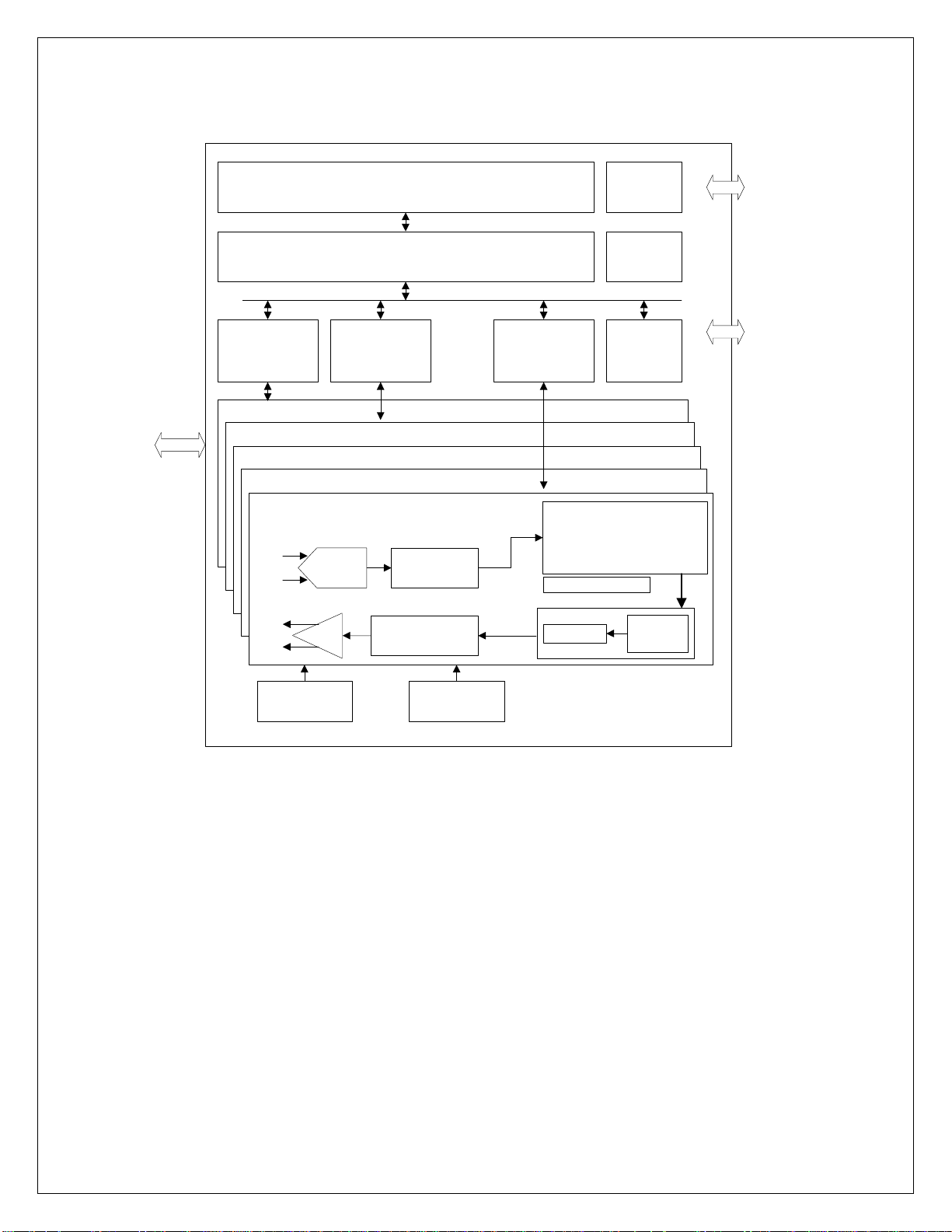
1.4 Block Diagram
Twisted
Pai r
Interface
10/100M
MAC
RXP4
RXN 4
TXP4
TXN4
A/D
CONV ERTER
DRIVER
Embedded Memory
Switching Fabric
10/100M
MAC
PORT 0
PORT 1
PORT2
...
PORT N
DIGITAL
EQUALIZER
MLT3 Converter
...
10/100M
MAC
PARTITION HANDLER
SCRAMBLER
LED
DISPLAY
CONTROL
Memory
BIST
10/100M
MAC
Data Handler
TRANSMIT
STATE
MACHINE
LED
Interface
MII
Interface
1.5 Abbreviations
BER Bit Error Rate
CFI Canonical Format Indicator
COL Collision
CRC Cyclic Redundancy Check
CRS Carrier Sense
CS Chip Select
DA Destination Address
DI Data Input
DO Data Output
EDI EEPROM Data Input
EDO EEPROM Data Output
EECS EEPROM Chip Select
CLOCK GENERATORBIAS
Figure 1-1 ADM6996F Block Diagram
ADMtek Inc. 1-3
Page 11

ADM6996F Product Review
EESK EEPROM Clock
ESD End of Stream Delimiter
FEFI Far End Fault Indication
FET Field Effect Transistor
FLP Fast Link Pulse
GND Ground
GPSI General Purpose Serial Interface
IPG Inter-Packet Gap
LFSR Linear Feedback Shift Register
MAC Media Access Controller
MDIX MDI Crossover
MII Media Independent Interface
NRZI Non Return to Zero Inverter
NRZ Non Return to Zero
PCS Physical Coding Sub-layer
PHY Physical Layer
PLL Phase Lock Loop
PMA Physical Medium Attachment
PMD Physical Medium Dependent
QoS Quality of Service
QFP Quad Flat Package
RST Reset
RXCLK Receive Clock
RXD Receive Data
RXDV Receive Data Valid
RXER Receive Data Errors
RXN Receive Negative (Analog receive differential signal)
RXP Receive Positive (Analog receive differential signal)
SA Source Address
SOHO Small Office Home Office
SSD Start of Stream Delimiter
SQE Signal Quality Error
TOS Type of Service
TP Twisted Pair
TTL Transistor Transistor Logic
TXCLK Transmission Clock
TXD Transmission Data
TXEN Transmission Enable
TXN Transmission Negative
TXP Transmission Positive
ADMtek Inc. 1-4
Page 12

ADM6996F Product Review
1.6 Conventions
1.6.1 Data Lengths
qword 64-bits
dword 32-bits
word 16-bits
byte 8 bits
nibble 4 bits
1.6.2 Pin Types
Pin Type Description
I Input
O Output
I/O Bi-directional
OD Open drain
SCHE Schmitt Trigger
PD internal pull-down
PU internal pull-up
1.6.2 Register Types
Register Type Description
RO Read-only
WO Write-only
RW Read/Write
ADMtek Inc. 1-5
Page 13
ADM6996F Interface Description
Chapter 2 Interface Description
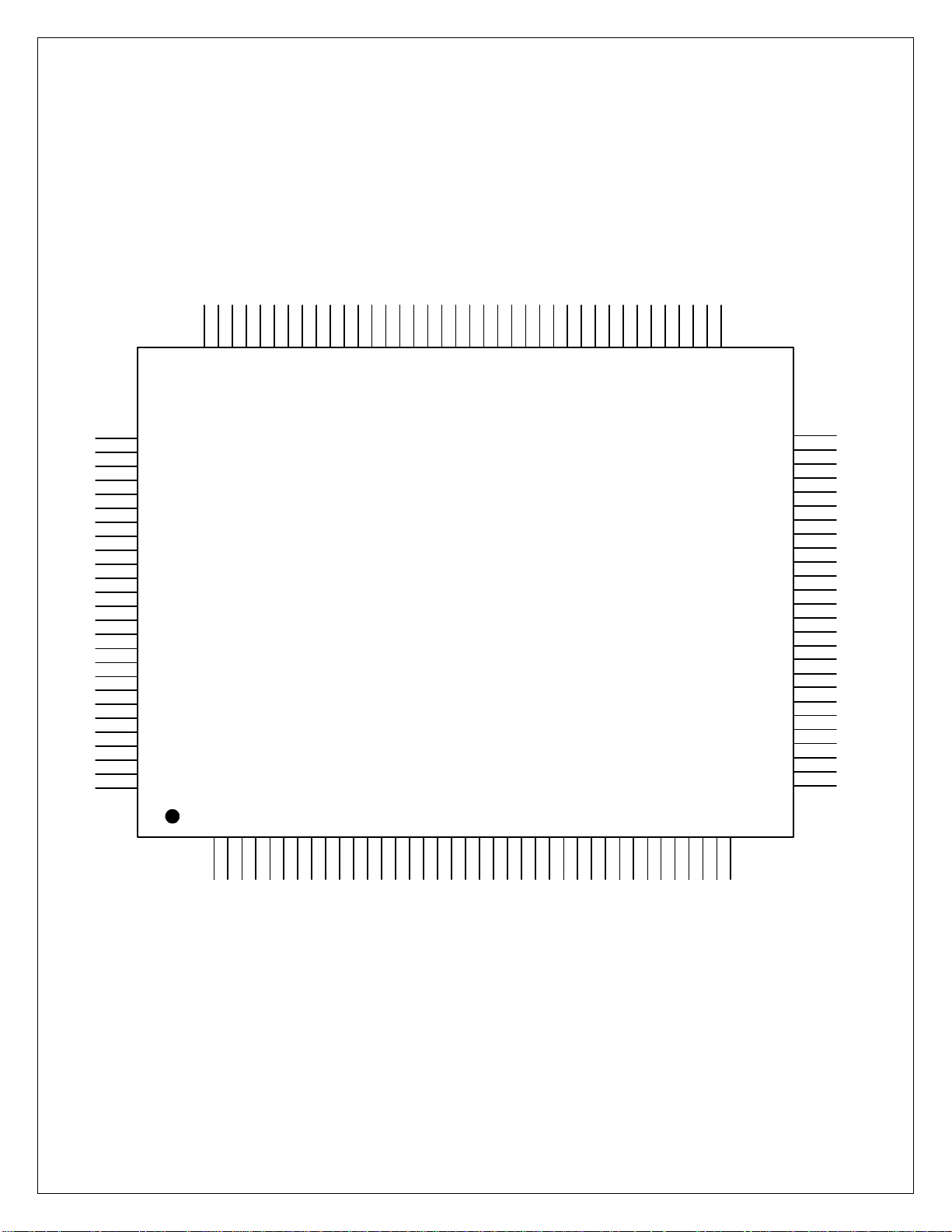
2.1 Pin Diagram
100
101
102
P4RXD3
P4RXD2
P4RXD1
99
LNKACT0
GNDO
97
98
LNKACT1
95
96
VCC2IK
LNKACT3
LNKACT2
72
73
74
75
76
77
78
79
80
81
82
83
84
85
86
87
88
89
90
91
92
93
94
P5RXCLK
P4RXDV
P4RXD0
VCC2IK
GNDIK
P4CRS
P4COL
EDI (DUAL COLOR)
EECS
EESK (XOVEN)
VCC2IK
GNDIK
EDO
CKO25M
CFG0
GNDO
VCC3O
SPDTNP5
LNKFP5
DPHALFP5
LNKFP4
GNDIK
70
71
GNDO
VCC3O
69
P5RXER
GNDO
68
P5TXCLK
676665
VCC2IK
P5TXEN(PHYAS0)
103
P4TXD3
104
P4TXD2
105
P4TXD1 (P4TYPE1)
106
P4TXD0 (P4TYPE0)
107
DPHALFP4
108
GNDO
109
VCC3O
110
DUPCOL3
111
DUPCOL2 (RECBPEN)
112
DUPCOL1(PHYAS1)
113
DUPCOL0(RECANEN)
114
P4TXEN
115
P4TXCLK
116
VCCIK
117
P4RXCLK
118
GNDIK
119
RC
120
XI
121
XO
122
VCCPLL
123
GNDPLL
124
CONTROL
125
VREF
126
GNDBIAS
127
RTX
128
VCCBIAS
VCCA2
TXP0
234
1
TXN0
GNDA
GNDA
5
RXN0
RXP0
678
ADM6996F
VCCAD
VCCA2
GNDA
TXN1
TXP1
101112131415161718192021222324252627282930
9
GNDA
RXP1
RXN1
VCCAD
VCCA2
TXN2
TXP2
GNDA
RXP2
RXN2
VCCAD
VCCA2
TXP3
TXN3
GNDA
GNDA
VCCAD
RXN4
RXN3
RXP3
31323334353637
RXP4
GNDA
GNDA
(GFCEN) P5TXD0
(P5GPSI) P5TXD1
P5TXD2
P5TXD3
P5COL
P5RXD3
P5RXD2
P5RXD1
P5RXD0
P5RXDV
SPDTNP4
GNDO
VCC3O
LDSPD3
LDSPD2
LDSPD1
LDSPD0
P4RXER
VCCA2
TXN4
TXP4
38
GNDIK
P4FX
P5CRS
VCCIK
GNDIK
MDC
TEST
MDIO
64
63
62
61
60
59
58
57
56
55
54
53
52
51
50
49
48
47
46
45
44
43
42
41
40
39
Figure 2-1 4 TP/FX PORT + 2 MII PORT 128 Pin Diagram
ADMtek Inc. 2-1
Page 14

ADM6996F Interface Description
2.2 Pin Description by Function
ADM6996F pins are categorized into one of the following groups:
Section 2.2.1 Twisted Pair Interface
Section 2.2.2 5th Port (MII) Interfaces
Section 2.2.3 6th Port (MII) Interfaces
Section 2.2.4 LED Interface
Section 2.2.5 EEPROM/Management Interface
Section 2.2.6 Power/Ground, 48 pins
Section 2.2.7 Miscellaneous
Note:
“Section 1.6.2 Pin Types” can be used for reference.
2.2.1 Twisted Pair Interface
Pin Name Pin# Type Descriptions
RXP[0:4] 6, 14, 21, 29, 33 I/O,
Analog
RXN[0:4] 7, 15, 22, 30, 32 I/O,
Analog
TXP[0:4] 2, 10, 18, 25, 37 I/O,
Analog
TXN[0:4] 3, 11, 19, 26, 36 I/O,
Analog
Twisted Pair Receive Input Positive.
Twisted Pair Receive Input Negative.
Twisted Pair Transmit Output Positive.
Twisted Pair Transmit Output Negative.
2.2.2 5th Port (MII) Interfaces
Pin Name Pin# Type Descriptions
P4TXD[0]
Setting
P4TYPE0
P4TXD[1]
Setting
P4TYPE1
P4TXD[3:2] 103, 104 I/O,
106 I/O,
8mA
PD
105 I/O,
8mA
PD
8mA
PD
Port4 MII transmit data 0
Acts as MII transmit data TXD[0]. Synchronous to the rising
edge of TXCLK.
Setting
P4TYPE0 : At power-on-reset, latched as P4 TYPE0.
Port4 MII Transmit Data bit 1
Synchronous to the rising edge of TXCLK. These pins act
as MII TXD[1].
Setting
P4TYPE1 : At power-on-reset, latched as P4 TYPE1.
Port4 MII Transmit Data bit 3~2
Synchronous to the rising edge of TXCLK. These pins act
as MII TXD[3:2].
ADMtek Inc. 2-2
Page 15

ADM6996F Interface Description
Pin Name Pin# Type Descriptions
P4FX 62 I
PD
Port4 FX/TX mode select. Internal pull down.
1: Port4 as FX port.
0: Port4 as TX port.
P4TXEN
P4RXD[0] 74 I
P4RXD[3:1] 102, 101,
P4RXDV 73 I
P4RXER 39 I
P4COL 78 I
P4CRS 77 I
P4RXCLK 117 I
P4TXCLK 115 I
DHALFP4 107 I
LNKFP4 92 I
SPDTNP4 51 I
114 I/O
8mA
PD
PD
100
PD
PD
PD
PD
PD
PD
PD
PD
PD
PD
Port4 MII Transmit Enable. Internal pull down.
Port4 MII port receive data 0
These pins act as MII RXD[0]. Synchronous to the rising
edge of P4RXCLK. Internal pull down.
I
Port4 MII port receive data 3~0
These pins act as MII RXD[3:0]. Synchronous to the rising
edge of P4RXCLK. Internal pull down.
Port4 MII receive data valid.
Internal pull down.
Port4 MII Port Receive Error.
Internal pull down.
Port4 MII Port Collision input
Internal pull down.
Port4 MII Port Carrier Sense
Internal pull down.
Port4 MII Port Receive Clock Input
Port4 MII Port Transmit clock Input
Port4 MII Port Hardware Duplex input pin.
Low: Full Duplex. High: Half Duplex.
Internal pull down.
Port4 MII Port Hardware Link input pin.
Low: Link OK. High: Link Off.
Internal pull down.
Port4 MII Port Hardware Speed input pin.
Low: 100M. High: 10M.
Internal pull down.
2.2.3 6th Port (MII) Interfaces
Pin Name Pin# Type Descriptions
P5TXD[0]
Setting
GFCEN
63 I/O,
8mA
PU
MII transmit data 0 /GPSI TXD
Acts as MII transmit data TXD[0]. Synchronous to the rising
edge of TXCLK.
Setting
GFCEN: Global Flow Control Enable.
At power-on-reset, latched as Full Duplex Flow control
setting
ADMtek Inc. 2-3
Page 16

ADM6996F Interface Description
Pin Name Pin# Type Descriptions
“1” to enable flow-control (default ), “0” to disable flowcontrol.
P5TXD[1]
Setting
P5GPSI
P5TXD[3:2] 59, 60 I/O,
P5TXEN
Setting
PHYAS0
P5RXD[3:0] 56, 55, 54, 53 I
P5RXDV 52 I
P5RXER 68 I
P5COL 58 I
P5CRS 57 I
P5RXCLK 72 I
P5TXCLK 67 I
DHALFP5 91 I
61 I/O,
8mA
PD
8mA
PD
66 I/O
8mA
PD
PD
PD
PD
PD
PD
PD
PD
PD
MII Transmit Data bit 1
Synchronous to the rising edge of TXCLK. These pins act
as MII TXD[1].
Setting
P5GPSI: Port 5 GPSI Enable.
At power-on-reset, latched as P5 GPSI Enable.
“0” to disable port 5 GPSI (default ), “1” to enable port 5
GPSI.
Port5 MII Transmit Data bit 3~2
Synchronous to the rising edge of TXCLK. These pins act
as MII TXD[3:2].
Port5 MII Transmit Enable. Internal pull down.
Setting
PHYAS0: Chip physical address for multiple chip application
on read EEPROM data. Internal pull down.
Power on reset value PHYAS0 combines with PHYAS1
PHYAS1 PHYAS0
0 0 Master(93C46)
If there is no EEPROM then user must use 93C66 timing to
write chip’s register.
If user put 93C46 with correct Signature then user writes
chip register by 93C46 timing.
If user put 93C66 then data put in Bank0. User can write
chip register by 93C66 timing.
User must assert one SK cycle when CS at idle stage when
write chip internal register.
Port5 MII port receive data 3~0
These pins act as MII RXD[3:0]. Synchronous to the rising
edge of P5RXCLK. Internal pull down.
Port5 MII receive data valid.
Internal pull down.
Port5 MII Port Receive Error.
Internal pull down.
Port5 MII Port Collision input
Internal pull down.
Port5 MII Port Carrier Sense
Internal pull down.
Port5 MII Port Receive Clock Input
Port5 MII Port Transmit clock Input
Port5 MII Port Hardware Duplex input pin.
Low: Full Duplex. High: Half Duplex.
ADMtek Inc. 2-4
Page 17

ADM6996F Interface Description
Pin Name Pin# Type Descriptions
Internal pull down.
LNKFP5 90 I
PD
SPDTNP5 89 I
PD
Port5 MII Port Hardware Link input pin.
Low: Link OK. High: Link Off.
Internal pull down.
Port5 MII Port Hardware Speed input pin.
Low: 100M. High: 10M.
Internal pull down.
2.2.4 LED Interface
Pin Name Pin# Type Descriptions
LNKACT[3:0] 95,
96, 97,
98
DUPCOL[3] 110 O,
DUPCOL[2]
Setting
BPEN
DUPCOL[1]
Setting
PHYAS1
DUPCOL[0]
Setting
ANEN
LDSPD[3:0] 48, 47, 43, 42 O,
111 O,
112 O,
113 O,
O,
8mA
8mA
8mA,
PU
8mA,
PD
8mA,
PU
8mA
LINK/Activity LED[3:0]. Active low
“1” indicates no link activity on cable
“0” indicates link okay on cable, but no activity and signals
on idle stage.
“Blinking” indicates link activity on cable.
Duplex/Collision LED[3]. Active low
“1” for half-duplex and “blinking” for collision indication
“0” for full-duplex indication
Duplex/Collision LED[2]. Active low
“1” for half-duplex and “blinking” for collision indication
“0” for full-duplex indication
Setting
BPEN: At power-on-reset, latched as Back Pressure setting
“1” to enable Back-Pressure (defaulted), “0” to disable Back
Pressure.
At power-on-reset, latched as Back Pressure setting “1” to
enable Back-Pressure (defaulted), “0” to disable Back
Pressure.
Duplex/Collision LED[1]. Active low
“1” for half-duplex and “blinking” for collision indication
“0” for full-duplex indication
Setting
PHYAS1: Power on Reset latch value combine with TXEN.
Internal pull down. Check pin 66.
Duplex/Collision LED[0]. Active low
“1” for half-duplex and “blinking” for collision indication
“0” for full-duplex indication
Setting
ANEN: On power-on-reset, latched as Auto Negotiation
capability for all ports.
“1” to enable Auto Negotiation ( defaulted by pulled up
internally ),
“0” to disable Auto Negotiation.
Speed LED[3:0]. Used to indicate corresponding port’s
speed status. “0” for 100Mb/s, “1” for 10Mb/s
ADMtek Inc. 2-5
Page 18

ADM6996F Interface Description
2.2.5 EEPROM/Management Interface
Pin Name Pin# Type Descriptions
EDO 84 I,
TTL,PU
EECS 80 O,
4mA,PD
EECK
Setting
XOVEN
EDI
Setting
LEDMODE
81 I/O,
4mA
PD
79 I/O,
4mA
PD
EEPROM Data Output. Serial data input from EEPROM.
This pin is internally pull-up.
EEPROM Chip Select. This pin is active high chip enable
for EEPROM. When RESETL is low, it will be Tri-state.
Internally Pull-down
Serial Clock. This pin is clock source for EEPROM. When
RESETL is low, it will be tri-state.
Setting
XOVEN: This pin is internal pull-down. On power-on-reset,
latched as P4~0 Auto MDIX enable or not.
“0” to disable MDIX ( defaulted ), “1” to enable MDIX.
Suggest externally pull up to enable MDIX for all ports.
EEPROM Serial Data Input. This pin is output for serial
data transfer. When RESETL is low, it will be tri-state.
Setting
LEDMODE: This pin is internal pull-down. On power-onreset, latched as Dual Color mode or not.
“0” to set Single color mode for LED.
“1” to set Dual Color mode for LED.
2.2.6 Power/Ground, 48 pins
Pin Name Pin# Type Descriptions
GNDA 4,5,12, 13, 20, 27,
28, 34, 35
VCCA2 1, 9, 17, 24, 38 I 1.8V, Power Used by TX Line Driver.
VCCAD 8, 16, 23, 31 I 3.3V, Power Used by AD Block.
GNDBIAS 126 I Ground Used by Bias Block
VCCBIAS 128 I 3.3V, Power Used by Bias Block.
GNDPLL 123 I Ground used by PLL
VCCPLL 122 I 1.8V, Power used by PLL
GNDIK 45, 64, 76, 83, 93,
118
VCCIK 46, 65, 75, 82, 94,
116
GNDO 50, 69, 70, 87, 99,
108
VCC3O 49, 71, 88, 109 I 3.3V, Power Used by Digital Pad.
I Ground Used by AD Block.
I Ground Used by Digital Core
I 1.8V, Power Used by Digital Core
I Ground Used by Digital Pad
2.2.7 Miscellaneous
Pin Name Pin# Type Descriptions
CKO25M 85 O, 25M Clock Output.
ADMtek Inc. 2-6
Page 19

ADM6996F Interface Description
Pin Name Pin# Type Descriptions
8mA
Control 124 O
RTX 127 Analog TX Resistor. Add 1.1K %1 resister to GND.
VREF 125 Analog Analog Reference Voltage.
RC 119 I,
SCHE
XI 120 I,
Analog
XO 121 O,
Analog
CFG0 86 I,
PU
MDIO 40 I/O,
8mA
PU
MDC 44 I,
SCHE
TEST 41 I,
PD
FET Control Signal.
The pin is used to control FET for 3.3V to 1.8V regulator.
RC Input for Power On reset. Reset input pin.
25M Crystal Input. 25M Crystal Input. Variation is limited to
+/- 50ppm.
25M Crystal Output. When connected to oscillator, this pin
should left unconnected.
Configuration of Port 4 MII Mode
CFG0 P4TYPE Description
0 00 5 Port and 1 MII interface
0 01 4 Port and 2 MII(MAC) interface
1 xx 4 Port and 1 MII(MAC) and 1 MII(PCS)
Management Data. MDIO transfers management data in
and out of the device synchronous to MDC.
Management Data Reference Clock. A non-continuous
clock input for management usage. ADM7001/T will use
this clock to sample data input on MDIO and drive data onto
MDIO according to rising edge of this clock.
TEST Value.
At normal application connect to GND.
ADMtek Inc. 2-7
Page 20

ADM6996F Function Description
Chapter 3 Function Description
3.1 Functional Descriptions
The ADM6996F integrates four 100Base-X physical sub-layer (PHY), 100Base-TX
physical medium dependent (PMD) transceivers, four complete 10Base-T modules, 6
port 10/100 switch controller and two 10/100 MII/GPSI MAC and memory into a single
chip for both 10Mbits/s, 100Mbits/s Ethernet switch operation. It also supports 100BaseFX operation through external fiber-optic transceivers. The device is capable of operating
in either Full Duplex mode or Half-Duplex mode in 10Mbits/s and 100Mbits/s.
Operational modes can be selected by hardware configuration pins, software settings of
management registers, or determined by the on-chip auto negotiation logic.
The ADM6996F consists of three major blocks:
• 10/100M PHY Block
• Switch Controller Block
• Built-in SSRAM
The interfaces used for communication between PHY block and switch core is MII
interface.
Auto MDIX function is supported in this block. This function can be Enable/Disable by
hardware pin.
3.2 10/100M PHY Block
The 100Base-X section of the device implements the following functional blocks:
• 100Base-X physical coding sub-layer (PCS)
• 100Base-X physical medium attachment (PMA)
• Twisted-pair transceiver (PMD)
• The 100Base-X and 10Base-T sections share the following functional blocks.
• Clock synthesizer module
• MII Registers
• IEEE 802.3u auto negotiation
3.3 100Base-X Module
The ADM6996F implements 100Base-X compliant PCS and PMA and 100Base-TX
compliant TP-PMD as illustrated in Figure 2. Bypass options for each of the major
functional blocks within the 100Base-X PCS provides flexibility for various applications.
100Mbits/s PHY loop back is included for diagnostic purpose.
ADMtek Inc. 3-1
Page 21
ADM6996F Function Description
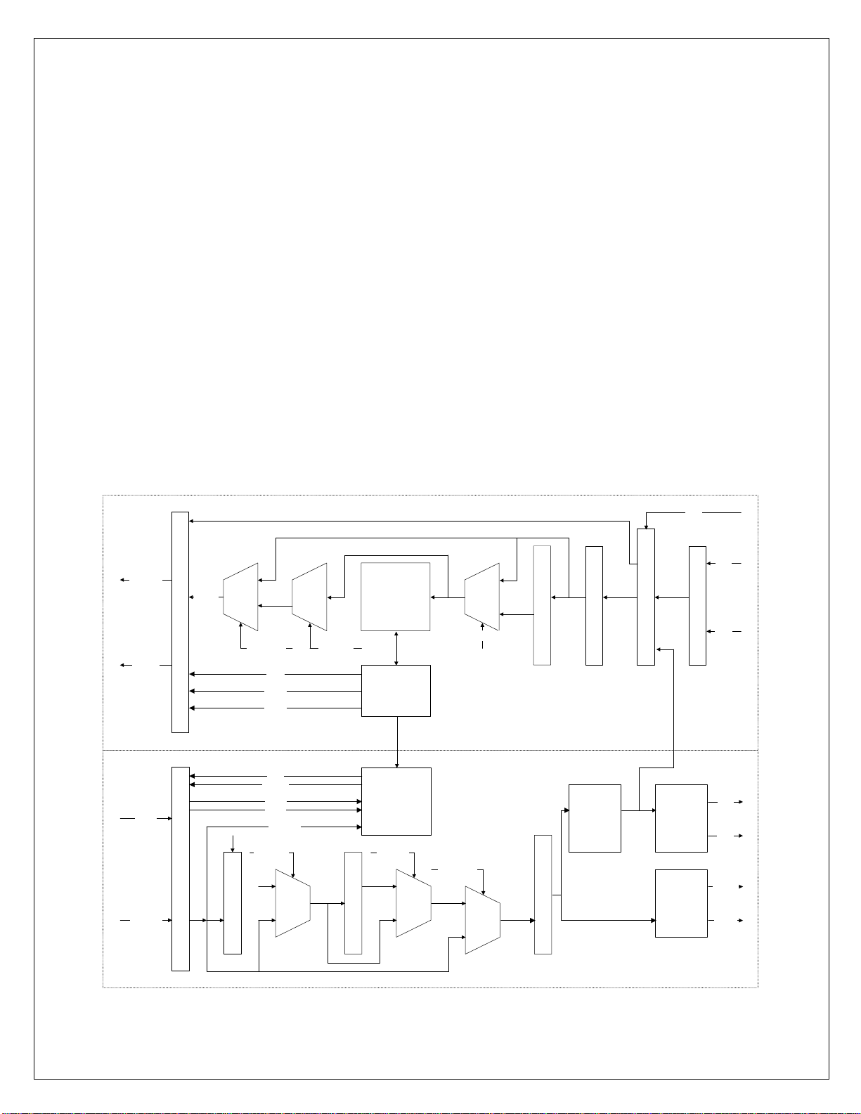
3.4 100Base-X Receiver
The 100Base-X receiver consists of functional blocks required to recover and condition
the 125Mbits/s receive data stream. The ADM6996F implements the 100Base-X
receiving state machine diagram as given in ANSI/IEEE Standard 802.3u, Clause 24. The
125Mbits/s receive data stream may originate from the on-chip twisted-pair transceiver in
a 100Base-TX application. Alternatively, the receive data stream may be generated by an
external optical receiver as in a 100Base-FX application.
The receiver block consists of the following functional sub-blocks :
• A/D Converter
• Adaptive Equalizer and timing recovery module
• NRZI/NRZ and serial/parallel decoder
• De-scrambler
• Symbol alignment block
• Symbol Decoder
• Collision Detect Block
• Carrier sense Block
• Stream decoder block
CLOCK/DATA RECOVERY
SDP
10/100
TX
DRIVER
FIBER
OPTIC
DRIVER
RXP
RXN
ADAPTIVE EQUALIZER
TXP
TXN
FOTX+
FOTX-
RXD[1:0]
CRSDV
TXEN
TXD[1:0]
MII TO RMII CONVERTER
RMII TO MII CONVERTER
RXD[3:0]
BP_ALIGN
CRS
RXDV
RXER
COL
TXCLK
TXEN
TXER
TXD[3:0]
BP_4B5B
4B/5B DECODER
BP_4B5B
4B/5B
DECODER
RX STATE
MACHINE
TX STATE
MACHINE
BP_SCR
SCRAMBLER
BP_DSCR
100BASE-X RECEIVER
BP_ALIGN
DESCRAMBLER
SERIAL-TO-PARALLEL
MLT-3
STATE
MACHINE
PARALLAL-TO-SERIAL
100BASE-X TRANSMITTER
ADMtek Inc. 3-2
Page 22

ADM6996F Function Description
3.4.1 A/D Converter
A high performance A/D converter with 125Mhz sampling rate converts signals received
on RXP/RXN pins to 6 bits data streams; it also possess auto-gain-control capabilities
that will further improve receive performance especially under long cable or harsh
detrimental signal integrity. Due to high pass characteristic on transformer, built in baseline-wander correcting circuit will cancel it out and restore its DC level.
3.4.2 Adaptive Equalizer and timing Recovery Module
All digital design is especially immune from noise environments and achieves better
correlation between production and system testing. Baud rate Adaptive Equalizer/Timing
Recovery compensates line loss induced from twisted pair and tracks far end clock at
125M samples per second. Adaptive Equalizer implemented with Feed forward and
Decision Feedback techniques meet the requirement of BER less than 10-12 for
transmission on CAT5 twisted pair cable ranging from 0 to 120 meters.
3.4.3 NRZI/NRZ and Serial/Parallel Decoder
The recovered data is converted from NRZI to NRZ. The data is not necessarily aligned
to 4B/5B code group’s boundary.
3.4.4 Data De-scrambling
The de-scrambler acquires synchronization with the data stream by recognizing idle
bursts of 40 or more bits and locking its deciphering Linear Feedback Shift Register
(LFSR) to the state of the scrambling LFSR. Upon achieving synchronization, the
incoming data is XORed by the deciphering LFSR and de-scrambled.
In order to maintain synchronization, the de-scrambler continuously monitors the validity
of the unscrambled data that it generates. To ensure this, a link state monitor and a hold
timer are used to constantly monitor the synchronization status. Upon synchronization of
the de-scrambler the hold timer starts a 722 us countdown. Upon detection of sufficient
idle symbols within the 722 us period, the hold timer will reset and begin a new
countdown. This monitoring operation will continue indefinitely given a properly
operating network connection with good signal integrity. If the link state monitor does
not recognize sufficient unscrambled idle symbols within 722 us period, the de-scrambler
will be forced out of the current state of synchronization and reset in order to re-acquire
synchronization.
3.4.5 Symbol Alignment
The symbol alignment circuit in the ADM6996F determines code word alignment by
recognizing the /J/K delimiter pair. This circuit operates on unaligned data from the descrambler. Once the /J/K symbol pair (11000 10001) is detected, subsequent data is
aligned on a fixed boundary.
ADMtek Inc. 3-3
Page 23

ADM6996F Function Description
3.4.6 Symbol Decoding
The symbol decoder functions as a look-up table that translates incoming 5B symbols
into 4B nibbles as shown in Table 1. The symbol decoder first detects the /J/K symbol
pair preceded by idle symbols and replaces the symbol with MAC preamble. All
subsequent 5B symbols are converted to the corresponding 4B nibbles for the duration of
the entire packet. This conversion ceases upon the detection of the /T/R symbol pair
denoting the end of stream delimiter (ESD). The translated data is presented on the
internal RXD[3:0] signal lines with RXD[0] represents the least significant bit of the
translated nibble.
3.4.7 Valid Data Signal
The valid data signal (RXDV) indicates that recovered and decoded nibbles are being
presented on the internal RXD[3:0] synchronous to receive clock, RXCLK. RXDV is
asserted when the first nibble of translated /J/K is ready for transfer over the internal MII.
It remains active until either the /T/R delimiter is recognized, link test indicates failure, or
no signal is detected. On any of these conditions, RXDV is de-asserted.
3.4.8 Receive Errors
The RXER signal is used to communicate receiver error conditions. While the receiver is
in a state of holding RXDV asserted, the RXER will be asserted for each code word that
does not map to a valid code-group.
3.4.9 100Base-X Link Monitor
The 100Base-X link monitor function allows the receiver to ensure that reliable data is
being received. Without reliable data reception, the link monitor will halt both transmit
and receive operations until such time that a valid link is detected.
The ADM6996F performs the link integrity test as outlined in IEEE 100Base-X (Clause
24) link monitor state diagram. The link status is multiplexed with 10Mbits/s link status
to form the reportable link status bit in serial management register 1h, and driven to the
LNKACT pin.
When persistent signal energy is detected on the network, the logic moves into a LinkReady state after approximately 500 us, and waits for an enable from the auto negotiation
module. When receive, the link-up state is entered, and the transmission and reception
logic blocks become active. Should auto negotiation be disabled, the link integrity logic
moves immediately to the link-up state after entering the link-ready state.
ADMtek Inc. 3-4
Page 24

ADM6996F Function Description
3.4.10 Carrier Sense
Carrier sense (CRS) for 100Mbits/s operation is asserted upon the detection of two
noncontiguous zeros occurring within any 10-bit boundary of the received data stream.
The carrier sense function is independent of symbol alignment. In switch mode, CRS is
asserted during either packet transmission or reception. For repeater mode, CRS is
asserted only during packet reception. When the idle symbol pair is detected in the
received data stream, CRS is de-asserted. In repeater mode, CRS is only asserted due to
receive activity. CRS is intended to encapsulate RXDV.
3.4.11 Bad SSD Detection
A bad start of stream delimiter (Bad SSD) is an error condition that occurs in the
100Base-X receiver if carrier is detected (CRS asserted) and a valid /J/K set of codegroup (SSD) is not received.
If this condition is detected, then the ADM6996F will assert RXER and present
RXD[3:0] = 1110 to the internal MII for the cycles hat correspond to received 5B codegroups until at least two idle code-groups are detected. Once at least two idle code groups
are detected, RXER and CRS become de-asserted.
3.4.12 Far-End Fault
Auto negotiation provides a mechanism for transferring information from the Local
Station to the link Partner that a remote fault has occurred for 100Base-TX. As auto
negotiation is not currently specified for operation over fiber, the far end fault indication
function (FEFI) provides this capability for 100Base-FX applications.
A remote fault is an error in the link that one station can detect while the other cannot. An
example of this is a disconnected wire at a station’s transmitter. This station will be
receiving valid data and detect that the link is good via the link integrity monitor, but will
not be able to detect that its transmission is not propagating to the other station.
A 100Base-FX station that detects such a remote fault may modify its transmitted idle
stream from all ones to a group of 84 ones followed by a single 0. This is referred to as
the FEFI idle pattern.
3.5 100Base-TX Transceiver
ADM6996F implements a TP-PMD compliant transceiver for 100Base-TX operation.
The differential transmit driver is shared by the 10Base-T and 100Base-TX subsystems.
This arrangement results in one device that uses the same external magnetic for both the
10Base-T and the 100Base-TX transmission with simple RC component connections.
The individually wave-shaped 10Base-T and 100Base-TX transmit signals are
multiplexed in the transmission output driver selection.
ADMtek Inc. 3-5
Page 25

ADM6996F Function Description
3.5.1 Transmit Drivers
The ADM6996F 100Base-TX transmission driver implements MLT-3 translation and
wave-shaping functions. The rise/fall time of the output signal is closely controlled to
conform to the target range specified in the ANSI TP-PMD standard.
3.5.2 Twisted-Pair Receiver
For 100Base-TX operation, the incoming signal is detected by the on-chip twisted-pair
receiver that consists of a differential line receiver, an adaptive equalizer and a base-line
wander compensation circuits.
The ADM6996F uses an adaptive equalizer that changes filter frequency response in
accordance with cable length. The cable length is estimated based on the incoming signal
strength. The equalizer tunes itself automatically for any cable length to compensate for
the amplitude and phase distortions incurred from the cable.
3.6 10Base-T Module
The 10Base-T Transceiver Module is IEEE 802.3 compliant. It includes the receiver,
transmitter, collision, heartbeat, loop back, jabber, wave shaper, and link integrity
functions, as defined in the standard. Figure 3 provides an overview for the 10Base-T
module.
The ADM6996F 10Base-T module is comprised of the following functional blocks:
• Manchester encoder and decoder
• Collision detector
• Link test function
• Transmit driver and receiver
• Serial and parallel interface
• Jabber and SQE test functions
• Polarity detection and correction
3.6.1 Operation Modes
The ADM6996F 10Base-T module is capable of operating in either half-duplex mode or
full-duplex mode. In half-duplex mode, the ADM6996F functions as an IEEE 802.3
compliant transceiver with fully integrated filtering. The COL signal is asserted during
collisions or jabber events, and the CRS signal is asserted during transmit and receive. In
full duplex mode the ADM6996F can simultaneously transmit and receive data.
ADMtek Inc. 3-6
Page 26

ADM6996F Function Description
3.6.2 Manchester Encoder/Decoder
Data encoding and transmission begins when the transmission enable input (TXEN) goes
high and continues as long as the transceiver is in good link state. Transmission ends
when the transmission enable input goes low. The last transition occurs at the center of
the bit cell if the last bit is a 1, or at the boundary of the bit cell if the last bit is 0.
Decoding is accomplished by a differential input receiver circuit and a phase-locked loop
that separate the Manchester-encoded data stream into clock signals and NRZ data. The
decoder detects the end of a frame when no more mid bit transitions are detected. Within
one and half bit times after the last bit, carrier sense is de-asserted.
3.6.3 Transmit Driver and Receiver
The ADM6996F integrates all the required signal conditioning functions in its 10Base-T
block such that external filters are not required. Only one isolation transformer and
impedance matching resistors are needed for the 10Base-T transmit and receive interface.
The internal transmit filtering ensures that all the harmonics in the transmission signal are
attenuated properly.
3.6.4 Smart Squelch
The smart squelch circuit is responsible for determining when valid data is present on the
differential receive. The ADM6996F implements an intelligent receive squelch on the
RXP/RXN differential inputs to ensure that impulse noise on the receive inputs will not
be mistaken for a valid signal. The squelch circuitry employs a combination of amplitude
and timing measurements (as specified in the IEEE 802.3 10Base-T standard) to
determine the validity of data on the twisted-pair inputs.
The signal at the start of the packet is checked by the analog squelch circuit and any
pulses not exceeding the squelch level (either positive or negative, depending upon
polarity) will be rejected. Once this first squelch level is overcome correctly, the opposite
squelch level must then be exceeded within 150ns. Finally, the signal must exceed the
original squelch level within an additional 150ns to ensure that the input waveform will
not be rejected.
Only after all these conditions have been satisfied will a control signal be generated to
indicate to the remainder of the circuitry that valid data is present.
Valid data is considered to be present until the squelch level has not been generated for a
time longer than 200 ns, indicating end of packet. Once good data has been detected, the
squelch levels are reduced to minimize the effect of noise, causing premature end-ofpacket detection. The receive squelch threshold level can be lowered for use in longer
cable applications. This is achieved by setting bit 10 of register address 11h.
ADMtek Inc. 3-7
Page 27

ADM6996F Function Description
3.7 Carrier Sense
Carrier Sense (CRS) is asserted due to receive activity once valid data is detected via the
smart squelch function. For 10 Mbits/s half duplex operation, CRS is asserted during
either packet transmission or reception. For 10 Mbits/s full duplex and repeater mode
operations, the CRS is asserted only due to receive activity.
3.8 Jabber Function
The jabber function monitors the ADM6996F output and disables the transmitter if it
attempts to transmit a longer than legal sized packet. If TXEN is high for greater than
24ms, the 10Base-T transmitter will be disabled. Once disabled by the jabber function,
the transmitter stays disabled for the entire time that the TXEN signal is asserted. This
signal has to be de-asserted for approximately 256 ms (The un-jab time) before the jabber
function re-enables the transmit outputs. The jabber function can be disabled by
programming bit 4 of register address 10h to high.
3.9 Link Test Function
A link pulse is used to check he integrity of the connection with the remote end. If valid
link pulses are not received, the link detector disables the 10Base-T twisted-pair
transmitter, receiver, and collision detection functions.
The link pulse generator produces pulses as defined in IEEE 802.3 10Base-T standard.
Each link pulse is nominally 100ns in duration and is transmitted every 16 ms, in the
absence of transmit data.
3.10 Automatic Link Polarity Detection
ADM6996F’s 10Base-T transceiver module incorporates an “automatic link polarity
detection circuit”. The inverted polarity is determined when seven consecutive link pulses
of inverted polarity or three consecutive packets are received with inverted end-of-packet
pulses. If the input polarity is reversed, the error condition will be automatically corrected
and reported in bit 5 of register 10h.
3.11 Clock Synthesizer
The ADM6996F implements a clock synthesizer that generates all the reference clocks
needed from a single external frequency source. The clock source must be a TTL level
signal at 25 MHz +/- 50ppm
3.12 Auto Negotiation
The Auto Negotiation function provides a mechanism for exchanging configuration
information between two ends of a link segment and automatically selecting the highest
performance mode of operation supported by both devices. Fast Link Pulse (FLP) Bursts
ADMtek Inc. 3-8
Page 28

ADM6996F Function Description
provide the signaling used to communicate auto negotiation abilities between two devices
at each end of a link segment. For further detail regarding auto negotiation, refer to
Clause 28 of the IEEE 802.3u specification. The ADM6996F supports four different
Ethernet protocols, so the inclusion of auto negotiation ensures that the highest
performance protocol will be selected based on the ability of the link partner.
Highest priority relative to the following list:
• 100Base-TX full duplex (highest priority)
• 100Base-TX half duplex
• 10Base-T full duplex
• 10Base-T half duplex (lowest priority)
3.13 Memory Block
ADM6996F build in memory is divided as two blocks. One is MAC addressing table and
another one is data buffer.
MAC address Learning Table size is 2048 entry with each entry occupy eight bytes
length. These eight bytes data include 6 bytes source address, VLAN information, Port
information and Aging counter.
Data buffer is divided to 256 bytes/block. ADM6996F buffer management is per port
fixed block number and all port share one global buffer. This architecture can get better
memory utilization and network balance on different speed and duplex test condition.
Received packet will separate as several 256 bytes/block and chain together. If packet
size more than 256 bytes then ADM6996F will chain two or more block to store
receiving packet.
3.14 Switch Functional Description
The ADM6996F uses a “store & forward” switching approach for the following reason:
Store & forward switches allow switching between different speed media (e.g. 10BaseX
and 100BaseX). Such switches require the large elastic buffer especially bridging
between a server on a 100Mbps network and clients on a 10Mbps segment.
Store & forward switches improve overall network performance by acting as a “network
cache”
Store & forward switches prevent the forwarding of corrupted packets by the frame check
sequence (FCS) before forwarding to the destination port.
3.15 Basic Operation
The ADM6996F receives incoming packets from one of its ports, searches in the Address
Table for the Destination MAC Address and then forwards the packet to the other port
ADMtek Inc. 3-9
Page 29

ADM6996F Function Description
within same VLAN group, if appropriate. If the destination address is not found in the
address table, the ADM6996F treats the packet as a broadcast packet and forwards the
packet to the other ports which in same VLAN group.
The ADM6996F automatically learns the port number of attached network devices by
examining the Source MAC Address of all incoming packets at wire speed. If the Source
Address is not found in the Address Table, the device adds it to the table.
3.15.1 Address Learning
The ADM6996F uses a hash algorithm to learn the MAC address and can learn up to 2K
MAC addresses. Address is stored in the Address Table. The ADM6996F searches for
the Source Address (SA) of an incoming packet in the Address Table and acts as below:
If the SA was not found in the Address Table (a new address), the ADM6996F waits until
the end of the packet (non-error packet) and updates the Address Table. If the SA was
found in the Address Table, then aging value of each corresponding entry will be reset to
0.
When the DA is PAUSE command, then the learning process will be disabled
automatically by ADM6996F.
3.15.2 Address Recognition and Packet Forwarding
The ADM6996F forwards the incoming packets between bridged ports according to the
Destination Address (DA) as below. All the packet forwarding will check VLAN first.
Forwarding port must same VLAN with source port.
1) If the DA is an UNICAST address and the address was found in the Address
Table, the ADM6996F will check the port number and acts as follows:
If the port number is equal to the port on which the packet was received,
the packet is discarded.
If the port number is different, the packet is forwarded across the bridge.
2) If the DA is an UNICAST address and the address was not found, the ADM6996F
treats it as a multicast packet and forwards across the bridge.
3) If the DA is a Multicast address, the packet is forwarded across the bridge.
4) If the DA is PAUSE Command (01-80-C2-00-00-01), then this packet will be
dropped by ADM6996F. ADM6996F can issue and learn PAUSE command.
5) ADM6996F will forward the packet with DA of ( 01-80-C2-00-00-00 ), filter out
the packet with DA of ( 01-80-C2-00-00-01 ), and forward the packet with DA of
( 01-80-C2-00-00-02 ~ 01-80-C2-00-00-0F )
ADMtek Inc. 3-10
Page 30

ADM6996F Function Description
3.15.3 Address Aging
Address aging is supported for topology changes such as an address moving from one
port to the other. When this happens, the ADM6996F internally has a 300 seconds timer
will aged out (remove) the address from the address table. Aging function can
enable/disable by user. Normally, disabling aging function is for security purpose.
3.15.4 Back off Algorithm
The ADM6996F implements the truncated exponential back off algorithm compliant to
the 802.3 CSMA-CD standard. ADM6996F will restart the back off algorithm by
choosing 0-9 collision counts. The ADM6996F resets the collision counter after 16
consecutive retransmit trials.
3.15.5 Inter-Packet Gap (IPG)
IPG is the idle time between any two successive packets from the same port. The typical
number is 96 bits time. The value is 9.6us for 10Mbps ETHERNET, 960ns for 100Mbps
fast ETHERNET and 96ns for 1000M. ADM6996F provide option of 92 bit gap in
EEPROM to prevent packet lost when turn off Flow Control and clock P.P.M. value
difference.
3.15.6 Illegal Frames
The ADM6996F will discard all illegal frames such as runt packet (less than 64 bytes),
oversize packet (greater than 1518 or 1522 bytes) and bad CRC. Dribbling packing with
good CRC value will accept by ADM6996F. In case of bypass mode enabled,
ADM6996F will support tag and untagged packets with size up to 1522 bytes. In case of
non-bypass mode, ADM6996F will support tag packets up to 1526bytes, untagged
packets up to 1522bytes.
3.15.7 Half Duplex Flow Control
Back Pressure function is supported for half-duplex operation. When the ADM6996F
cannot allocate a receive buffer for an incoming packet (buffer full), the device will
transmit a jam pattern on the port, thus forcing a collision. Back Pressure is enabled by
the BPEN set during RESET asserting. An ADMtek proprietary algorithm is
implemented inside the ADM6996F to prevent back pressure function cause HUB
partitioned under heavy traffic environment and reduce the packet lost rate to increase the
whole system performance.
ADMtek Inc. 3-11
Page 31

ADM6996F Function Description
3.15.8 Full Duplex Flow Control
When full duplex port run out of its receive buffer, a PAUSE packet command will be
issued by ADM6996F to notice the packet sender to pause transmission. This frame
based flow control is totally compliant to IEEE 802.3x. ADM6996F can issue or receive
pause packet.
3.15.9 Broadcast Storm filter
If Broadcast Storming filter is enable, the broadcast packets over the rising threshold
within 50 ms will be discarded by the threshold setting. See EEPROM Reg.10h.
Broadcast storm mode after initial:
- time interval : 50ms
the max. packet number = 7490 in 100Base, 749 in 10Base
Per Port Rising Threshold
00 01 10 11
All 100TX Disable 10% 20% 40%
Not All
100TX
Disable 1% 2% 4%
Per Port Falling Threshold
00 01 10 11
All 100TX Disable 5% 10% 20%
Not All
100TX
Disable 0.5% 1% 2%
3.16 Auto TP MDIX function
At normal application which Switch connect to NIC card is by one by one TP cable. If
Switch connect other device such as another Switch must by two way. First one is Cross
Over TP cable. Second way is use extra RJ45 which crossover internal TX+- and RX+signal. By second way customer can use one by one cable to connect two Switch devices.
All these effort need extra cost and not good solution. ADM6996F provide Auto MDIX
function which can adjust TX+- and RX+- at correct pin. User can use one by one cable
between ADM6996F and other device. This function can be Enable/Disable by hardware
pin and EEPROM configuration register 0x01h~0x09h bit 15. If hardware pin set all port
at Auto MDIX mode then EEPROM setting is useless. If hardware pin set all port at non
Auto MDIX mode then EEPROM can set each port this function enable or disable.
3.17 Port Locking
Port locking function will provide customer simple way to limit per port user number to
one. If this function is turn on then ADM6996F will lock first MAC address in learning
table. After this MAC address locking will never age out except Reset signal. Another
MAC address which not same as locking one will be dropped. ADM6996F provide one
MAC address per port. This function is per port setting. When turn on Port Locking
function, recommend customer turn off aging function. See EEPROM register 0x12h bit
0~8.
ADMtek Inc. 3-12
Page 32

ADM6996F Function Description
3.18 VLAN setting & Tag/Untag & port-base VLAN
ADM6996F supports bypass mode and untagged port as default setting while the chip is
power-on. Thus, every packet with or without tag will be forwarding to the destination
port without any modification by ADM6996F. Meanwhile port-base VLAN could be
enabled according to the PVID value ( user define 4bits to map 16 groups written at
register 13 to register 22 ) of the configuration content of each port.
ADM6996F also supports 16 802.1Q VLAN groups. In VLAN four bytes tag include
twelve VLAN ID. ADM6996F learn user define four bits of VID. If user need to use this
function, two EEPROM registers are needed to be programmed first :
* Port VID number at EEPROM register 0x01h~0x09h bit 13~10, register 0x28h~0x2bh
and register 0x2ch bit 7~0: ADM6996F will check coming packet. If coming packet is
non VLAN packet then ADM6996F will use PVID as VLAN group reference.
ADM6996F will use packet’s VLAN value when receive tagged packet.
* VLAN Group Mapping Register. EEPROM register 013h~022h define VLAN grouping
value. User use these register to define VLAN group.
User can define each port as Tag port or Untag port by Configuration register Bit 4. The
operation of packet between Tag port and Untag port can explain by follow example:
Example1: Port receives Untag packet and send to Untag port.
ADM6996F will check the port user define four bits of VLAN ID first then check
VLAN group resister. If destination port same VLAN as receiving port then this packet
will forward to destination port without any change. If destination port not same VLAN
as receiving port then this packet will be dropped.
Example2: Port receives Untag packet and send to Tag port.
ADM6996F will check the port user define fours bits of VLAN ID first then check
VLAN group resister. If destination port same VLAN as receiving port than this packet
will forward to destination port with four byte VLAN Tag and new CRC. If destination
port not same VLAN as receiving port then this packet will be dropped.
Example3: Port receives Tag packet and send to Untag port.
ADM6996F will check the packet VLAN ID first then check VLAN group resister.
If destination port same VLAN as receiving port than this packet will forward to
destination port after remove four bytes with new CRC error. If destination port not same
VLAN as receiving port then this packet will be dropped.
Example4: Port receives Tag packet and send to Tag port.
ADM6996F will check the user define packet VLAN ID first then check VLAN
group resister. If destination port same VLAN as receiving port than this packet will
forward to destination port without any change. If destination port not same VLAN as
receiving port then this packet will be dropped.
ADMtek Inc. 3-13
Page 33

ADM6996F Function Description
3.19 Priority Setting
It is a trend that data, voice and video will be put on networking, Switch not only deal
data packet but also provide service of multimedia data. ADM6996F provides two
priority queues on each port with N:1 rate. See EEPROM Reg.0x10h.
This priority function can set three ways as below:
* By Port Base: Set specific port at specific queue. ADM6996F only check the port
priority and not check packet’s content VLAN and TOS.
* By VLAN first: ADM6996F check VLAN three priority bit first then IP TOS priority
bits.
* By IP TOS first: ADM6996F check IP TOS three priority bit first then VLAN three
priority bits.
If port set at VLAN/TOS priority but receiving packet without VLAN or TOS
information then port base priority will be used .
3.20 LED Display
Three LED per port are provided by ADM6996F. Link/Act, Duplex/Col & Speed are
three LED display of ADM6996F. Dual color LED mode also supported by ADM6996F.
For easy production purpose ADM6996F will send test signal to each LED at power on
reset stage. EEPROM register 0x12h define LED configuration table.
ADM6996F LED is active Low signal. Dupcol0 & Dupcol1 will check external signal at
Reset time. If external signal add pull high then LED will active Low. If external signal
add pull down resister then LED will drive high.
Single Color Mode
LED-High
Dual Color Mode
R? 510
R? 510
D?
LED
D?
VCC
LED
SpeedLink/Act
D?
LED
ADMtek Inc. 3-14
Page 34

ADM6996F Register Description
Chapter 4 Register Description
4.1 EEPROM Content
EEPROM provides ADM6996F many options setting such as:
• Port Configuration: Speed, Duplex, Flow Control Capability and Tag/ Untag.
• VLAN & TOS Priority Mapping
• Broadcast Storming rate and Trunk.
• Fiber Select, Auto MDIX select
• VLAN Mapping
• Per Port Buffer number
4.2 EEPROM Register Map
Register Bit 15- 8 Bit 7 - 0 Default Value
0x00h Signature Signature 0x4154h
0x01h Port 0 Configuration Port 0 Configuration 0x040fh
0x02h Reserved Reserved 0x040fh
0x03h Port 1 Configuration Port 1 Configuration 0x040fh
0x04h Reserved Reserved 0x040fh
0x05h Port 2 Configuration Port 2 Configuration 0x040fh
0x06h Reserved Reserved 0x040fh
0x07h Port 3 Configuration Port 3 Configuration 0x040fh
0x08h Port 4 Configuration Port 4 Configuration 0x040fh
0x09h Port 5 Configuration Port 5 Configuration 0x040fh
0x0ah VID 0, 1
option
0x0bh Configuration Register Configuration Register 0x8000h
0x0ch Reserved Reserved 0xfa50h
0x0dh Reserved Reserved 0xfa50h
0x0eh VLAN priority Map High VLAN priority Map Low 0x5500h
0x0fh TOS priority Map High TOS priority Map Low 0x5500h
0x10h Miscellaneous Configuration 0 Miscellaneous Configuration 0 0x0040h
0x11h Miscellaneous Configuration 1 Miscellaneous Configuration 1 0xff00h
0x12h Miscellaneous Configuration 2 Miscellaneous Configuration 2 0x3600h
0x13h VLAN 0 outbound Port Map VLAN 0 outbound Port Map 0xffffh
0x14h VLAN 1 outbound Port Map VLAN 1 outbound Port Map 0xffffh
0x15h VLAN 2 outbound Port Map VLAN 2 outbound Port Map 0xffffh
0x16h VLAN 3 outbound Port Map VLAN 3 outbound Port Map 0xffffh
0x17h VLAN 4 outbound Port Map VLAN 4 outbound Port Map 0xffffh
0x18h VLAN 5 outbound Port Map VLAN 5 outbound Port Map 0xffffh
0x19h VLAN 6 outbound Port Map VLAN 6 outbound Port Map 0xffffh
0x1ah VLAN 7 outbound Port Map VLAN 7 outbound Port Map 0xffffh
0x1bh VLAN 8 outbound Port Map VLAN 8 outbound Port Map 0xffffh
Reserved Reserved 0x5902h
ADMtek Inc. 4-1
Page 35

ADM6996F Register Description
Register Bit 15- 8 Bit 7 - 0 Default Value
0x1ch VLAN 9 outbound Port Map VLAN 9 outbound Port Map 0xffffh
0x1dh VLAN 10 outbound Port Map VLAN 10 outbound Port Map 0xffffh
0x1eh VLAN 11 outbound Port Map VLAN 11 outbound Port Map 0xffffh
0x1fh VLAN 12 outbound Port Map VLAN 12 outbound Port Map 0xffffh
0x20h VLAN 13 outbound Port Map VLAN 13 outbound Port Map 0xffffh
0x21h VLAN 14 outbound Port Map VLAN 14 outbound Port Map 0xffffh
0x22h VLAN 15 outbound Port Map VLAN 15 outbound Port Map 0xffffh
0x23h Reserved Reserved 0x0000h
0x24h Reserved Reserved 0x0000h
0x25h Reserved Reserved 0x0000h
0x26h Reserved Reserved 0x0000h
0x27h Reserved Reserved 0x0000h
0x28h Reserved P0 PVID [11:4] 0x0000h
0x29h Reserved P1 PVID [11:4] 0x0000h
0x2ah Reserved P2 PVID [11:4] 0x0000h
0x2bh P4 PVID [11:4] P3 PVID [11:4] 0x0000h
0x2ch VLAN Group Configuration P5 PVID [11:4] 0xd000h
0x2dh Reserved 0x4442h
0x2eh Reserved 0x0000h
0x2fh PHY Restart 0x0000h
0x30h Miscellaneous Configuration 3 Miscellaneous Configuration 3 0x0987h
0x31h Bandwidth Control Register 3,2 Bandwidth Control Register 1,0 0x0000h
0x32h Reserved Bandwidth Control Register 5,4 0x0000h
0x33h Bandwidth Control Enable Bandwidth Control Enable 0x0000h
4.3 EEPROM Register
4.3.1 Signature Register, offset: 0x00h
Bits Type Description Initial value
15:0 RO The value must be 4154h(AT) 0x4154h
Note:
ADM6996F will check register 0 value before read all EEPROM content. If this value
not match with 0x4154h then other values in EEPROM will be useless. ADM6996F will
use internal default value. User cannot write Signature register when programming
ADM6996F internal register.
ADMtek Inc. 4-2
Page 36

ADM6996F Register Description
4.3.2 Configuration Registers, offset: 0x01h ~ 0x09h
Bits Type Description Initial value
15 R/W Crossover Auto MDIX enable. 1: enable. 0: disable.
Note:
Hardware Reset latch value EECK can set global Auto MDIX function. If
hardware pin set all port at Auto MDIX then this bit is useless. If
hardware pin set chip at non Auto MDIX then this bit can set each port at
Auto MDIX.
14 R/W Select FX. 1: FX mode. 0: TP mode.
Note:
Port7 TX/FX can set by hardware Reset latch value P7FX. If hardware
pin set Port7 as FX then this bit is useless. If hardware pin set Port7 as
TX then this pin can set Port7 as FX or TX.
13:10 R/W PVID. Port VLAN ID. Check Register 0x28h~0x2ch for other
PVID[11:4]
9:8 R/W Port-base priority. 0x0h
7 R/W Enable port-base priority. 1: Port Base Priority. 0: VLAN or TOS. If
packet without VLAN or TOS then port priority turn on.
Note:
If this bit turn on then ADM6996F will not check TOS or VLAN as
priority reference. ADM6996F will check port base priority only.
ADM6996F default is bypass mode which checks port base priority only.
If user wants to check VLAN tag priority then must set chip at Tag mode.
6 R/W TOS over VLAN priority. 1: Check TOS first, 0: Check VLAN. 0x0h
5 R/W Port Disable. 1: disable port. 0: enable port. 0x0h
4 R/W Output Packet Tagging. 1: Tag. 0:UnTag. 0x0h
3 R/W Duplex. 1: Full Duplex, 0: Half Duplex. 0x1h
2 R/W Speed. 1: 100M, 0: 10M. 0x1h
1 R/W Auto negotiation Enable. 1: enable, 0: disable. 0x1h
0 R/W 802.3x Flow control command ability. 1: enable.
0: disable.
0x0h
0x0h
0x1h
0x0h
0x1h
4.3.3 Reserved Register, offset: 0x0ah
Bits Type Description Initial value
15:10 RO Reserved 0x16h
9 R/W Replaced packet VID 0, 1 by PVID. 1: enable, 0: disable. 0x0h
8:0 RO Reserved 0x102h
ADMtek Inc. 4-3
Page 37

ADM6996F Register Description
4.3.4 Configuration Register, offset: 0x0bh
Bits Type Description Initial value
15 R/W Disable Far_End_Fault detection. 1: disable. 0: enable. 0x1h
14:8 RO Reserved 0x0h
7 R/W Enable Trunk. 1: enable Port3, 4 as Trunk port. 0: disable. 0x0h
6 R/W Enable IPG leveling. 1/92 bit. 0/96 bit.
Note:
When this bit is enable ADM6996F will transmit packet out at 92 bit IPG
to clean buffer. If user disables this function then ADM6996F will
transmit packet at 96 bit.
5:0 RO Reserved 0x0h
4.3.5 Reserved Register, offset: 0x0ch~0x0dh
Bits Type Description Initial value
15:0 RO Reserved 0xfa5h
0x0h
4.3.6 VLAN priority Map Register, offset: 0x0eh
Bits Type Description Initial value
15:14 R/W Mapped priority of tag value (VLAN) 7. 0x3h
13:12 R/W Mapped priority of tag value (VLAN) 6. 0x3h
11:10 R/W Mapped priority of tag value (VLAN) 5. 0x2h
9:8 R/W Mapped priority of tag value (VLAN) 4. 0x2h
7:6 R/W Mapped priority of tag value (VLAN) 3. 0x1h
5:4 R/W Mapped priority of tag value (VLAN) 2. 0x1h
3:2 R/W Mapped priority of tag value (VLAN) 1. 0x0h
1:0 R/W Mapped priority of tag value (VLAN) 0. 0x0h
Note:
Value 3 ~ 0 are for priority queue Q3~Q0 respectively.
The Weight ratio is Q3 : Q2 : Q1: Q0 = 8 : 4 : 2 : 1.
The default is port-base priority for un-tag packet and non_IP frame.
4.3.7 TOS priority Map Register, offset: 0x0fh
Bits Type Description Initial value
15:14 R/W Mapped priority of tag value (TOS) 7. 0x3h
13:12 R/W Mapped priority of tag value (TOS) 6. 0x3h
11:10 R/W Mapped priority of tag value (TOS) 5. 0x2h
9:8 R/W Mapped priority of tag value (TOS) 4. 0x2h
7:6 R/W Mapped priority of tag value (TOS) 3. 0x1h
5:4 R/W Mapped priority of tag value (TOS) 2. 0x1h
ADMtek Inc. 4-4
Page 38

ADM6996F Register Description
Bits Type Description Initial value
3:2 R/W Mapped priority of tag value (TOS) 1. 0x0h
1:0 R/W Mapped priority of tag value (TOS) 0. 0x0h
Note:
Value 3 ~ 0 are for priority queue Q3~Q0 respectively.
The Weight ratio is Q3 : Q2 : Q1: Q0 = 8 : 4 : 2 : 1.
The default is port-base priority for un-tag packet and non_IP frame.
4.3.8 Packet with Priority: Normal packet content
Ethernet Packet from Layer 2
Preamble/SFD Destination (6
bytes)
Byte 0~5 Byte 6~11 Byte 12~13 Byte 14~
4.3.9 VLAN Packet
ADM6996F will check packet byte 12 &13. If byte[12:13]=8100h then this packet is a
VLAN packet
Tag Protocol TD 8100 Tag Control Information
TCI
Byte 12~13 Byte14~15 Byte 16~17 Byte 18
Byte 14~15: Tag Control Information TCI
Bit[15:13]: User Priority 7~0
Bit 12: Canonical Format Indicator (CFI)
Bit[11~0]: VLAN ID. The ADM6996F will use bit[3:0] as VLAN group.
Source (6 bytes) Packet length (2
Data (46-1500
bytes)
LEN Length Routing Information
bytes)
CRC (4 bytes)
ADMtek Inc. 4-5
Page 39

ADM6996F Register Description
4.3.10 TOS IP Packet
ADM6996F check byte 12 &13 if this value is 0800h then ADM6996F knows this is a
TOP priority packet.
Type 0800 IP Header
Byte 12~13 Byte 14~15
IP header define
Byte 14
Bit[7:0]: IP protocol version number & header length.
Byte 15: Service type
Bit[7~5]: IP Priority (Precedence ) from 7~0
Bit 4: No Delay (D)
Bit 3: High Throughput
Bit 2: High Reliability (R)
Bit[1:0]: Reserved
4.3.11 Miscellaneous Configuration Register, offset: 0x10h
Bits Type Description Initial value
15:14 R/W Discard mode (drop scheme for Q3) 0x0h
13:12 R/W Discard mode (drop scheme for Q2) 0x0h
11:10 R/W Discard mode (drop scheme for Q1) 0x0h
9:8 R/W Discard mode (drop scheme for Q0) 0x0h
7 R/W Aging Disable. 1/disable aging, 0/enable aging. Default 0. 0x0h
6 RO Reserved 0x1h
5 RO Reserved 0x0h
4 R/W XCRC. 1/disable CRC check, 0/enable CRC Check. Default 0. 0x0h
3 R/W Reserved. Default 0. 0x0h
2 R/W Broadcast Storming Enable. 1/ enable, 0/disable. Default 0. 0x0h
1:0 R/W Broadcast Storming Threshold[1:0]. See below table. 0x0h
Note:
Bit[1:0]: Broadcast Storming threshold.
Broadcast storm mode after initial:
- time interval : 50ms
the max. packet number = 7490 in 100Base, 749 in 10Base
ADMtek Inc. 4-1
Page 40

ADM6996F Register Description
Note (Continued):
- per port rising threshold
00 01 10 11
All
100TX
Not All
100TX
- per port falling threshold
00 01 10 11
All
100TX
Not All
100TX
Bit 2: Broadcast Storming Enable. 0/Disable. 1/Enable.
Bit 4: CRC check disable. 1/ Disable. 0/Enable.
Bit 7: Aging Disable. 1/Disable. 0/Enable.
- Drop Scheme for each queue
Discard Mode
Utilization
Disable 10% 20% 40%
Disable 1% 2% 4%
Disable 5% 10% 20%
Disable 0.5% 1% 2%
00 01 10 11
TBD 0% 0% 25% 50%
4.3.12 VLAN mode select Register, offset: 0x11h
Bits Type Description Initial value
15:8 RO Reserved 0xffh
7:6 RO Reserved 0x0h
5 R/W VLAN mode select
0: by-pass mode with port-base VLAN.
1: 802.1Q base VLAN.
RMII to RMII PHY then this bit must turn off. RMII mode supports half
duplex only.
4 R/W MAC Clone enable
0: Normal mode. Learning with SA only. ADM6996F fill/search MAC
table by SA or DA only.
1: MAC Clone mode. Learning with SA, VID0. ADM6996F fill/search
MAC table by SA or DA with VID0. This bit can let chip learn two same
addresses with different VID0.
3:0 RO Reserved 0x0h
0x0h
0x0h
ADMtek Inc. 4-2
Page 41

ADM6996F Register Description
Note:
Below is Bit4, 5 VLAN Tag and MAC application example.
Below is some old architecture for a Router. The disadvantages of this are:
1. WAN ports only support 10M Half-Duplex and non-MDIX function.
2. Need extra 10M NIC i.e. cost.
3. ISA bus will become the bottleneck of the whole system.
CPU with
one MII
ISA
10M Half
NIC
MII
Port4 MAC MII Port
Port0
Port3Port2Port1
4 100/10 LAN Port
10M Half Non
MDIX WAN Port
Below is the new architecture using the ADM6996F serial chip VLAN function. The
advantages of below are:
1. WAN Port can upgrade to 100/10 Full/Half , Auto MDIX.
2. No need for an extra NIC therefore much more economical.
3. High bandwidth of port 5 MII up to 200M speed.
CPU with
two MII
MII
MII
Port5 MAC MII Port
Port0
Port1
Port2
Port3
Port4
4 100/10 LAN Port
100/10
WAN Port
VLAN & WAN Function
ADMtek Inc. 4-3
Page 42

ADM6996F Register Description
In this application, the CPU’s MDC/MDIO interface is used to access all PHY and switch
registers in ADM6996F. Port 4 is used as the WAN port and Port 5 is used to connect the
CPU. Because the WAN port need to be isolated from the LAN ports due to frames are
different and need to be translated by CPU. CPU will act as the bridge to transmit,
receive and translate frames between WAN and LAN. This isolated PHY can help to
reduce the BOM costs and improve the Gateway router’s performance.
4.3.13 Miscellaneous Configuration register, offset: 0x12h
Bits Description Initial value
15 R/W Drop packet when excessive collision happen enable. 1: enable, 0:
14 R/W Reserved 0x0h
13:12 R/W 0x3h
11 R/W Reserved 0x0h
10:9
8 R/W Port5 MAC Lock. 1: Lock first MAC source address, 0: disable.
7 R/W Port4 MAC Lock. 1: Lock first MAC source address, 0: disable. 0x0h
6 R/W Port3 MAC Lock. 1: Lock first MAC source address, 0: disable. 0x0h
5 R/W Reserved 0x0h
4 R/W 0x0h
3 R/W Reserved 0x0h
2
1 R/W Reserved
0 R/W Port0 MAC Lock. 1: Lock first MAC source address, 0: disable. 0x0h
4.3.14 VLAN mapping table registers, offset: 0x22h ~ 0x13h
Bits Type Description Initial value
15:9 RO Reserved 0x7fh
8:0 R/W VLAN mapping table. 0x1ffh
Type
0x0h
disable.
Power Saving Select
R/W Reserved 0x3h
0x0h
Port2 MAC Lock. 1: Lock first MAC source address, 0: disable.
R/W Port1 MAC Lock. 1: Lock first MAC source address, 0: disable. 0x0h
0x0h
Note:
16 VLAN Group: See Register 0x2ch bit 11=0
Bit0: Port0 Bit2: Port1 Bit4: Port2
Bit6: Port3 Bit7: Port4 Bit8: Port5.
Select the VLAN group ports is to set the corresponding bits to 1.
4.3.15 Reserved Register, offset: 0x27h ~ 0x23h
Bits Type Description Initial value
15:0 Reserved 0x0h R/W
ADMtek Inc. 4-4
Page 43

ADM6996F Register Description
4.3.16 Port0, 1 PVID bit 11 ~ 4 Configuration Register, offset: 0x28h
Bits Type Description Initial value
15:8 RO Reserved 0x0h
7:0 R/W Port0 PVID bit 11~4. These 8 bits combine with register 0x01h Bit
[13~10] as full 12 bit VID.
4.3.17 Port2, 3 PVID bit 11 ~ 4 Configuration Register, offset: 0x29h
Bits Type Description Initial value
15:8 RO Reserved 0x0h
7:0 R/W Port1 PVID bit 11~4. These 8 bits combine with register 0x03h
Bit[13~10] as full 12 bit VID.
4.3.18 Port4, 5 PVID bit 11~4 Configuration Register, offset: 0x2ah
Bits Type Description Initial value
15:8 RO Reserved 0x0h
7:0 R/W Port2 PVID bit 11~4. These 8 bits combine with register 0x05h
Bit[13~10] as full 12 bit VID.
0x0h
0x0h
0x0h
4.3.19 Port6, 7 PVID bit 11~4 Configuration Register, offset: 0x2bh
Bits Type Description Initial value
15:8 RO Port4 PVID bit 11~4. These 8 bits combine with register 0x08h
Bit[13~10] as full 12 bit VID.
7:0 R/W Port3 PVID bit 11~4. These 8 bits combine with register 0x07h
Bit[13~10] as full 12 bit VID.
4.3.20 Port8 PVID bit 11~4 & VLAN group shift bits Configuration Register
offset: 0x2ch
Bits Type Description Initial value
15 R/W Control reserved MAC (0180C2000000)
1: Forward, 0: Discard.
14 R/W Control reserved MAC (0180C2000001)
1: Forward, 0: Discard.
13 R/W Control reserved MAC (0180C2000002- 0180C200000F)
1: Forward, 0: Discard.
12 R/W Control reserved MAC (0180C2000010-0180C20000FF)
1: Forward, 0: Discard.
11 R/W Reserved 0x0h
10:8 R/W Tag shift for VLAN grouping. Default 000.
0: VID[3:0] 1: VID[4:1] 2: VID[5:2]
0x0h
0x0h
0x1h
0x0h
0x1h
0x1h
0x0h
ADMtek Inc. 4-1
Page 44

ADM6996F Register Description
Bits Type Description Initial value
3: VID[6:3] 4: VID[7:4] 5: VID[8:5]
6: VID[9:6] 7: VID[10:7]
7:0 R/W Port5 PVID bit 11~4. These 8 bits combine with register 0x09h
Bit[13~10] as full 12 bit VID.
Note:
Bit[10:8]: VLAN Tag shift register. ADM6996F will select 4 bit from total 12 bit VID as
VLAN group reference.
Bit[15:12]: IEEE 802.3 reserved DA forward or drop police.
4.3.21 Reserved Register, offset: 0x2dh
Bits Type Description Initial value
15:0 R/W Reserved 0x4442h
4.3.22 Reserved Register, offset: 0x2eh
0x0h
Bits Type Description Initial value
15:0 R/W Reserved 0x0000h
4.3.23 PHY Restart, offset: 0x2fh
Bits Type Description Initial value
15:0 R/W Write 0x0000h to this register will restart internal PHYs. 0x0000h
4.3.24 Miscellaneous Configuration Register, offset: 0x30h
Bits Type Description Initial value
15:13 R/W Reserved 0x0h
12 R/W Port 4 LED Mode.
1:Link/Act/Speed
0:LinkAct/DupCol/Speed
11 R/W Reserved 0x1h
10 R/W Reserved 0x0h
9 R/W Dual Speed Hub COL_LED Enable.
1: Dual Speed Hub LED display.
Port0 Col LED: 10M Col LED.
Port1 Col LED: 100M Col LED.
0: Normal LED display.
8 R/W Reserved 0x1h
7 R/W Reserved 0x1h
6 R/W MII Speed Double.
1: Port 5 MII RXCLK, TXCLK maximum speed is 50MHz
0: Port 5 MII RXCLK, TXCLK maximum speed is 25MHz
0x0h
0x0h
0x0h
ADMtek Inc. 4-2
Page 45

ADM6996F Register Description
Bits Type Description Initial value
5 R/W MAC Clone Enable Bit[1]. 0x0h
4:3 R/W Reserved 0x0h
2 R/W Reserved 0x1h
1 R/W Reserved 0x1h
0 R/W Reserved 0x1h
4.3.25 Bandwidth Control Register0~3, offset: 0x31h
Bits Type Description Initial value
15 R/W Receive Packet Length Counted on the Source Port 3.
0 = The switch will add length to the P3 counter.
14:12 R/W Port 3 Meter Threshold Control. Reference table below. 0x0h
11 R/W Receive Packet Length Counted on the Source Port 2.
0 = The switch will add length to the P2 counter.
10:8 R/W Port 2 Meter Threshold Control, default 000. Reference table below. 0x0h
7 R/W Receive Packet Length Counted on the Source Port 1.
0 = The switch will add length to the P1 counter.
6:4 R/W Port 1 Meter Threshold Control, default 000. Reference table below. 0x0h
3 R/W Receive Packet Length Counted on the Source Port 0.
0 = The switch will add length to the P0 counter.
2:0 R/W Port 0 Meter Threshold Control. Reference table below. 0x0h
Note: Reference T able
000 001 010 011 100 101 110 111
0x0h
0x0h
0x0h
0x0h
256K 512K 1M 2M 5M 10M 20M 50M
4.3.26 Bandwidth Control Register 4~5, offset: 0x32h
Bits Type Description Initial value
15:8 RO Reserved 0x0h
7 R/W Receive Packet Length Counted on the Source Port 5
0 = The switch will add length to the P5 counter.
6:4 R/W Port 5 Meter Threshold Control 0x0h
3 R/W Receive Packet Length Counted on the Source Port 4
0 = The switch will add length to the P4 counter.
2:0 R/W Port 4 Meter Threshold Control. Reference table below. 0x0h
Note: Reference T able
000 001 010 011 100 101 110 111
256K 512K 1M 2M 5M 10M 20M 50M
0x0h
0x0h
ADMtek Inc. 4-3
Page 46

ADM6996F Register Description
4.3.27 Bandwidth Control Enable Register, offset: 0x33h
Bits Type Description Initial value
15:9 RO Reserved 0x0h
8 R/W Bandwidth Control Enable for Port 5. 0x0h
7 R/W Bandwidth Control Enable for Port 4. 0x0h
6 R/W Bandwidth Control Enable for Port 3. 0x0h
5 R/W Reserved 0x0h
4 R/W Bandwidth Control Enable for Port 2. 0x0h
3 R/W Reserved 0x0h
2 R/W Bandwidth Control Enable for Port 1. 0x0h
1 R/W Reserved 0x0h
0 R/W Bandwidth Control Enable for Port 0.
1 = Port 0 enables the bandwidth control.
0 = Port 0 disables the bandwidth control.
0x0h
4.4 EEPROM Access
Customer can select ADM6996F read EEPROM contents as chip setting or not.
ADM6996F will check the signature of
EEPROM to decide read content of EEPROM or not.
RESETL & EEPROM content relationship
RESETL CS SK DI DO
0 High Impedance High Impedance High Impedance High Impedance
Rising edge 01
(30ms)
1 (after 30ms) Input Input Output Input
Keep at least 30ms after RESETL from 01. ADM6996F will read data from EEPROM.
After RESETL if CPU update EEPROM that ADM6996F will update configuration
registers too.
When CPU programming EEPROM & ADM6996F, ADM6996F recognizes the
EEPROM WRITE instruction only. If there is any Protection instruction before or after
the EEPROM WRITE instruction, CPU needs to generate separated CS signal cycle for
each Protection & WRITE instruction.
Output Output Output Input
CPU can directly program ADM6996F after 30ms of Reset signal rising edge with or
without EEPROM
ADMtek Inc. 4-4
Page 47

ADM6996F Register Description
ADM6996F serial chips will latch hardware-reset value as recommend value. It includes
EEPROM interface:
EECS: Internal Pull down 40K resistor.
EESK: TP port Auto-MDIX select. Internal pull down 40K resistor as non Auto-MDIX
mode.
EDI: Dual Color Select. Internal pull down 40K resistor as Single Color Mode.
EDO: EEPROM enable. Internal pull up 40K resistor as EEPROM enable.
Below Figure is ADM6996F serial chips EEPROM pins operation at different stage.
Reset signal is control by CPU with at least 100ms low. Point1 is Reset rising edge. CPU
must prepare proper value on EECS(0), EESK, EDI, EDO(1) before this rising edge.
ADM6996F will read this value into chip at Point2. CPU must keep these values over
point2. Point2 is 200ns after Reset rising edge.
ADM6996F serial chips will read EEPROM content at Point4 which 800ns far away
from the rising edge of Reset. CPU must turn EEPROM pins EECS, EESK, EDI and
EDO to High-Z or pull high before Point4.
If user want change state to High-Z or pull high on EEPROM pins, the order is CS-> DI -
> DO -> SK is better.
Reset
100mS
200nS
800nS
200nS
12 3 45
It’s a little different with the timing on the writing EEPROM. See below graph. One must
be carefull when CS goes down after write a command, SK must issue at least one clock.
This is a difference between the ADM6996F with EEPROM write timing. If the system is
without EEPROM then user must write ADM6996F internal register by 93C66 timing. If
user uses EEPROM then the writing timing is dependent on EEPROM type.
CS
SK
Write Command
ADMtek Inc. 4-5
Page 48

ADM6996F Register Description
4.5 Serial Register Map
Register Bit 31- 0 MODE Default
0x00h Chip Identifier RO 0x00071010h
0x01h Port Status 0 RO 0x00000000h
0x02h Port Status 1 RO 0x00000000h
0x03h Cable Broken Status RO 0x00000000h
0x04h Port 0 Receive Packet Count RO 0x00000000h
0x05h Reserved RO 0x00000000h
0x06h Port 1 Receive Packet Count RO 0x00000000h
0x07h Reserved RO 0x00000000h
0x08h Port 2 Receive Packet Count RO 0x00000000h
0x09h Reserved RO 0x00000000h
0x0ah Port 3 Receive Packet Count RO 0x00000000h
0x0bh Port 4 Receive Packet Count RO 0x00000000h
0x0ch Port 5 Receive Packet Count RO 0x00000000h
0x0dh Port 0 Receive Packet Byte Count RO 0x00000000h
0x0eh Reserved RO 0x00000000h
0x0fh Port 1 Receive Packet Byte Count RO 0x00000000h
0x10h Reserved RO 0x00000000h
0x11h Port 2 Receive Packet Byte Count RO 0x00000000h
0x12h Reserved RO 0x00000000h
0x13h Port 3 Receive Packet Byte Count RO 0x00000000h
0x14h Port 4 Receive Packet Byte Count RO 0x00000000h
0x15h Port 5 Receive Packet Byte Count RO 0x00000000h
0x16h Port 0 Transmit Packet Count RO 0x00000000h
0x17h Reserved RO 0x00000000h
0x18h Port 1 Transmit Packet Count RO 0x00000000h
0x19h Reserved RO 0x00000000h
0x1ah Port 2 Transmit Packet Count RO 0x00000000h
0x1bh Reserved RO 0x00000000h
0x1ch Port 3 Transmit Packet Count RO 0x00000000h
0x1dh Port 4 Transmit Packet Count RO 0x00000000h
0x1eh Port 5 Transmit Packet Count RO 0x00000000h
0x1fh Port 0 Transmit Packet Byte Count RO 0x00000000h
0x20h Reserved RO 0x00000000h
0x21h Port 1 Transmit Packet Byte Count RO 0x00000000h
0x22h Reserved RO 0x00000000h
0x23h Port 2 Transmit Packet Byte Count RO 0x00000000h
0x24h Reserved RO 0x00000000h
0x25h Port 3 Transmit Packet Byte Count RO 0x00000000h
0x26h Port 4 Transmit Packet Byte Count RO 0x00000000h
0x27h Port 5 Transmit Packet Byte Count RO 0x00000000h
0x28h Port 0 Collision Count RO 0x00000000h
0x29h Reserved RO 0x00000000h
ADMtek Inc. 4-6
Page 49

ADM6996F Register Description
Register Bit 31- 0 MODE Default
0x2ah Port 1 Collision Count RO 0x00000000h
0x2bh Reserved RO 0x00000000h
0x2ch Port 2 Collision Count RO 0x00000000h
0x2dh Reserved RO 0x00000000h
0x2eh Port 3 Collision Count RO 0x00000000h
0x2fh Port 4 Collision Count RO 0x00000000h
0x30h Port 5 Collision Count RO 0x00000000h
0x31h Port 0 Error Count RO 0x00000000h
0x32h Reserved RO 0x00000000h
0x33h Port 1 Error Count RO 0x00000000h
0x34h Reserved RO 0x00000000h
0x35h Port 2 Error Count RO 0x00000000h
0x36h Reserved RO 0x00000000h
0x37h Port 3 Error Count RO 0x00000000h
0x38h Port 4 Error Count RO 0x00000000h
0x39h Port 5 Error Count RO 0x00000000h
0x3ah Over Flow Flag 0 LH/COR 0x00000000h
0x3bh Over Flow Flag 1 LH/COR 0x00000000h
0x3ch Over Flow Flag 2 LH/COR 0x00000000h
4.6 Serial Register Description
4.6.1 Chip Identifier Register, offset: 0x00h
Bits Type Description Initial value
31:4 RO 0x0007101h 0x7101h
3:0 RO 0000 (Version number) 0x0h
4.6.2 Port Status 0 Register, offset: 0x01h
Bits Type Description Initial value
31 RO Port 4 Flow Control Enable
1: 802.3X on for full duplex or back pressure on for half duplex.
0: Flow Control Disable
30 RO Port 4 Duplex Status
1: Full Duplex.
0: Half Duplex.
29 RO Port 4 Speed Status:
1: 100Mb/s
0: 10 Mb/s
28 RO Port 4 Linkup Status:
1: Link is established.
0: Link is not established.
27 RO Port 3 Flow Control Enable 0x0h
0x0h
0x0h
0x0h
0x0h
ADMtek Inc. 4-7
Page 50

ADM6996F Register Description
Bits Type Description Initial value
1: 802.3X on for full duplex or back pressure on for half duplex.
0: Flow Control Disable
26 RO Port 3 Duplex Status
1: Full Duplex.
0: Half Duplex.
25 RO Port 3 Speed Status:
1: 100Mb/s
0: 10 Mb/s
24 RO Port 3 Linkup Status:
1: Link is established.
0: Link is not established.
23 RO Reserved 0x0h
22 RO Reserved 0x0h
21 RO Reserved 0x0h
20 RO Reserved 0x0h
19 RO Port 2 Flow Control Enable
1: 802.3X on for full duplex or back pressure on for half duplex.
0: Flow Control Disable
18 RO Port 2 Duplex Status
1: Full Duplex.
0: Half Duplex.
17 RO Port 2 Speed Status:
1: 100Mb/s
0: 10 Mb/s
16 RO Port 2 Linkup Status:
1: Link is established.
0: Link is not established.
15 RO Reserved 0x0h
14 RO Reserved 0x0h
13 RO Reserved 0x0h
12 RO Reserved 0x0h
11 RO Port 1 Flow Control Enable
1: 802.3X on for full duplex or back pressure on for half duplex.
0: Flow Control Disable
10 RO Port 1 Duplex Status
1: Full Duplex.
0: Half Duplex.
9 RO Port 1 Speed Status:
1: 100Mb/s
0: 10 Mb/s
8 RO Port 1 Linkup Status:
1: Link is established.
0: Link is not established.
7 RO Reserved 0x0h
6 RO Reserved 0x0h
0x0h
0x0h
0x0h
0x0h
0x0h
0x0h
0x0h
0x0h
0x0h
0x0h
0x0h
ADMtek Inc. 4-8
Page 51

ADM6996F Register Description
Bits Type Description Initial value
5 RO Reserved 0x0h
4 RO Reserved 0x0h
3 RO Port 0 Flow Control Enable
1: 802.3X on for full duplex or back pressure on for half duplex.
0: Flow Control Disable
2 RO Port 0 Duplex Status
1: Full Duplex.
0: Half Duplex.
1 RO Port 0 Speed Status:
1: 100Mb/s
0: 10 Mb/s
0 RO Port 0 Linkup Status:
1: Link is established.
0: Link is not established.
4.6.3 Port Status 1 Register, offset: 0x02h
0x0h
0x0h
0x0h
0x0h
Bits Type Description Initial value
31:5 RO Reserved 0x0h
4 RO Port 5 Flow Control Enable
1: 802.3X on for full duplex or back pressure on for half duplex.
0: Flow Control Disable
3 RO Port 5 Duplex Status
1: Full Duplex.
0: Half Duplex.
2:1 RO Port 5 Speed Status: Two bits indicate the operating speed.
Bit[2] Bit[1] Speed
0 1 100Mb/s
0 0 10Mb/s
0 RO Port 5 Linkup Status:
1: Link is established.
0: Link is not established.
4.6.4 Cable Broken Status Register, offset: 0x03h
0x0h
0x0h
0x0h
0x0h
Bits Type Description Initial value
31:24 RO Reserved 0x0h
23 RO Port 4 Cable Broken 0x0h
22:21 RO Port 4 Cable Broken Length 0x0h
20 RO Port 3 Cable Broken 0x0h
ADMtek Inc. 4-9
Page 52

ADM6996F Register Description
Bits Type Description Initial value
19:18 RO Port 3 Cable Broken Length 0x0h
17 RO Reserved 0x0h
16:15 RO Reserved 0x0h
14 RO Port 2 Cable Broken 0x0h
13:12 RO Port 2 Cable Broken Length 0x0h
11 RO Reserved 0x0h
10:9 RO Reserved 0x0h
8 RO Port 1 Cable Broken 0x0h
7:6 RO Port 1 Cable Broken Length 0x0h
5 RO Reserved 0x0h
4:3 RO Reserved 0x0h
2 RO Port 0 Cable Broken 0x0h
1:0 RO Port 0 Cable Broken Length 0x0h
4.6.5 Over Flow Flag 0 Register, offset: 0x3ah
Bits Type Description Initial value
31:18 RO Reserved 0x0h
17 RO Overflow of Port 5 Receive Packet Byte Count 0x0h
16 RO Overflow of Port 4 Receive Packet Byte Count 0x0h
15 RO Overflow of Port 3 Receive Packet Byte Count 0x0h
14 RO Reserved 0x0h
13 RO Overflow of Port 2 Receive Packet Byte Count 0x0h
12 RO Reserved 0x0h
11 RO Overflow of Port 1 Receive Packet Byte Count 0x0h
10 RO Reserved 0x0h
9 RO Overflow of Port 0 Receive Packet Byte Count 0x0h
8 RO Overflow of Port 5 Receive Packet Count 0x0h
7 RO Overflow of Port 4 Receive Packet Count 0x0h
6 RO Overflow of Port 3 Receive Packet Count 0x0h
5 RO Reserved 0x0h
4 RO Overflow of Port 2 Receive Packet Count 0x0h
3 RO Reserved 0x0h
2 RO Overflow of Port 1 Receive Packet Count 0x0h
1 RO Reserved 0x0h
0 RO Overflow of Port 0 Receive Packet Count 0x0h
4.6.6 Over Flow Flag 0: Register 0x3bh
Bits Type Description Initial value
31:18 RO Reserved 0x0h
17 RO Overflow of Port 5 Transmit Packet Byte Count 0x0h
16 RO Overflow of Port 4 Transmit Packet Byte Count 0x0h
ADMtek Inc. 4-10
Page 53

ADM6996F Register Description
Bits Type Description Initial value
15 RO Overflow of Port 3 Transmit Packet Byte Count 0x0h
14 RO Reserved 0x0h
13 RO Overflow of Port 2 Transmit Packet Byte Count 0x0h
12 RO Reserved 0x0h
11 RO Overflow of Port 1 Transmit Packet Byte Count 0x0h
10 RO Reserved 0x0h
9 RO Overflow of Port 0 Transmit Packet Byte Count 0x0h
8 RO Overflow of Port 5 Transmit Packet Count 0x0h
7 RO Overflow of Port 4 Transmit Packet Count 0x0h
6 RO Overflow of Port 3 Transmit Packet Count 0x0h
5 RO Reserved 0x0h
4 RO Overflow of Port 2 Transmit Packet Count 0x0h
3 RO Reserved 0x0h
2 RO Overflow of Port 1 Transmit Packet Count 0x0h
1 RO Reserved 0x0h
0 RO Overflow of Port 0 Transmit Packet Count 0x0h
4.6.7 Over Flow Flag 2 Register, offset: 0x3ch
Bits Type Description Initial value
31:18 RO Reserved 0x0h
17 RO Overflow of Port 5 Error Count 0x0h
16 RO Overflow of Port 4 Error Count 0x0h
15 RO Overflow of Port 3 Error Count 0x0h
14 RO Reserved 0x0h
13 RO Overflow of Port 2 Error Count 0x0h
12 RO Reserved 0x0h
11 RO Overflow of Port 1 Error Count 0x0h
10 RO Reserved 0x0h
9 RO Overflow of Port 0 Error Count 0x0h
8 RO Overflow of Port 5 Collision Count 0x0h
7 RO Overflow of Port 4 Collision Count 0x0h
6 RO Overflow of Port 3 Collision Count 0x0h
5 RO Reserved 0x0h
4 RO Overflow of Port 2 Collision Count 0x0h
3 RO Reserved 0x0h
2 RO Overflow of Port 1 Collision Count 0x0h
1 RO Reserved 0x0h
0 RO Overflow of Port 0 Collision Count 0x0h
ADMtek Inc. 4-11
Page 54

ADM6996F Register Description
4.7 Serial Interface Timing
ADM6996F serial chip internal counter or EEPROM access timing.
EESK: Similar as MDC signal.
EDI: Similar as MDIO.
ECS: Must keep low.
EECK
EEDI
(STA)
z
EEDI
(AT8999)
z 0
0110100
1
Table
Opcode
Start
(read)
Select
Device
Address
011111
0
Register Address
01000 00000z
TA Register Data [31:0 ] IdlePreamble
Preamble: At least 32 continuous “1”.
Start: 01(2 bits)
Opcode: 10 (2 bits, Only supports read command)
Table select: 1/Counter, 0/ EEPROM (1 bit)
Register Address: Read Target register address. ( 7 bits)
TA: Turn Around.
Register Data: 32 bit data.
Counter output bit sequence is bit 31 to bit 0.
If user read EEPROM then 32 bits data will separate as two EEPROM registers. The
sequence is:
Register +1, Register ( Register is even number).
Register, Register-1(Register is Odd number).
Example: Read Register 00h then ADM6996F will drive 0x01h & 0x00h.
Read Register 03h then ADM6996F will drive 0x03h & 0x02h.
Idle: EESK must send at least one clock at idle time.
ADM6996F issue Reset internal counter command
EESK: Similar as MDC signal.
EDI: Similar as MDIO.
ECS: Must keep low.
EECK
EEDI
(STA)
z
0101100
Start
Opcode
(reset)
Device
Address
000001
0
Reset
Port Num b er or Counte r IndexPreamble
Type
Idle
z
ADMtek Inc. 4-1
Page 55

ADM6996F Register Description
Preamble: At least 32 continuous “1”.
Start: 01(2 bits)
Opcode: 01 (2 bits, Reset command)
Device Address: Chip physical address as PHYAS[1:0].
Reset_type: Reset counter by port number or by counter index.
1: Clear dedicate port’s all counters.
0: Clear dedicate counter.
Port_number or counter index: User define clear port or counter.
Idle: EECK must send at least one clock at idle time.
4.8 PHY Register Description
4.8.1 Control Register, offset: 0x00
Bits Type Name Description Initial value
15 R/W,
14 R/W LPBK Loop Back Enable
13 R/W SPEED_LSB Speed Selection LSB
RST RESET
SC
1 – PHY Reset
0 – Normal operation
Setting this bit initiates the software reset function that resets
the selected port, except for the phase-locked loop circuit. It
will re-latch in all hardware configuration pin values The
software reset process takes 25us to complete. This bit,
which is self-clearing, returns a value of 1 until the reset
process is complete.
1 – Enable loopback mode
0 – Disable Loopback mode
This bit controls the PHY loopback operation that isolates
the network transmitter outputs (TXP and TXN) and routes
the MII transmit data to the MII receive data path. This
function should only be used when auto negotiation is
disabled (bit12 = 0). The specific PHY (10Base-T or
100Base-X) used for this operation is determined by bits 12
and 13 of this register
0.6, 0.13
0 0 10 Mbits/s
0 1 100 Mbits/s
1 0 1000 Mbits/s
1 1 Reserved
0x0h
0x0h
0x1h
ADMtek Inc. 4-2
Page 56

ADM6996F Register Description
Bits Type Name Description Initial value
Link speed is selected by this bit or by auto negotiation if bit
12 of this register is set (in which case, the value of this bit is
ignored).
If it is fiber mode, 0.13 is always 1. Any write to this bit will
have no effect.
12 R/W ANEN Auto Negotiation Enable
1 – Enable auto negotiation process
0 – Disable Auto negotiation process
This bit determines whether the link speed should set up by
the auto negotiation process or not. It is set at power up or
reset if the PI_RECANEN pin detects a logic 1 input level in
Twisted-Pair Mode.
If it is set when fiber mode is configured, any write to this bit
will be ignored.
11 R/W PDN Power Down Enable
1 – Power Down
0 – Normal Operation
Ored result with PI_PWRDN pin. Setting this bit high or
asserting the PI_PWRDN puts the D7001 into power down
mode. During the power down mode, TXP/TXN and all
LED outputs are tri-stated and the MII interfaces are isolated.
10 R/W ISO Isolate D7001 from Network
1 – Isolate PHY from MII/RMII
0 – Normal Operation
Setting this control bit isolates the part from the MII, with the
exception of the serial management interface. When this bit
is asserted, the D7001 does not respond to TXD, TXEN and
TXER inputs, and it presents a high impedence on its TXC,
RXC, CRSDV, RXER, RXD, COL and CRS outputs.
9 R/W,
8 R/W DPLX Duplex Mode
7 R/W COLTST Collision Test
ANEN_RST Restart Auto Negotiation
SC
1 – Restart Auto Negotiation Process
0 – Normal Operation
Setting this bit while auto negotiation is enabled forces a new
auto negotiation process to start. This bit is self-clearing and
returns to 0 after the auto negotiation process has
commenced.
1 – Full Duplex mode
0 – Half Duplex mode
If auto negotiation is disabled, this bit determines the duplex
mode for the link.
1 – Enable COL signal test
0 – Disable COL signal test
When set, this bit will cause the COL signal of MII interface
0x1h
0x0h
0x0h
0x0h
0x1h
0x0h
ADMtek Inc. 4-3
Page 57

ADM6996F Register Description
Bits Type Name Description Initial value
to be asserted in response to the assertion of TXEN.
6 RO SPEED_MSB Speed Selection MSB
Set to 0 all the time indicate that the D7001 does not support
1000 Mbits/s function.
5:0 RO Reserved Not Applicable 0x00h
4.8.2 Status Register, offset: 0x01
Bits Type Name Description Initial value
15 RO CAP_T4 100Base-T4 Capable
Set to 0 all the time to indicate that the D7001 does not
support 100Base-T4
14 RO CAP_TXF 100Base-X Full Duplex Capable
Set to 1 all the time to indicate that the D7001 does support
Full Duplex mode
13 RO CAP_TXH 100Base-X Half Duplex Capable
Set to 1 all the time to indicate that the D7001 does support
Half Duplex mode
12 RO CAP_TF 10M Full Duplex Capable
TP : Set to 1 all the time to indicate that the D7001 does
support 10M Full Duplex mode
FX : Set to 0 all the time to indicate that the D7001 does not
support 10M Full Duplex mode
11 RO CAP_TH 10M Half Duplex Capable
TP : Set to 1 all the time to indicate that the D7001 does
support 10M Half Duplex mode
FX : Set to 0 all the time to indicate that the D7001 does not
support 10M Half Duplex mode
10 RO CAP_T2 100Base-T2 Capable
Set to 0 all the time to indicate that the D7001 does not
support 100Base-T2
9:7 RO Reserved Not Applicable 0x0h
6 RO CAP_SUPR MF Preamble Suppression Capable
This bit is hardwired to 1 indicating that the D7001 accepts
management frame without preamble. Minimum 32
preamble bits are required following power-on or hardware
reset. One idle bit is required between any two management
transactions as per IEEE 802.3u specification.
5 RO AN_COMP Auto Negotiation Complete
1 – Auto Negotiation process completed
0 – Auto Negotiation process not completed
If auto negotiation is enabled, this bit indicates whether the
auto negotiation process has been completed or not.
Set to 0 all the time when Fiber Mode is selected.
0x0h
0x0h
0x1h
0x1h
0x1h
0x0h
0x1h
0x0h
0x0h
0x1h
0x0h
ADMtek Inc. 4-4
Page 58

ADM6996F Register Description
Bits Type Name Description Initial value
4 RO REM_FLT Remote Fault Detect
1 – Remote Fault detected
0 – Remote Fault not detected
This bit is latched to 1 if the RF bit in the auto negotiation
link partner ability register (bit 13, register address 05h) is
set or the receive channel meets the far end fault indication
function criteria. It is unlatched when this register is read.
3 RO CAP_ANEG Auto Negotiation Ability
1 – Capable of auto negotiation
0 – Not capable of auto negotiation
TP : This bit is set to 1 all the time, indicating that D7001 is
capable of auto negotiation.
FX : This bit is set to 0 all the time, indicating that D7001 is
not capable of auto negotiation in Fiber Mode.
2 RO LINK Link Status
1 – Link is up
0 – Link is down
This bit reflects the current state of the link –test-fail state
machine. Loss of a valid link causes a 0 latched into this bit.
It remains 0 until this register is read by the serial
management interface. Whenever Linkup, this bit should be
read twice to get link up status
1 RO JAB Jabber Detect
1 – Jabber condition detected
0 – Jabber condition not detected
0 RO EXTREG Extended Capability
1 – Extended register set
0 – No extended register set
This bit defaults to 1, indicating that the D7001 implements
extended registers.
0x0h
0x1h
0x0h
0x0h
0x0h
0x0h
4.8.3 PHY Identifier Register, offset: 0x02
Bits Type Name Description Initial value
15:0 RO PHY-
ID[15:0]
4.8.4 PHY Identifier Register, offset: 0x03
Bits Type Name Description Initial value
15:10 RO PHY-
ID[15:0]
9:4 RO PHY- IEEE Model No. 0x01h
ADMtek Inc. 4-5
IEEE Address 0x002Eh
IEEE Address 0x33h
Page 59

ADM6996F Register Description
p
Bits Type Name Description Initial value
ID[15:0]
3:0 RO PHY-
ID[15:0]
Note: Register 3 = 0xCC10
4.8.5 Auto Negotiation Advertisement Register, offset : 0x04
Bits Type Name Description Initial value
15 RO NP Next Page
14 R/W Reserved Not Applicable 0x0h
13 RO RF Remote Fault
12 RO Reserved Not Applicable 0x0h
11 R/W ASM_DIR Asymmetric Pause Direction.
10 R/W PAUSE Pause Operation for Full Duplex
9 RO T4 Technology Ability for 100Base-T4
8 R/W TX_FDX 100Base-TX Full Duplex
7 R/W TX_HDX 100Base-TX Half Duplex
6 R/W 10_FDX 10BASE-T Full Duplex
5 R/W 10_HDX 10Base-T Half Duplex
IEEE Revision No. 0x01h
0x0h
This bit is defaults to 1, indicating that D7001 is next page
capable.
0x0h
1 – Remote Fault has been detected
0 – No remote fault has been detected
This bit is written by serial management interface for the
purpose of communicating the remote fault condition to the
auto negotiation link partner.
0x0h
Bit[11:10] Capability
00 No Pause
01 Symmetric PAUSE
10 Asymmetric PAUSE toward Link Partner
11 Both Symmetric PAUSE and Asymmetric PAUSE
toward local device
0x1h
Value on PAUREC will be stored in this bit during power on
reset.
0x0h
Defaults to 0.
0x1h
1 – Capable of 100M Full duplex operation
0 – Not capable of 100M Full duplex operation
0x1h
1 – Capable of 100M operation
0 – Not capable of 100M operation
0x1h
1 – Capable of 10M Full Duplex operation
0 – Not capable of 10M full duplex operation
0x1h
1 – Capable of 10M operation
0 – Not capable of 10M operation
Note that bit 8:5 should be combined with REC100,
RECFUL
in input to determine the finalized speed and
ADMtek Inc. 4-6
Page 60

ADM6996F Register Description
Bits Type Name Description Initial value
duplex mode.
4:0 RO Selector Field These 5 bits are hardwired to 00001b, indicating that the
D7001 supports IEEE 802.3 CSMA/CD.
4.8.6 Auto Negotiation Link Partner Ability Register, offset: 0x05
Bits Type Name Description Initial value
15 RO NPAGE Next Page
1 – Capable of next page function
0 – Not capable of next page function
14 RO ACK Acknowledge
1 – Link Partner acknowledges reception of the ability data
word
0 – Not acknowledged
13 RO RF Remote Fault
1 – Remote Fault has been detected
0 – No remote fault has been detected
12 RO Reserved Not Applicable 0x0h
11 RO LP_DIR Link Partner Asymmetric Pause Direction. 0x0h
10 RO LP_PAU Link Partner Pause Capability
Value on PAUREC will be stored in this bit during power on
reset.
9 RO LP_T4 Link Partner Technology Ability for 100Base-T4
Defaults to 0.
8 RO LP_FDX 100Base-TX Full Duplex
1 – Capable of 100M Full duplex operation
0 – Not capable of 100M Full duplex operation
7 RO LP_HDX 100Base-TX Half Duplex
1 – Capable of 100M operation
0 – Not capable of 100M operation
6 RO LP_F10 10BASE-T Full Duplex
1 – Capable of 10M Full Duplex operation
0 – Not capable of 10M full duplex operation
5 RO LP_H10 10Base-T Half Duplex
1 – Capable of 10M operation
0 – Not capable of 10M operation
4:0 RO Selector Field Encoding Definitions. 0x01h
0x1h
0x0h
0x0h
0x0h
0x0h
0x0h
0x0h
0x0h
0x0h
0x0h
4.8.7 Auto Negotiation Expansion Register, offset: 0x06
Bits Type Name Description Initial value
15:5 RO Reserved Not Applicable 0x000h
4 RO,
ADMtek Inc. 4-7
PFAULT Parallel Detection Fault
LH
1 – Fault has been detected
0x0h
Page 61

ADM6996F Register Description
Bits Type Name Description Initial value
0 – No Fault Detect
3 RO LPNPABLE Link Partner Next Page Able
1 – Link Partner is next page capable
0 – Link Partner is not next page capable
2 RO NPABLE Next Page Able
Defaults to 1, indicating D7001 is next page able.
1 RO PGRCV Page Received
1 – A new page has been received
0 – No new page has been received
0 RO LPANABLE Link Partner Auto Negotiation Able
1 – Link Partner is auto negotiable
0 – Link Partner is not auto negotiable
4.8.8 Next Page Transmit Register, offset: 0x07
Bits Type Name Description Initial value
15 RO TNPAGE Transmit Next Page
Transmit Code Word Bit 15
14 RO Reserved Reserved
Transmit Code Word Bit 14
13 R/W TMSG Transmit Message Page
Transmit Code Word Bit 13
12 R/W TACK2 Transmit Acknowledge 2
Transmit Code Word Bit 12
11 RO TTOG Transmit Toggle
Transmit Code Word Bit 11
10:0 R/W TFLD[10:0] Transmit Message Field
Transmit Code Word Bit 10..0
0x0h
0x1h
0x0h
0x0h
0x0h
0x0h
0x1h
0x0h
0x0h
0x001h
4.8.9 Link Partner Next Page Register, offset: 0x08
Bits Type Name Description Initial value
15 RO PNPAGE Link Partner Next Page
Receive Code Word Bit 15
14 RO PACK Link Partner Acknowledge
Receive Code Word Bit 14
13 RO PMSGP Link Partner Message Page
Receive Code Word Bit 13
12 RO PACK2 Link Partner Acknowledge 2
Receive Code Word Bit 12
11 RO PTOG Link Partner Toggle
Receive Code Word Bit 11
10:0 RO PFLD[10:0] Link Partner Message Field
Receive Code Word Bit 11
ADMtek Inc. 4-8
0x0h
0x0h
0x0h
0x0h
0x0h
0x001h
Page 62

ADM6996F Electrical Specification
Chapter 5 Electrical Specification
5.1 TX/FX Interface
5.1.1 TP Interface
TXP
TXN
ADM6995
RXP
RXN
Transformer requirement:
. TX/RX rate 1:1
. TX/RX central tap connect together to VCCA2.
User can change TX/RX pin for easy layout but do not change polarity. ADM6996F
supports auto polarity on receiving side.
5.1.2 FX Interface
0.01U
C1
0.01U
49.9
49.9
VCCA2
49.9
49.9
R1
R2
0.1U
+3.3V
1:1
1:1
Auto-MDIX
X'FMR
75
Hi-Pot Cap
+3.3V
1
2
3
4
5
6
7
8
RJ-45
75
75
69
182
69
SD
VCC(3.3)
VCC(3.3)
3.3V Fiber
Transceiver
1 GND_RX
2 RD+
3 RD4 SD
5 VCC_RX
6 VCC_TX
7 TD8 TD+
9 GND_TX
127
SD
83
+3.3V
TXP
TXN
ADM6995
RXP
RXN
127
127
83
83
182
ADMtek Inc. 5-1
Page 63

ADM6996F Electrical Specification
5.2 DC Characteristics
5.2.1 Absolute Maximum Rating
Symbol Parameter Rating Units
V
CC
Vcca2 TX line driver 1.8 V
Vccpll PLL voltage 1.8 V
Vccik Digital core voltage 1.8 V
V
IN
Vout Output Voltage V
TSTG Storage Temperature
PD Power Dissipation W
ESD ESD Rating V
5.2.2 Recommended Operating Conditions
Power Supply -0.3 to 3.63 V
Input Voltage -0.3 to V + 0.3 V
CC
-0.3 to Vcc + 0.3
-55 to 155
°C
1.3W
2KV
Symbol Units
Parameter Min Typ Max
V Vcc Power Supply 2.8 3.3 3.465
Vcca2 TX line driver 1.7 1.8 1.9 V
Vccpll PLL voltage 1.8 1.9 V
Vccik 1.7 1.8 1.9 V
Digital core voltage
1.7
Vin Input Voltage 0 - Vcc V
PC 1.3 W
Tj
Power consumption
Junction Operating Temperature 0 25 115
°C
5.2.3 DC Electrical Characteristics for 3.3V Operation
Under Vcc=3.0V~3.6V, Tj= 0 °C ~ 115 °C )
Symbol Parameter Conditions Min Typ Max Units
VIL CMOS 0.3 * Vcc V Input Low Voltage
V VIH Input High Voltage CMOS 0.7 * Vcc
VOL Output Low Voltage CMOS 0.4 V
VOH
RI
Output High Voltage CMOS 0.7 * Vcc V
Input Pull_up/down
Resistance
VIL=0V or
VIH = Vcc
100
KΩ
ADMtek Inc. 5-2
Page 64

ADM6996F Electrical Specification
s
5.3 AC Characteristics
5.3.1 Power On Reset
0ms 50ms 100ms
tRSTtRST
RST*
tCONF
ll Configuration Pin
Symbol Parameter Conditions Min Typ Max Units
TRST RST Low Period 100 ms
5.3.2 EEPROM Interface Timing
0us 10us 2 0us 30us
ns TCONF Start of Idle Pulse Width 100
EECS
tESKLtESKL
tESKHtESKH
EESK
tEWDD
EEDO
EEDI
tESKtESK
tERDHtERDS
Symbol Parameter Conditions Min Typ Max Units
TESK EESK Period 5120 ns
TESKL EESK Low Period 2550 2570 ns
TESKH EESK High Period 2550 2570 ns
TERDS EEDI to EESK Rising Setup
10 ns
Time
TERDH 10
ns EEDI to EESK Rising Hold
Time
TEWDD EESK Falling to EEDO
20 ns
Output Delay Time
ADMtek Inc. 5-3
Page 65

ADM6996F Electrical Specification
n
5.3.3 10Base-TX MII Input Timing
0ns 500ns 1000ns 1500ns 2000ns 250 0
tCK
tCK
tCKLtCKL
tCKH
tCKH
MII_TXCLK
tTHXtTXS
MII_TXEN
MII_TXD
Symbol Parameter Conditions Min Typ Max Units
TCK MII_TXCLK Period 400 ns
TCKL MII_TXCLK Low Period 180 220 ns
TCKH MII_TXCLK High Period 180 220 ns
TTXS MII_TXD, MII_TXEN to
10 ns
MII_TXCLK Rising Setup
Time
TTXH MII_TXD, MII_TXEN to
10 ns
MII_TXCLK Rising Hold
Time
5.3.4 10Base-TX MII Output Timing
0ns 1000ns 2000ns
tCK
tCK
tCKLtCKL
tCKH
tCKH
MII_RXCLK
tRXOD
MII_RXDV
MII_RXD
tCSVA
MII_CRS
Symbol Parameter Conditions Min Typ Max Units
TCK MII_RXCLK Period 400 ns
TCKL 180 220 ns
MII_RXCLK Low Period
TCKH MII_RXCLK High Period 180 220 ns
TCSVA MII_CRS Rising to
0 10 ns
MII_RXDV Rising
ADMtek Inc. 5-4
Page 66

ADM6996F Electrical Specification
Symbol Parameter Conditions Min Typ Max Units
TRXOD MII_RXCLK Rising to
200 ns
MII_RXD, MII_RXDV,
MII_CRS Output Delay
5.3.5 100Base-TX MII Input Timing
0ns 50ns 100ns 150ns 200ns 250 ns
tCK
tCK
tCKL
tCKL
tCKHtCKH
MII_TXCLK
tTXS
MII_TXEN
tTX H
MII_TXD
Symbol Parameter Conditions Min Typ Max Units
TCK MII_TXCLK Period 40 ns
TCKL MII_TXCLK Low Period 18 22 ns
TCKH MII_TXCLK High Period 18 22 ns
TTXS MII_TXD, MII_TXEN to
10 ns
MII_TXCLK Rising Setup
Time
TTXH MII_TXD, MII_TXEN to
10 ns
MII_TXCLK Rising Hold
Time
5.3.6 100Base-TX MII Output Timing
0ns 100ns 200ns
tCK
tCK
tCKL
tCKL
tCKHtCKH
MII_RXCLK
tRXOD
MII_RXDV
MII_RXD
tCSVA
MII_CRS
ADMtek Inc. 5-5
Page 67

ADM6996F Electrical Specification
Symbol Parameter Conditions Min Typ Max Units
TCK MII_RXCLK Period 40 ns
TCKL MII_RXCLK Low Period 18 22 ns
TCKH MII_RXCLK High Period 18 22 ns
TCSVA MII_CRS Rising to
0 10 ns
MII_RXDV Rising
TRXOD MII_RXCLK Rising to
20 30 ns
MII_RXD, MII_RXDV,
MII_CRS Output Delay
5.3.7 SMI Timing
0ns 25ns 50ns 75ns 100 ns
tSDC
tSDC
SDC
tSDS
SDIO
Symbol Parameter Conditions Min Typ Max Units
TCK SDC Period 20
TCKL SDC Low Period 10 ns
TCKH SDC High Period 10 ns
TSDS SDIO to SDC rising setup time on
read/write cycle
TSDH SDIO to SDC rising hold time on
read/write cycle
5.3.8 GPSI(7-wire) Input Timing
0ns 250 ns 500ns
GPSI_TXCLK
tSDCH
tSDH
tSDCLtSDCLtSDCH
ns
4 ns
2 ns
tCK
tCK
tCKLtCKL
tCKH
tCKH
tTX H
tTX S
GPSI_TXD
GPSI_TXEN
ADMtek Inc. 5-6
Page 68

ADM6996F Electrical Specification
Symbol Parameter Conditions Min Typical Max Units
TCK GPSI_TXCLK Period 100 ns
TCKL GPSI_TXCLK Low Period 40
TCKH GPSI_TXCLK High Period 40
TTXS GPSI_TXD, GPSI_TXEN to
10
60
60
ns
ns
ns
GPSI_TXCLK Rising Setup
Time
TTXH GPSI_TXD, GPSI_TXEN to
10
ns
GPSI_TXCLK Rising Hold
Time
5.3.9 GPSI(7-wire) Output Timing
0ns 250ns 500ns
tCK
tCK
tCKLtCKL
tCKH
tCKH
GPSI_RXCLK
GPSI_RXD
tOD
GPSI_CRS/COL
Symbol Parameter Conditions Min Typical Max Units
TCK GPSI_RXCLK Period 100 ns
TCKL GPSI_RXCLK Low Period 40
TCKH GPSI_RXCLK High Period 40
TOD GPSI_RXCLK Rising to
50
60
60
70
GPSI_CRS/GPSI_COL
Output Delay
ns
ns
ns
ADMtek Inc. 5-7
Page 69

ADM6996F Electrical Specification
5.3.10 Serial Management Interface (MDC/MDIO) Timing
0ns 250ns 500ns
tCK
tCK
tCKLtCKL
tCKH
MDC
MDIO (output)
MDIO (input)
tMDS
tOD
tMDH
Symbol Parameter Conditions Min Typical Max Units
TCK MDC Period 100 ns
TCKL MDC Low Period 40
TCKH MDC High Period 40
tOD
tMDS
tMDH
MDC to MDIO Delay Time
MDIO Input to MDC Setup Time
MDIO Input to MDC Hold Time
10
10
60
60
20
ns
ns
ns
ns
ns
ADMtek Inc. 5-8
Page 70

ADM6996F Appendix
Chapter 6 Packaging
6.1 128 Pin PQFP Outside Dimension
18.5 mm
20.0 +/- 0.1 mm
23.2 +/- 0.2 mm
17.2 +/- 0.2 mm
14.0 +/- 0.1 mm
12.5 mm
0.5 mm
MAX
3.4 mm
ADMtek Inc. 6-1
 Loading...