

Page 1
Microprocessor
RESET
GENERATOR
4.65V
V
CC
WATCHDOG
INPUT
WDI
*
ADM698/
ADM699
RESET
WATCHDOG
OUTPUT WDO
*
RESET
*
*
WDI (ADM699 ONLY)
RESET (SOIC ONLY)
WDO (ADM699 SOIC ONLY)
WATCHDOG
TRANSITION DETECTOR
(1 sec)
*
ADM699 ONLY
+5V
V
CC
WDI
*
GND
ADM698/
ADM699
RESET
µP POWER
µP SYSTEM
I/O LINE
µP RESET
a
FEATURES
Superior Up
Guaranteed
Low 0.6 mA Supply Current
Precision 4.65 V Voltage Monitor
Power OK/Reset Time Delay
Watchdog Timer
Minimum Component Count
Performance Specified over Temperature
APPLICATIONS
Microprocessor Systems
Computers
Controllers
Intelligent Instruments
Automotive Systems
Critical mP Power Monitoring
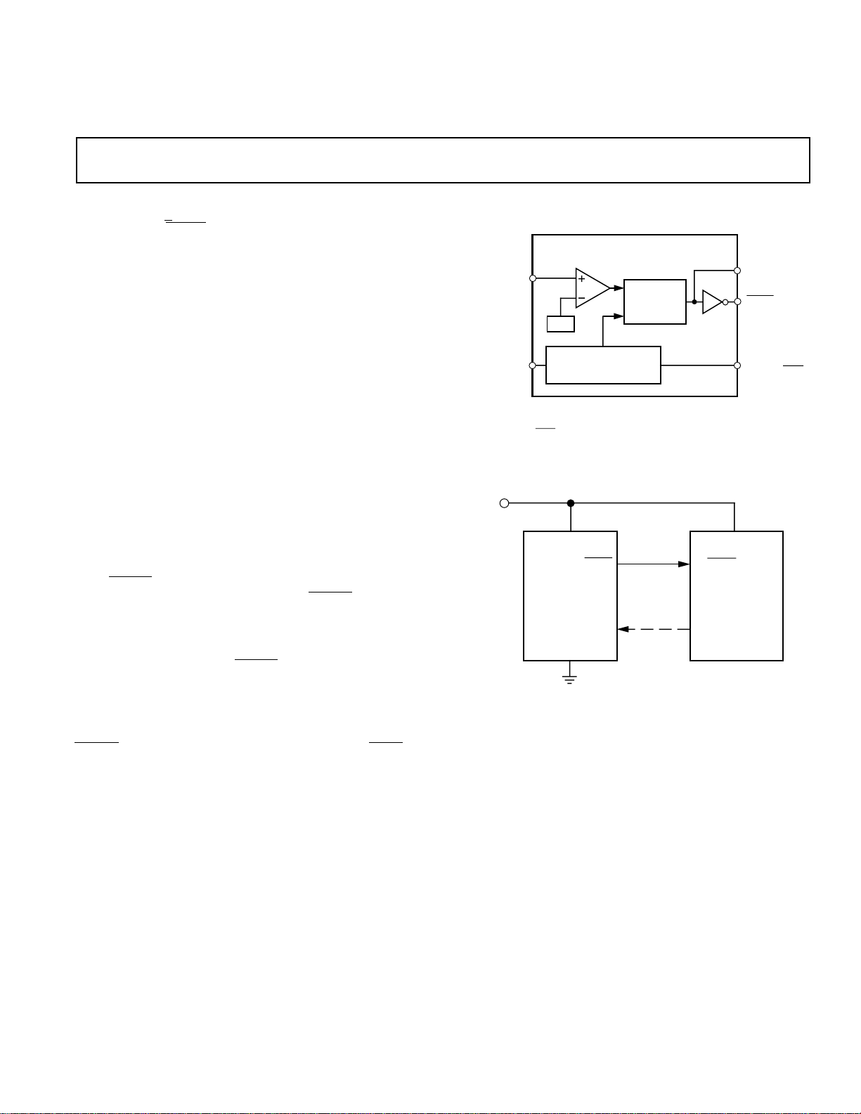
GENERAL DESCRIPTION
The ADM698/ADM699 supervisory circuits provide power
supply monitoring and watchdog timing for microprocessor
systems.
The ADM698 monitors the 5 V V
ates a
RESET pulse during power up, power down and during
low voltage “Brown Out” conditions. The
guaranteed to be functional (logic low) with V
The ADM699 features an identical monitoring circuit as in the
ADM698 plus an additional watchdog timer input to monitor
microprocessor activity. The
watchdog input is not toggled within the 1 second watchdog
timeout period.
Both parts are available in 8-pin plastic DIP and 16-lead SOIC
packages. The 16-lead SOIC contains additional outputs
RESET (without inversion) and Watchdog Output WDO
(ADM699 only).
grade for MAX698/MAX699
RESET Assertion with VCC = 1 V
power supply and gener-
CC
RESET output is
as low as 1 V.
CC
RESET output is forced low if the
Supervisory Circuits
ADM698/ADM699
FUNCTIONAL BLOCK DIAGRAM
TYPICAL APPLICATION CIRCUIT
REV. 0
Information furnished by Analog Devices is believed to be accurate and
reliable. However, no responsibility is assumed by Analog Devices for its
use, nor for any infringements of patents or other rights of third parties
which may result from its use. No license is granted by implication or
otherwise under any patent or patent rights of Analog Devices.
One Technology Way, P.O. Box 9106, Norwood, MA 02062-9106, U.S.A.
Tel: 617/329-4700 Fax: 617/326-8703
Page 2
ADM698/ADM699–SPECIFICATIONS
WARNING!
ESD SENSITIVE DEVICE
(VCC = +5 V 6 10%, TA = T
MIN
to T
unless otherwise noted)
MAX
Parameter Min Typ Max Units Test Conditions/Comments
VCC Operating Voltage Range 3.0 5.5 V
Supply Current 0.6 1.95 mA
Power-Down Reset Assertion 4.5 4.65 4.73 V
Power-Up Reset Deassertion 4.73 V
Reset Threshold Hysteresis 40 mV
Reset Active Time 140 200 280 ms T
Watchdog Timeout Period (ADM699) 1.0 1.6 2.25 s T
= +25°C, V
A
= +25°C, V
A
= +5 V
CC
= +5 V
CC
Minimum WDI Input Pulse Width 50 ns VIL = 0.4, VIH = 3.5 V
RESET Output Voltage 0.4 V I
RESET Output Voltage (VCC = 1 V) 4 200 mV I
3.5 V I
RESET and
WDO Output Voltage 0.4 V I
3.5 V I
= 1.6 mA, Vcc = 4.4 V
SINK
= 10 µA, V
SINK
= 1 µA, V
SOURCE
= 1.6 mA, VCC = 5 V
SINK
= 1 µA, V
SOURCE
= 1.0 V
CC
CC
CC
= 5 V
= 4.4 V
RESET Output Short Circuit Current 25 mA Output Sink Current
WDI Input Threshold (ADM699)
Logic Low 0.8 V
Logic High 3.5 V
WDI Input Current 20 50 µA WDI = V
CC
, T
A
= +25°C
–50 –20 µA WDI = 0 V, TA = +25°C
Specifications subject to change without notice.
ABSOLUTE MAXIMUM RATINGS*
(TA = +25°C unless otherwise noted)
VCC . . . . . . . . . . . . . . . . . . . . . . . . . . . . . . . . . . –0.3 V to +6 V
All Other Inputs . . . . . . . . . . . . . . . . . . . –0.3 V to V
+ 0.3 V
CC
Power Dissipation 8-Pin DIP . . . . . . . . . . . . . . . . . . . . 500 mW
θ
, Thermal Impedance . . . . . . . . . . . . . . . . . . . . +120°C/W
JA
Power Dissipation 16-Pin SOIC . . . . . . . . . . . . . . . . . 375 mW
θ
, Thermal Impedance . . . . . . . . . . . . . . . . . . . . +110°C/W
JA
Model Range Option
ADM698AN –40°C to +85°C N-8
ADM698AR –40°C to +85°C R-16
ADM698AQ –40°C to +85°C Q-8
ADM698SQ –55°C to +125°C Q-8
ORDERING GUIDE
Temperature Package
Power Dissipation 8-Pin Cerdip . . . . . . . . . . . . . . . . . . 500 mW
θ
, Thermal Impedance . . . . . . . . . . . . . . . . . . . . +125°C/W
JA
Operating Temperature Range
Industrial (A Version) . . . . . . . . . . . . . . . . . –40°C to +85°C
Extended (S Version) . . . . . . . . . . . . . . . . .–55°C to +125°C
ADM699AN –40°C to +85°C N-8
ADM699AR –40°C to +85°C R-16
ADM699AQ –40°C to +85°C Q-8
ADM699SQ –55°C to +125°C Q-8
Storage Temperature Range . . . . . . . . . . . . . –65°C to +150°C
Lead Temperature (Soldering, 10 secs) . . . . . . . . . . . . +300°C
Vapor Phase (60 secs) . . . . . . . . . . . . . . . . . . . . . . . +215°C
Infrared (15 secs) . . . . . . . . . . . . . . . . . . . . . . . . . . . +220°C
*Stresses above those listed under “Absolute Maximum Ratings may cause perma-
nent damage to the device. This is a stress rating only and functional operation of
the device at these or any other conditions above those listed in the operational
sections of this specification is not implied. Exposure to absolute maximum ratings
for extended periods of time may affect device reliability.
CAUTION
ESD (electrostatic discharge) sensitive device. Electrostatic charges as high as 4000 V readily
accumulate on the human body and test equipment and can discharge without detection.
Although the ADM698/ADM699 features proprietary ESD protection circuitry, permanent
damage may occur on devices subjected to high energy electrostatic discharges. Therefore, proper
ESD precautions are recommended to avoid performance degradation or loss of functionality.
–2–
REV. 0
Page 3

PIN FUNCTION DESCRIPTION
ADM698/ADM699
PIN CONFIGURATION (DIP)
Mnemonic Function
V
CC
+5 V Power Supply Input.
GND 0 V. Ground reference for all signals.
RESET Logic Output. RESET goes low whenever V
CC
falls below the reset voltage threshold (4.65 V
typ).
RESET remains low for a minimum of
140 ms after V
returns to 5 V. RESET also
CC
goes low for a minimum of 140 ms if the watchdog
timer is enabled but not serviced within its time-
out period.
WDI Watchdog Input. WDI is a three level input. If
WDI remains either high or low for longer than
the watchdog timeout period,
and
WDO goes low. The timer resets with each
RESET pulses low
transition on the WDI line. The watchdog timer
may be disabled if WDI is left floating or is driven
to midsupply.
RESET (SOIC packages only) Logic Output. RESET is
an active high output. It is the inverse of
RESET.
WDO (SOIC ADM699 only) Logic Output. The
Watchdog Output,
WDO, goes low if WDI
remains either high or low for longer than the
watchdog timeout period.
WDO is set high by the
next transition at WDI. If WDI is unconnected or
at midsupply, the watchdog timer is disabled and
WDO remains high.
V
V
GND
GND
1
CC
2
CC
3
4
ADM698/
ADM699
O
TOP VIEW
TOP VIEW
(Not to Scale)
(Not to Scale)
*
( ) ADM699 ONLY
8
7
6
5
GND
RESET
NC (WDI)
NC
*
PIN CONFIGURATION (SOIC)
GND
1
V
V
GND
NC
NC
NC
NC
CC
CC
O
2
ADM698/
TOP VIEW
3
ADM699
(Not to Scale)
4
TOP VIEW
5
(Not to Scale)
6
710
89
*( ) ADM699 ONLY
RESET
16
RESET
15
NC (WDO)*
14
NC
13
NC
12
NC (WDI)
11
NC
GND
*
TYPICAL PERFORMANCE CURVES
A4
3.36 V
100
90
10
0%
1V
1V
Figure 1. RESET Output Voltage vs. V
500ms
4.70
VCC = +5V
4.68
4.66
4.64
RESET VOLTAGE THRESHOLD – V
4.62
20 40 60 80 100 120
Figure 3. RESET Voltage Threshold vs. Temperature
CC
POWER UP
POWER DOWN
TEMPERATURE –
215
210
205
200
RESET ACTIVE TIME – ms
195
20
40 60 80 100 120
TEMPERATURE –
VCC = +5V
°
C
Figure 2. RESET Active Time vs. Temperature
°
C
REV. 0
–3–
Page 4

ADM698/ADM699
0.019 (0.49)
0.05 (1.27)
REF
0.104
(2.65)
0.012
(0.3)
0.413 (10.50)
0.419
(10.65)
0.299
(7.60)
1
8
9
16
0.042
(1.07)
0.013
(0.32)
0.030
(0.75)
CIRCUIT INFORMATION
Power Fail RESET
A precision voltage detector monitors VCC and generates a
RESET output to hold the microprocessor’s Reset line low when
V
falls below the reset threshold (4.65 V) (see Figure 4). The
CC
reset voltage threshold is set to accommodate a 5% variation on
V
. The voltage detector has 40 mV hysteresis to ensure that
CC
glitches on V
On power up, an internal monostable holds
140 ms after V
do not activate the RESET output.
CC
RESET low for
rises above the reset threshold. This allows the
CC
power supply to stabilize on power up and also prevents repeated toggling of
RESET even if the 5 V power drops out and
recovers with each power line cycle. In order to prevent
mistriggering due to transient voltage spikes, it is recommended
that a 0.1 µF capacitor be connected at the V
RESET output is guaranteed to remain low with VCC as
The
CC
pin.
low as 1 V. This holds the microprocessor in a stable shutdown
condition as the power supply comes up.
On the 16-lead SOIC package, an active high RESET output is
also provided. This is the complement of
RESET and is in-
tended for microprocessors requiring an active high signal.
V
CC
V
2
V
1
V
2
V
1
Watchdog Timer (ADM699 Only)
The watchdog timer input (WDI) monitors an I/O line from the
µP system. The µP must toggle this input once every 1.6 sec-
onds to verify correct software execution. Failure to toggle the
line indicates that the µP system is not correctly executing its
program and may be tied up in an endless loop. If this happens,
a reset pulse is generated to initialize the processor.
The WDI input is a three level input and will recognize a low
to- high or a high-to-low transition on its input. The watchdog
timer is reset by each WDI transition and then begins its
timeout period. If the WDI pin remains either high or low, reset
pulses will be issued every 1.6 seconds typically. If the watchdog timer is not needed, the WDI input should be left floating.
The Watchdog Output (
WDO) (SOIC package Only) provides
watchdog status information. It is driven low if WDI is not
toggled within the watchdog timeout period. It goes high at the
next WDI transition. It is also set high when V
falls below the
CC
reset threshold.
WDI
WDO
C1784–18–4/93
RESET
t
1
V1 = RESET VOLTAGE THRESHOLD
V2 = RESET VOLTAGE THRESHOLD +
THRESHOLD HYSTERESIS
t
= RESET TIME
1
t
1
Figure 4. Watchdog Timeout Period vs. Temperature
Dimensions shown in inches and (mm).
8-Pin Plastic DIP
(N-8)
RESET
Figure 5. Watchdog Timeout Period and Reset Active Time
OUTLINE DIMENSIONS
8-Pin Cerdip
(Q-8)
MAX
BSC
0.320 (8.13)
0.290 (7.37)
5
4
0.310 (7.87)
0.220 (5.59)
0.060 (1.52)
0.015 (0.38)
0.150
(3.81)
MIN
0.070 (1.78)
0.30 (0.76)
PIN 1
0.200
(5.08)
MAX
SEATING
PLANE
0.022 (0.558)
0.014 (0.356)
8
1
0.420 (10.67)
0.100 (2.54)
t
2
t
1
t
= RESET TIME
1
t
= WATCHDOG TIME OUT PERIOD
2
t
1
16-Lead SOIC
t
2
(R-16)
t
1
PRINTED IN U.S.A.
0.015 (0.381)
0.008 (0.204)
–4–
REV. 0
 Loading...