

Page 1

ADM6926
26 port 10/100 Mbps Ethernet Switch
Controller
Version 1.0
ADMtek.com.tw
Information in this document is provided in connection with ADMtek products. ADMtek may make
changes to specifications and product descriptions at any time, without notice. Designers must not rely on
the absence or characteristics of any features or instructions marked “reserved” or “undefined”. ADMtek
reserves these for future definition and shall have no responsibility whatsoever for conflicts or
incompatibilities arising from future changes to them
The products may contain design defects or errors know as errata, which may cause the product to deviate
from published specifications. Current characterized errata are available on request. To obtain latest
documentation please contact you local ADMtek sales office or visit ADMtek’s website at
http://www.ADMtek.com.tw
*Third-party brands and names are the property of their respective owners.
Page 2

ADMtek Inc. V1.0
About this Manual
General Release
Intended Audience
ADMtek’s Customers
Structure
This Data sheet contains 5 chapters
Chapter 1 Product Overview
Chapter 2 Interface Description
Chapter 3 Function Description
Chapter 4. Electrical Specification
Chapter 5. Packaging
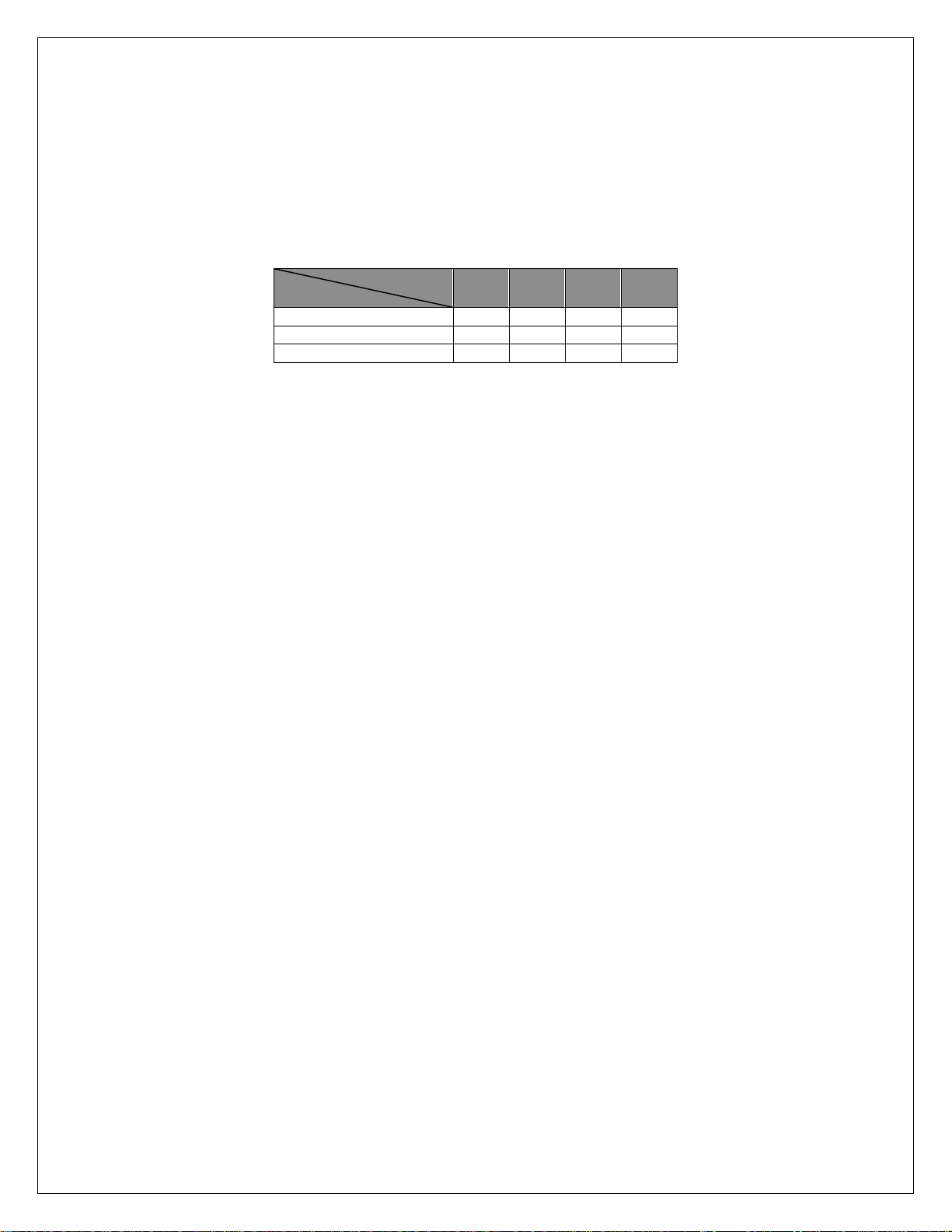
Revision History
Date Version Change
08 Aug 2003
1.0 1. First release of ADM6926
Customer Support
ADMtek Incorporated,
2F, No.2, Li-Hsin Rd.,
Science-based Industrial Park,
Hsinchu, 300, Taiwan, R.O.C.
Sales Information
Tel + 886-3-5788879
Fax + 886-3-5788871
Page 3

ADMtek Inc. V1.0
Table of Contents
Chapter 1 Product Overview........................................................................................1-1
1.1 Overview.......................................................................................................... 1-1
1.2 Features............................................................................................................ 1-1
1.3 Block Diagram................................................................................................. 1-2
1.4 Abbreviations................................................................................................... 1-3
1.5 Conventions ..................................................................................................... 1-4
1.5.1 Data Lengths............................................................................................1-4
1.5.2 Register Type Descriptions......................................................................1-4
1.5.3 Pin Type Descriptions..............................................................................1-4
Chapter 2 Interface Description...................................................................................2-1
2.1 Pin Diagram – ADM6926 (SS-SMII Interface)..................................................... 2-1
2.2 Pin Description................................................................................................. 2-2
2.2.1 SS-SMII Networking Interface, 60 pins ...................................................2-2
2.2.2 MII/RMII Interface, 28pins......................................................................2-3
2.2.3 Power/Ground..........................................................................................2-5
2.2.4 Miscellaneous pins, 16 pins.....................................................................2-5
Chapter 3 Function Description...................................................................................3-1
3.1.1 Basic Operation.......................................................................................3-1
3.1.2 Address Learning.....................................................................................3-1
3.1.3 Address Aging..........................................................................................3-2
3.1.4 Address Recognition and Packet Forwarding.........................................3-3
3.1.5 Trunking Port Forwarding ......................................................................3-4
3.1.6 Illegal Frames..........................................................................................3-4
3.1.7 Back off Algorithm...................................................................................3-4
3.1.8 Buffers and Queues..................................................................................3-4
3.1.9 Half Duplex Flow Control.......................................................................3-5
3.1.10 Full Duplex Flow Control........................................................................3-5
3.1.11 Inter-Packet Gap (IPG) ...........................................................................3-5
3.1.13 Priority Control .......................................................................................3-6
3.1.14 Alert LED Display....................................................................................3-7
3.1.15 Broadcast Storm Filter ............................................................................3-7
3.1.16 Collision LED Display.............................................................................3-7
3.1.17 Bandwidth Control...................................................................................3-8
3.1.18 Smart Discard..........................................................................................3-8
3.1.19 Security Support.......................................................................................3-8
3.1.20 Smart Counter Support............................................................................3-8
3.1.21 Length 1536 Mode ...................................................................................3-8
3.1.22 PHY Management (MDC/MDIO Interface).............................................3-8
3.1.23 Forward Special Packets to the CPU Port..............................................3-9
3.1.24 Special TAG...........................................................................................3-10
3.1.25 Port 24 and Port 25 Interface (Only SS-SMII package support)...........3-12
3.1.26 Hardware, EEPROM and SMI Interface for Configuration..................3-13
3.2 EEPROM Register Format ............................................................................3-17
3.2.1 Signature (Index: 0h).............................................................................3-20
3.2.2 Global Configuration Register (Index: 1h)............................................3-20
ADM6926 i
Page 4

ADMtek Inc. V1.0
3.2.3 Port Configuration Registers (Index: 2h ~ 1bh)....................................3-21
3.2.4 Miscellaneous Configuration (Index: 1ch)............................................3-23
3.2.5 VLAN(TOS) Priority Map (Index: 1dh).................................................3-23
3.2.6 Forwarding Group Outbound Port Map Low .......................................3-24
3.2.7 Forwarding Group Outbound Port Map High ......................................3-25
3.2.8 P0 VID and PVID Shift (Index: 5eh) .....................................................3-25
3.2.9 P1~P25 VID Configuration...................................................................3-26
3.2.10 P0, P1, P2, P3 Bandwidth Control Register (Index: 78h).....................3-26
3.2.11 P4, P5, P6, P7 Bandwidth Control Register (Index: 79h).....................3-27
3.2.12 P8, P9, P10, P11 Bandwidth Control Register (Index: 7ah).................3-27
3.2.13 P12, P13, P14, P15 Bandwidth Control Register (Index: 7bh).............3-28
3.2.14 P16, P17, P18, P19 Bandwidth Control Register (Index: 7ch).............3-28
3.2.15 P20, P21, P22, P23 Bandwidth Control Register (Index: 7dh).............3-29
3.2.16 P24, P25 Bandwidth Control Register (Index: 7eh)..............................3-29
3.2.17 Bandwidth Control Enable Register Low (Index: 7fh)..........................3-30
3.2.18 Bandwidth Control Enable Register High (Index: 80h)........................3-30
3.2.19 Reserved Registers (Index: 81h~8ah)....................................................3-30
3.2.20 Customized PHY Control Group 0 (Index: 8bh)....................................3-31
3.2.21 Customized PHY Control Group 1 (Index: 8ch)....................................3-31
3.2.22 Customized PHY Control Group 2 (Index: 8dh)....................................3-32
3.2.23 Customized PHY Control Group 3 (Index: 8eh)....................................3-32
3.2.24 Group 0 PHY Customized DATA 0 (Index: 8fh)....................................3-32
3.2.25 Group 0 PHY Customized DATA 1 (Index: 90h)...................................3-32
3.2.26 Group 1 PHY Customized DATA 0 (Index: 91h)...................................3-33
3.2.27 Group 1 PHY Customized DATA 1 (Index: 92h)...................................3-33
3.2.28 Group 2 PHY Customized DATA 0 (Index: 93h)...................................3-33
3.2.29 Group 2 PHY Customized DATA 1 (Index: 94h)...................................3-33
3.2.30 Group 3 PHY Customized DATA 0 (Index: 95h)...................................3-33
3.2.31 Group 3 PHY Customized DATA 1 (Index: 96h)...................................3-33
3.2.32 PHY Customized Enable Register (Index: 97h).....................................3-33
3.2.33 PPPOE Control Register0 (Index: 98h)................................................3-34
3.2.34 PPPOE Control Register 1 (Index: 99h)...............................................3-34
3.2.35 PHY Control Register 0 (Index: 9ah) ....................................................3-35
3.2.36 PHY Control Register 1 (Index: 9bh) ....................................................3-35
3.2.37 Disable MDIO Active Register 0 (Index: 9ch).......................................3-36
3.2.38 Disable MDIO Active Register 1 (Index: 9dh) ......................................3-36
3.2.39 Port Disable Register 0 (Index: 9eh).....................................................3-37
3.2.40 Port Disable Register 1 (Index: 9fh)......................................................3-37
3.2.41 IGMP Snooping Control Register 0 (Index: a0h)..................................3-37
3.2.42 IGMP Snooping Control Register 1 (Index: a1h)..................................3-38
3.2.43 CPU Control Register (Index: a2h).......................................................3-38
3.2.44 Special MAC Forward Control Register 0 (Index: a3h) .......................3-39
3.2.45 Special MAC Forward Control Register 2 (Index: a4h) .......................3-40
3.2.46 Special MAC Forward Control Register 2 (Index: a5h) .......................3-40
3.2.47 Trunking Enable Register 0 (Index: a6h) ..............................................3-41
3.2.48 Trunking Enable Register 1 (Index: a7h) ..............................................3-41
ADM6926 ii
Page 5

ADMtek Inc. V1.0
3.3 Switch Register Map...................................................................................... 3-42
3.3.1 Version ID (Offset: 0h) ..........................................................................3-42
3.3.2 Link Status (Offset: 1h)..........................................................................3-42
3.3.3 Speed Status (Offset: 2h)........................................................................3-43
3.3.4 Duplex Status (Offset: 3h)......................................................................3-44
3.3.5 Flow Control Status (Offset: 4h)............................................................3-44
3.3.6 Address Table Control and Status Register...........................................3-45
3.3.7 PHY Control Register (Offset: bh).........................................................3-51
3.3.8 Hardware Status (Offset: dh).................................................................3-51
3.3.9 Receive Packet Count Overflow (Offset: eh).........................................3-52
3.3.10 Receive Packet Length Count Overflow (Offset: fh)..............................3-53
3.3.11 Transmit Packet Count Overflow (Offset: 10h).....................................3-53
3.3.12 Transmit Packet Length Count Overflow (Offset: 11h).........................3-54
3.3.13 Error Count Overflow (Offset: 12h)......................................................3-54
3.3.14 Collision Count Overflow (Offset: 13h).................................................3-55
3.3.15 Renew Counter Register (Offset: 14h)...................................................3-56
3.3.16 Read Counter Control & Status Register ..............................................3-57
3.3.17 Reload MDIO Register (Offset: 17h).....................................................3-57
3.3.18 Spanning Tree Port State 0 (Offset: 18h) ..............................................3-58
3.3.19 Spanning Tree Port State 1 (Offset: 19h) ..............................................3-58
3.3.20 Source Port Register (Offset: 1ah) ........................................................3-59
3.3.21 Transmit Port Register (Offset: 1bh).....................................................3-59
3.3.22 Counter Register: Offset Hex. 0100h ~ 019b.........................................3-59
Chapter 4 Electrical Specification................................................................................4-1
4.1 DC Characterization......................................................................................... 4-1
4.1.1 Absolute Maximum Rating.......................................................................4-1
4.1.2 Recommended Operating Conditions......................................................4-1
4.1.3 DC Electrical Characteristics for 3.3V Operation..................................4-1
4.2 AC Characterization......................................................................................... 4-2
4.2.1 XI/OSCI (Crystal/Oscillator) Timing.......................................................4-2
4.2.1 Power On Reset........................................................................................4-2
4.2.2 EEPROM Interface Timing......................................................................4-3
4.2.3 10Base-TX MII Output Timing ................................................................4-3
4.2.4 10Base-TX MII Input Timing...................................................................4-4
4.2.5 100Base-TX MII Output Timing ..............................................................4-5
4.2.6 100Base-TX MII Input Timing.................................................................4-5
4.2.7 Reduced MII Timing ................................................................................4-6
4.2.8 SS_SMII Transmit Timing........................................................................4-7
4.2.9 SS_SMII Receive Timing..........................................................................4-7
4.2.10 Serial Management Interface (MDC/MDIO) Timing..............................4-8
Chapter 5 Packaging......................................................................................................5-1
ADM6926 iii
Page 6

ADMtek Inc. V1.0
List of Figures
Figure 1-1 ADM6926 Block Diagram............................................................................. 1-2
Figure 2-1 ADM6926 Pin Diagram ................................................................................. 2-1
Figure 3-1 The Search Pointer .......................................................................................3-48
Figure 3-2 Address Table Mapping to Output Port MAP.............................................. 3-50
Figure 4-1 Crystal/Oscillator Timing...............................................................................4-2
Figure 4-2 Power on reset timing.....................................................................................4-2
Figure 4-3 EEPROM Interface Timing............................................................................4-3
Figure 4-4 10Base-TX MII Output Timing ..................................................................... 4-3
Figure 4-5 10Base-TX MII Input Timing........................................................................ 4-4
Figure 4-6 100Base-TX MII Output Timing ................................................................... 4-5
Figure 4-7 100Base-TX MII Input Timing...................................................................... 4-5
Figure 4-8 Reduced MII Timing (1 of 2)......................................................................... 4-6
Figure 4-9 Reduced MII Timing (2 of 2)......................................................................... 4-6
Figure 4-10 SS_SMII Transmit Timing........................................................................... 4-7
Figure 4-11 SS_SMII Receive Timing ............................................................................ 4-7
Figure 4-12 Serial Management Interface (MDC/MDIO) Timing.................................. 4-8
List of Table
Table 4-4-1 Electrical Absolute Maximum Rating.......................................................... 4-1
Table 4-4-2 Recommended Operating Conditions .......................................................... 4-1
Table 4-4-3 DC Electrical Characteristics for 3.3V Operation........................................ 4-1
Table 4-4 Crystal/Oscillator Timing................................................................................ 4-2
Table 4-5 Power on reset timing...................................................................................... 4-3
Table 4-6 EEPROM Interface Timing............................................................................. 4-3
Table 4-7 10Base-TX MII Output Timing....................................................................... 4-4
Table 4-8 10Base-TX MII Input Timing ......................................................................... 4-4
Table 4-9 100Base-TX MII Output Timing..................................................................... 4-5
Table 4-10 100Base-TX MII Input Timing ..................................................................... 4-6
Table 4-11 Reduced MII Timing ..................................................................................... 4-6
Table 4-12 SS_SMII Transmit Timing............................................................................ 4-7
Table 4-13 SS_SMII Receive Timing.............................................................................. 4-8
Table 4-14 Serial Management Interface (MDC/MDIO) Timing ................................... 4-8
ADM6926 iv
Page 7

ADM6926 Product Review
Chapter 1 Product Overview
1.1 Overview
The ADM6926 is a high performance/low cost, twenty six-port 10/100 Mbps Ethernet
Switch Controller with all ports supporting 10/100 Mbps full duplex switch function.
The ADM6926 is intended for applications to standalone-bridge for the low cost etherswitch market. ADM6926 can be programmed trunking port active. The trunking port
can be connected to server or stacking two switch boxes to enhance the performance.
The ADM6926 also supports back-pressure in half duplex mode and 802.3x flow control
in full duplex mode. When back-pressure is enabled, and there is no receive buffer
available for the incoming packet, the ADM6926 will force a JAM pattern on the
receiving port in half duplex mode and transmit the 802.3x packet back to receiving end
in full duplex mode.
An intelligent address recognition algorithm makes ADM6926 to recognize up to 4096
different MAC addresses and enables filtering and forwarding at full wire speed.
The ADM6926 has embedded SRAM for the proprietary buffer management. The SRAM
is used to store the incoming/outgoing packets. These buffers provide elastic storage for
transferring data between low-speed and high-speed segments and buffers are efficiently
allocated to improve the efficiency.
1.2 Features
• Support twenty four 10/100M auto-detect Half/Full duplex switch ports with SS-SMII
interface and two 10/100M Half/Full duplex port with RMII/MII interface
• Supports up to 4096 MAC addresses table (4-way hashing)
• Support two queue for QOS (1:2 or 1:4 or 1:8 or 1:16)
• Support Port-base, 802.1p and IP TOS priority
• Supports store & forward architecture and Performs forwarding and filtering at non-
blocking full wire speed
• Support buffer allocation with 256 bytes each
• Supports aging function and 802.3x flow control for full duplex and back-pressure
function for half duplex operation in case buffer is full
• Support packet length up to 1536 bytes
• Support Congestion Flow Control
• Broadcast storm filter and Alert LED
• Port-base VLAN and adjustable VLAN to support up to 32 VLAN group
• serial CPU interface for counter and port status output
• CPU can see-through to access PHY
• flexible port trunking on fault tolerance and load balance
• per port 32bits smart counter for Rx/Tx byte/packet count, error count and collision
count
ADMtek Inc. 1-1
Page 8
ADM6926 Product Review
• rate-limit control (64K/128K/256K/512K/1M/4M/10M/20M)
• per port auto learning enable/disable and if disable, forward non-learned packet to
CPU
• MAC address table accessible (in each entry, reserve one bit for CPU to
enable/disable aging out)
• forward special multicast, BPDU, GMRP, GVRP and IGMP packets to CPU port
• 128 pin QFP package with 3.3V/1.8V power supply
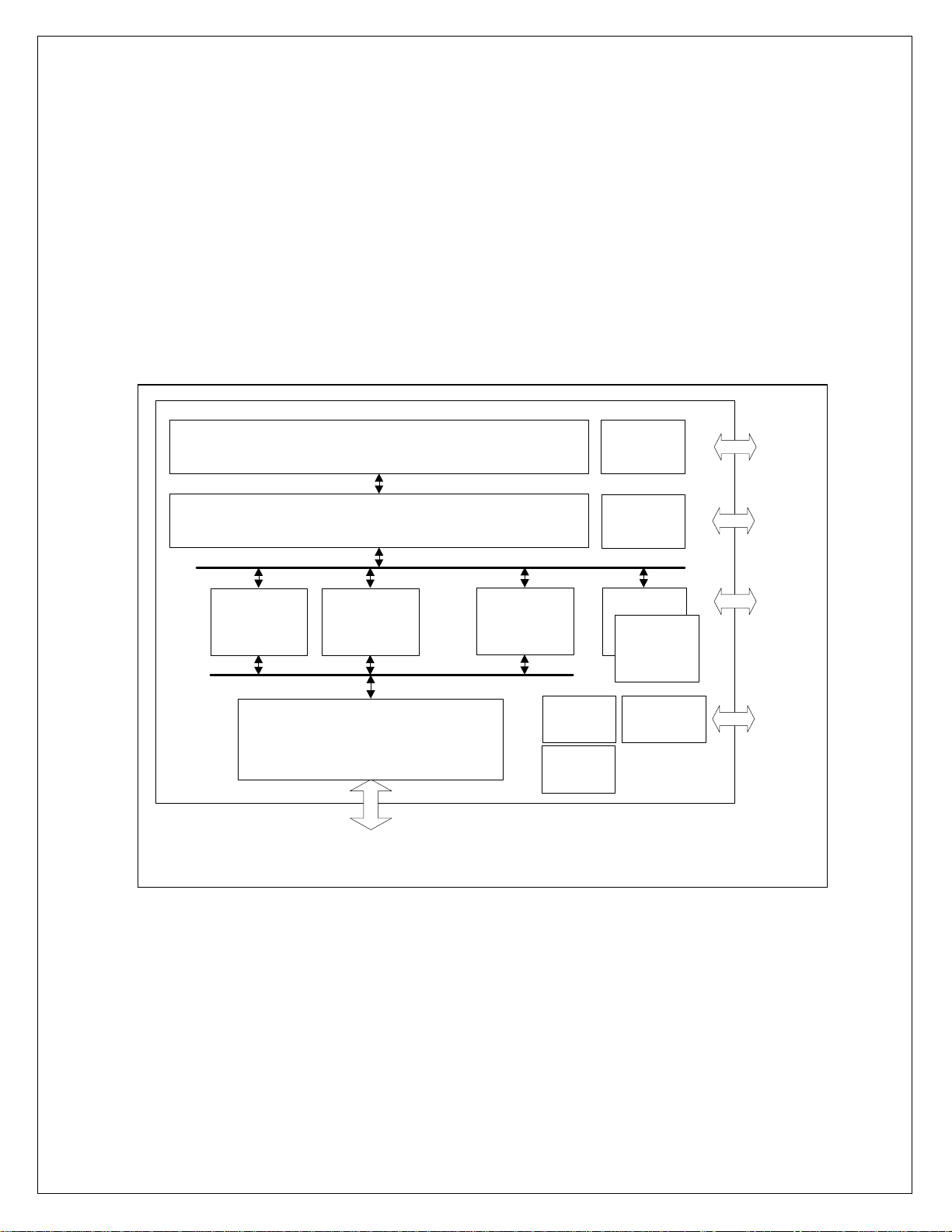
1.3 Block Diagram
10/100M
MAC
Embedded Memory
Switching Fa bric
10/100M
MAC
Interface Convertor
SS- SM I I
Interface
...
10/100M
MAC
CLOCK
GENERATOR
BIAS
Memory
BIST
EEPROM
Control
10/100M
10/100M
MAC
MAC
PHY Control
Cl ock /
LED
Interface
93C66
Interface
MII/RMII
Interface
MDC/
MDIO
Figure 1-1 ADM6926 Block Diagram
ADMtek Inc. 1-2
Page 9

ADM6926 Product Review
1.4 Abbreviations
BPDU Bridge Protocol Data Unit
CRC Cyclic Redundancy Check
CRSDV Carrier Sense and Data Valid
DA Destination Address
DUPCOL Duplex and Collision
EDI EEPROM Data Input
EDO EEPROM Data Output
EECS EEPROM Chip Select
EESK EEPROM Serial Clock
ESD End of Stream Delimiter
FCS Frame Check Sequence
FET Field Effect Transistor
GARP Generic Attribute Registration Protocol
GMRP GARP Multicast Registration Protocol
GVRP GARP VLAN Registration Protocol
IGMP Internet Group Management Protocol
IPG Inter-Packet Gap
MAC Media Access Controller
MDC Management Data Clock
MDIO Management Data Input/Output
MII Media Independent Interface
PHY Physical Layer
PLL Phase Lock Loop
PPPoE Point to Point Protocol over Ethernet
PVID Port VLAN ID
QFP Quad Flat Pack
QOS Quality of Service
RMII Reduced Media Independent Interface
SA Source Address
SS-SMII Source Synchronous Serial MII
TA Turn Around
TOS Type of Service
TTL Transistor Transistor Logic
UNIQUE Universal Queue management
VID VLAN ID
VIH Voltage Input High
VIL Voltage Input Low
VLAN Virtual LAN
ADMtek Inc. 1-3
Page 10

ADM6926 Product Review
1.5 Conventions
1.5.1 Data Lengths
qword 64-bits
dword 32-bits
word 16-bits
byte 8 bits
nibble 4 bits
1.5.2 Register Type Descriptions
Register Type Description
RO Read Only
R/W Read and Write capable
SC Self-clearing
LL Latching low, unlatch on read
LH Latching high, unlatch on read
COR Clear On Read
1.5.3 Pin Type Descriptions
Pin Type Description
I: Input
O: Output
I/O: Bi-directional
OD: Open drain
SCHE: Schmitt Trigger
PU: Pull Up
PD: Pull Down
ADMtek Inc. 1-4
Page 11
ADM6926 Interface Description
Chapter 2 Interface Description
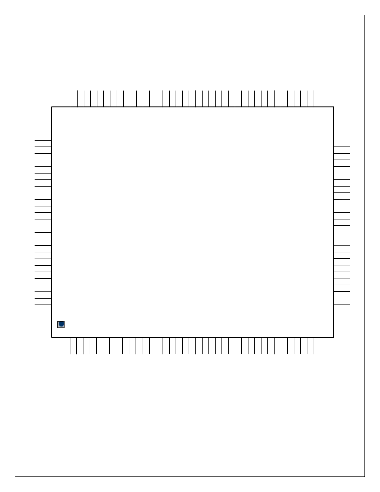
2.1 Pin Diagram – ADM6926 (SS-SMII Interface)
102
101
100
999897969594939291
M1TXCLK
M1RXCLK
M1RXDV
M1RXD[0]
M1RXD[1]
M1RXD[2]
M1RXD[3]
EESK
EDI
EDO
908988878685848382818079787776
M0RXD[1]
M0RXD[2]
M0RXD[3]
M1CRS
M1COL
M1TXD[3]
M1TXD[2]
M1TXD[1]
M1TXD[0]
VCCIK
GNDIK
M1TXEN
M0RXD[0]
VCC3O
GNDO
75
M0TXD[0]
M0TXEN
M0TXCLK
M0RXCLK
M0RXDV
M0TXD[2]
M0TXD[1]
7069686766
GNDIK
M0CRS
M0COL
M0TXD[3]
65
SRXD2[7]
VCCIK
71
72
73
74
103
104
105
106
107
108
109
110
111
112
113
114
115
116
117
118
119
120
121
122
123
124
125
126
127
128
ALERT
STXD0[0]
EECS
SRXD0[0]
STXD0[1]
SRXD0[1]
STXD0[2]
VCC3O
GNDO
SRXD0[2]
SYNC_TX0
STXD0[3]
SYNC_RX0
SRXD0[3]
CLK_TX0
STXD0[4]
CLK_RX0
SRXD0[4]
VCCIK
GNDIK
STXD0[5]
SRXD0[5]
STXD0[6]
SRXD0[6]
STXD0[7]
VCC3O
ADM6926
STXD2[7]
SRXD2[6]
STXD2[6]
SRXD2[5]
STXD2[5]
RESETL
SRXD2[4]
CLK_RX2
STXD2[4]
CLK_TX2
SRXD2[3]
SYNC_RX2
GNDO
VCC3O
GNDIK
VCCIK
STXD2[3]
SYNC_TX2
SRXD2[2]
STXD2[2]
SRXD2[1]
STXD2[1]
SRXD2[0]
STXD2[0]
SRXD1[7]
STXD1[7]
64
63
62
61
60
59
58
57
56
5
5
54
53
52
51
50
49
48
47
46
45
44
43
42
41
40
39
GNDO
SRXD0[7]
STXD1[0]
SRXD1[0]
CKO50M
STXD1[1]
CKO25M
SRXD1[1]
STXD1[2]
SRXD1[2]
VCCRG
GNDRG
VREF
CONTROL
VCCPLL
GNDPLL
SYNC_TX1
STXD1[3]
MDC
MDIO
TEST2XIXO
2
1
6453789
15
10
11
141316
12
171819
21
20
TEST1
SYNC_RX1
SRXD1[3]
CLK_TX1
VCC3O
GNDO
STXD1[4]
CLK_RX1
SRXD1[4]
STXD1[5]
VCCIK
GNDIK
SRXD1[5]
STXD1[6]
SRXD1[6]
34
33
32
24
23
22
2526272829
31
30
353637
38
Figure 2-1 ADM6926 Pin Diagram
ADMtek Inc. 2-1
Page 12

ADM6926 Interface Description
2.2 Pin Description
ADM6926 pins are categorized into one of the following groups:
• Section 2.2.1 SS-SMII Networking Interface, 60 pins
• Section 2.2.2 MII/RMII Interface, 28pins
• Section 2.2.3 Power/Ground
• Section 2.2.4 Miscellaneous pins, 16 pins
2.2.1 SS-SMII Networking Interface, 60 pins
Name Type Pin # Description
SRXD0[0:7] I,
TTL
106,108,
112,116,
Port 0 to Port 7 SS-SMII Receive Data bit. The receive data
should be synchronous to the rising edge of CLK_RX0.
120,124,
126,2
SYNC_RX0 I,
TTL
115 Port 0 to Port 7 SS-SMII Synchronous signal. This signal is
synchronous to the rising edge of CLK_RX0. Active high
indicates the byte boundary.
CLK_RX0 I,
TTL
STXD0[0:7] O, TTL
8mA
119 Reference Receive Clock for Port 0 to Port 7. This signal is
125MHz input for SS-SMII interface.
104,107,
109,114,
Port 0 to Port 7 SS-SMII Transmit Data bit. The transmit
data is synchronous to the rising edge of CLK_TX0.
118,123,
125,127
SYNC_TX0 O, TTL
8mA
113 Port 0 to Port 7 SS-SMII Synchronous signal. This signal is
synchronous to the rising edge of CLK_TX0. Active high
indicates the byte boundary.
CLK_TX0 O, TTL
16mA
SRXD1[0:7] I,
TTL
117 Reference Transmit Clock for Port 0 to Port 7. This signal
is 125MHz output for SS-SMII interface.
4,8,10,26,
32,36,38,
Port 8 to Port 15 SS-SMII Receive Data bit. The receive
data should be synchronous to the rising edge of CLK_RX1.
40
SYNC_RX1 I,
TTL
25 Port 8 to Port 15 SS-SMII Synchronous signal. This signal
is synchronous to the rising edge of CLK_RX1. Active high
indicates the byte boundary.
CLK_RX1 I,
TTL
STXD1[0:7] O, TTL
8mA
31 Reference Receive Clock for Port 8 to Port 15. This signal
is 125MHz input for SS-SMII interface.
3,6,9,18,
30,33,37,
Port 8 to Port 15 SS-SMII Transmit Data bit. The transmit
data is synchronous to the rising edge of CLK_TX1.
39
SYNC_TX1 O, TTL
8mA
17 Port 8 to Port 15 SS-SMII Synchronous signal. This signal
is synchronous to the rising edge of CLK_TX1. Active high
indicates the byte boundary.
CLK_TX1 O, TTL 27 Reference Transmit Clock for Port 8 to Port 15. This
ADMtek Inc. 2-2
Page 13

ADM6926 Interface Description
Name Type Pin # Description
16mA signal is 125MHz output for SS-SMII interface.
SRXD2[0:7] I,
TTL
42,44,46,
54,58,61,
Port 16 to Port 23 SS-SMII Receive Data bit. The receive
data should be synchronous to the rising edge of CLK_RX2.
63,65
SYNC_RX2 I,
TTL
53 Port 16 to Port 23 SS-SMII Synchronous signal. This
signal is synchronous to the rising edge of CLK_RX2. Active
high indicates the byte boundary.
CLK_RX2 I,
TTL
STXD2[0:7] O, TTL
8mA
57 Reference Receive Clock for Port 16 to Port 23. This signal
is 125MHz input for SS-SMII interface.
41,43,45,
48,56,60,
Port 16 to Port 23 SS-SMII Transmit Data bit. The
transmit data is synchronous to the rising edge of CLK_TX2.
62,64
SYNC_TX2 O, TTL
8mA
47 Port 16 to Port 23 SS-SMII Synchronous signal. This
signal is synchronous to the rising edge of CLK_TX2. Active
high indicates the byte boundary.
CLK_TX2 O, TTL
16mA
55 Reference Transmit Clock for Port 16 to Port 23. This
signal is 125MHz output for SS-SMII interface.
2.2.2 MII/RMII Interface, 28pins
Name Type Pin # Description
M0CRS I,
TTL
68
MII Port0 Carrier Sense
This pin is internal pull_down.
PD
M0COL I,
TTL
69
MII Port0 Collision input
This pin is internal pull_down.
PD
M0TXD
[0:3]
I/O,
TTL
8mA
PD
73,72,71,
70
MII Port 0 Transmit Data Bit[0:3].
Synchronous to the rising edge of M0TXCLK.
RMII Port 0 Transmit Data Bit[0:1].
Synchronous to the rising edge of M0RXCLK.
RMIIMODE[1] : Value on M0TXD[3] will be latched at the
rising edge of RESETL to configure port 25 as RMII mode.
RMIIMODE[0] : Value on M0TXD[2] will be latched at the
rising edge of RESETL to configure port 24 as RMII mode.
M0TXEN I/O,
TTL
8mA
74
MII/RMII Port 0 Transmit Enable.
AGDIS. Value on this pin will be latched at the rising edge
of RESETL to set aging disable.
PD
M0TXCLK I,
TTL
75
MII Port 0 Transmit clock Input.
This pin is 25MHz input for MII interface.
PD
M0RXCLK I,
TTL
PD
76
MII/RMII Port 0 Receive Clock Input.
This pin is 25MHz input for MII interface and 50MHz
REFCLK input for RMII interface.
ADMtek Inc. 2-3
Page 14

ADM6926 Interface Description
Name Type Pin # Description
M0RXDV I,
TTL
PD
M0RXD
[0:3]
I,
TTL
PD
77
80,81,82,
83
MII Port 0 Receive Data Valid.
RMII Port 0 Carrier Sense/Receive Data Valid.
This pin is internal pull_down.
MII Port 0 Receive Data Bit[0:3].
RMII Port 0 Receive Data Bit[0:1].
If in RMII mode, M0RXD[3] used for ext_dup_enable and
M0RXD[2] used for ext_dup_full. Internal pull_down. See
Sec3.1.27 for details.
M1CRS I,
TTL
84
MII Port 1 Carrier Sense
This pin is internal pull_down.
PD
M1COL I,
TTL
85
MII Port 1 Collision input
This pin is internal pull_down.
PD
M1TXD
[0:3]
I/O,
TTL
8mA
89,88,87,
86
MII Port 1Transmit Data Bit[0:3].
Synchronous to the rising edge of M1TXCLK.
RMII Port 1Transmit Data Bit[0:1].
Synchronous to the rising edge of M1RXCLK.
BPEN. Value on M1TXD[3] will be latched at the rising
edge of RESETL to set Back_pressure enable. Internal
pull_up.
FCEN. Value on M1TXD[2] will be latched at the rising
edge of RESETL to set flow control enable. Internal pull_up.
TNKEN. Value on M1TXD[1] will be latched at the rising
edge of RESETL to set trunking enable. Internal pull_up.
IPGLVING. Value on M1TXD[0] will be latched at the
rising edge of RESETL to set shorter IPG. Internal
pull_down.
M1TXEN O, TTL
8mA
PU
M1TXCLK I,
TTL
92
MII Port 1 Transmit Enable.
ANEN. Value on this pin will be latched at the rising edge of
RESETL to set auto_negotiation enable. Internal pull_up.
93 MII Port1 Transmit clock Input. This signal is 25MHz
input for MII interface.
PD
M1RXCLK I,
TTL
94 MII1 Receive Clock Input. This signal is 25MHz input for
MII interface and 50MHz REFCLK input for RMII interface.
PD
M1RXDV I,
TTL
95
MII/RMII Port 1 Receive Data Valid.
This pin is internal pull_down.
PD
M1RXD
[0:3]
I,
TTL
PD
96,97,98,
99
MII Port 1 Receive Data Bit[0:3].
RMII Port 1 Receive Data Bit[0:1].
If in RMII mode, M1RXD[3] used for ext_dup_enable and
M1RXD[2] used for ext_dup_full. Internal pull_down. See
Sec3.1.27 for details.
ADMtek Inc. 2-4
Page 15

ADM6926 Interface Description
p
2.2.3 Power/Ground
Pin Name Pin Type Pin # Pin Description
GNDRG Analog
12 Ground for Regulator
Ground
VCCRG Analog
11 3.3V Power supply for Regulator
Power
GNDPLL Analog
16 Ground for PLL
Ground
VCCPLL Analog
15 1.8V Power supply PLL
Power
GNDIK Digital
Ground
VCCIK Digital
Power
GNDO Digital
Ground
VCC3O Digital
Power
35,50,67,
91,122
34,49,66,
90,121
1,29,52,
79,111
28,51,78,
110,128
Ground for Core Logic
1.8V Power supply for Core Logic
Ground for I/O PAD
3.3V Power supply for I/O PAD
2.2.4 Miscellaneous pins, 16 pins
Pin Name Pin Type Pin # Pin Description
CK25MO O, TTL
7 25MHz clock Output. This pin will drive out 25Mhz.
16mA
CK50MO/
COL_LED_
10M
XI I,
XO O,
O, TTL
16mA
Analog
5 50MHz clock Output. This pin will drive out 50MHz.
COL_LED_10M. This pin shows collision LED for 10M
domain (see EEPROM Register 1ch, Bit[9])
22 Crystal or OSC 50MHz Input. This is the clock source of
PLL. The PLL will generate 125Mhz for SS-SMII and
50MHz for RMII and 25Mhz for MII.
23
Crystal 50Mhz Output.
Analog
RESETL I, TTL
SCHE
ALERT/
COL_LED_
O, TTL
8mA
100M
59 Reset Signal. An active low signal with minimum 100ms
duration is required.
103 Alert LED Display. This pin will show the status of power-
on-diagnostic and broadcast traffic.
COL_LED_100M. This pin shows collision LED for 100M
domain (see EEPROM Register 1ch, Bit[9])
TEST[2:1] I,
TTL
21,24
Industrial Test pins.
These pins are internal pull_down.
PD
MDC O, TTL
16mA
19
Management Data Clock.
This pin output 2.2MHz clock to drive PHY and access
corres
onding speed and duplex and link status through
ADMtek Inc. 2-5
Page 16

ADM6926 Interface Description
Pin Name Pin Type Pin # Pin Description
MDIO.
MDIO I/O,
20
TTL
8mA
PU
EESK I/O,
100
TTL
4mA
PU
EECS I/O,
105 EEPROM Chip Select. This pin is chip enable for EEPROM.
TTL
4mA
PD
EDI I/O,
101
TTL
4mA
PU
EDO I,
102
TTL
PU
CONTROL O,
14
Analog
VREF I,
13
Analog
Management Data.
This pin is in-out to PHY. When RESETL is low, this pin will
be tri-state. This pin is internal pull_up.
EEPROM Serial Clock.
This pin is clock source for EEPROM. When RESETL is low,
it will be tri-state. This pin is internal pull-up.
When RESETL is low, it will be tri-state. This pin is internal
pull-down.
EEPROM Serial Data Input.
This pin is output for serial data transfer. When RESETL is
low, it will be tri-state. This pin is internal pull-up.
EEPROM Serial Data Output.
This pin is input for serial data transfer. This pin is internal
pull-up.
FET Control Signal.
The pin is used to control FET for 3.3V to 1.8V regulator.
Regulator Control Input Signal.
ADMtek Inc. 2-6
Page 17

ADM6926 Function Description
Chapter 3 Function Description
3.1 Introduction
The ADM6926 uses a “store & forward” switching approach for the following reasons:
1) Store & forward switches allow switching between different speed media (e.g.
10BaseX and 100BaseX). Such switches require the large elastic buffers, especially
bridging between a server on a 100Mbps network and clients on a 10Mbps segment.
2) Store & forward switches improve overall network performance by acting as a
“network cache”
3) Store & forward switches prevent the forwarding of corrupted packets by the frame
check sequence (FCS) before forwarding to the destination port.
3.1.1 Basic Operation
The ADM6926 receives incoming packets from one of its ports, uses the source address
(SA) and VID to update the address table, and then forwards the packet to the output
ports determined by the destination address (DA) and VID.
If the DA and VID are not found in the address table, the ADM6926 treats the packet as a
broadcast packet and forwards the packet to the other ports within the same group.
The ADM6926 automatically learns the port number of attached network devices by
examining the SA and VID of all incoming packets. If the SA and VID are not found in
the address table, the device adds it to the table.
3.1.2 Address Learning
The ADM6926 provides two ways to create the entry in the address table: dynamic
learning and manual learning. A four-way hash algorithm is implemented to allow 4
different addresses to be stored at the same location. Up to 4k entries can be created and
all entries are stored in the internal SSRAM. Two parameters, SA and VID, are combined
to generate the 10-bit hash key to allow that the same addresses with different port
number can exist in the table at the same time.
1. Dynamic Learning
The ADM6926 searches for SA and VID of an incoming packet in the address table and
acts as follows:
If the SA+VID was not found in the address table (a new address), the ADM6926 waits
until the end of the packet (non-error packet) and updates the address table. If the
ADMtek Inc. 3-1
Page 18

ADM6926 Function Description
SA+VID was found in the address table, then aging value of each corresponding entry
will be reset to 0.
Dynamic learning will be disabled in the following condition:
(1) Security violation happened.
(2) The packet is a PAUSE frame.
(3) The first bit of SA is 1’b1.
(4) The packet is an error packet (too long, too short or FCS error).
(5) The CPU port leaning function is disabled or enabled but the CPU port instructs
the switch not to learn the packet.
(6) The port is in the Disabled or Blocking-not-Listening state in the Spanning Tree
Protocol.
2. Manual Learning
The ADM6926 implements the manual learning through the CPU’s help. The CPU can
create or remove any entry in the address table. Each entry could be static or pointed to
the output port map table. “Static” means the entry will not be aged forever. It is useful in
the security function (forward unknown packets to the CPU port or discard) or monitor
function (forward monitored address to the specific port). Output port map table is also
helpful in the IGMP function (if the number of the output port is more than one) or the
users want to redirect the special packets with reserved DA.
3.1.3 Address Aging
The ADM6926 will periodically (300ms) remove the non-static address in the address
table. This could help to prevent a station leaves the network and occupies a table space
for a long time. Aging function can be disabled from the hardware pin.
ADMtek Inc. 3-2
Page 19

ADM6926 Function Description
b
p
p
p
3.1.4 Address Recognition and Packet Forwarding
The ADM6926 forwards the incoming packets between bridge ports according to the DA
and VID as follows:
DA
Unicast Address
Broadcast Address
(All 1’b1)
DA+VID was found in the
address table (entry not pointed
to the output port map table)
Forward packets to the port
determined by the address table.
The packet may be dropped
ecause of forwarding group
boundary violation.
Drop or forward to CPU Drop or forward to CPU Drop or forward to CPU
Forwarding packets to the other
ports within the same
forwarding group.
Drop or forward to CPU Drop or forward to CPU Drop or forward to CPU
DA+VID was found in the
address table (entry pointed to the
output port map table)
No Security Violation
Forward packets to the ports
determined by the output port
map table constrained by the
forwarding group.
Security Violation
No Security Violation
Forward packets to the ports
determined by the output port
map table constrained by the
forwarding group.
Security Violation
No Security Violation
DA+VID was not found in the
address table
Forward packets to the other
orts within the same forwarding
group.
Forward packets to the other
orts within the same forwarding
group.
Reserved Address
(01-80-c2-00-00-xx,
with the option to
forward normally)
Reserved Address
(01-80-c2-00-00-xx,
with the option to
forward to CPU)
Reserved Address
(01-80-c2-00-00-xx,
with the option to
discard)
IGMP Packet
(Port Enable IGMP)
Forwarding packets to the other
ports within the same
forwarding group.
Same as the above Same as the above Same as the above
Forward the packet to the CPU
port.
Same as the above Same as the above Same as the above
Discard the packet. Discard the packet. Discard the packet.
Same as the above Same as the above Same as the above
Forward the packet to the CPU
port.
Forward packets to the ports
determined by the output port
map table constrained by the
forwarding group.
Security Violation
No Security Violation
Forward the packet to the CPU
port.
Security Violation
No Security Violation
Security Violation
No Security Violation
Forward the packet to the CPU
port.
Security Violation
Forward packets to the other
orts within the same forwarding
group.
Forward the packet to the CPU
port.
Forward the packet to the CPU
port.
Drop or forward to CPU Drop or forward to CPU Drop or forward to CPU
ADMtek Inc. 3-3
Page 20

ADM6926 Function Description
b
p
b
DA
IGMP Packet
(Port Disable IGMP)
Others
DA+VID was found in the
address table (entry not pointed
to the output port map table)
Forward packets to the port
determined by the address table.
The packet may be dropped
ecause of forwarding group
boundary violation.
Drop or forward to CPU Drop or forward to CPU Drop or forward to CPU
Forward packets to the port
determined by the address table.
The packet may be drop
ecause of forwarding group
boundary violation.
Drop or forward to CPU Drop or forward to CPU Drop or forward to CPU
DA+VID was found in the
address table (entry pointed to the
output port map table)
No Security Violation
Forward packets to the ports
determined by the output port
map table constrained by the
forwarding group.
Security Violation
No Security Violation
Forward packets to the ports
determined by the output port
ed
map table constrained by the
forwarding group.
Security Violation
DA+VID was not found in the
address table
Forward packets according the
Multicast Option.
Forward packets according the
Multicast Option.
3.1.5 Trunking Port Forwarding
ADM6926 supports the trunking forwarding and any port could be assigned to the
trunking port. When one or more of the members link fail, the ADM6926 will
automatically change the transmit path from the failed link port to normal link port. Port
based load balancing is implemented to distribute the loading.
3.1.6 Illegal Frames
The ADM6926 will discard all illegal frames such as runt packet (less than 64 bytes),
oversize packet (greater than 1518 or 1522 bytes) or bad CRC.
3.1.7 Back off Algorithm
The ADM6926 implements the truncated exponential back off algorithm compliant to the
802.3 standard. ADM6926 will restart the back off algorithm by choosing 0-9 collision
count. After 16 consecutive retransmit trials, the ADM6926 resets the collision counter.
3.1.8 Buffers and Queues
The ADM6926 incorporates 26 transmit queues and receive buffer area for the 26
Ethernet ports. The receive buffers as well as the transmit queues are located within the
ADM6926 along with the switch fabric. The buffers are divided into 640 blocks of 256
ADMtek Inc. 3-4
Page 21

ADM6926 Function Description
bytes each. The queues of each port are managed according to each port’s read/write
pointer.
Input buffers and output queues are maintained through proprietary patent pending
UNIQUE (Universal Queue management) scheme.
3.1.9 Half Duplex Flow Control
Back-pressure is supported for half-duplex operation.
When the ADM6926 cannot allocate a receive buffer for an incoming packet (buffer full),
the device will transmit a jam pattern on the port, thus forcing a collision.
3.1.10 Full Duplex Flow Control
When full duplex port runs out of its receive buffer, a PAUSE command will be issued
by ADM6926 to notice the packet sender to pause transmission. This frame based flow
control is totally compliant to IEEE 802.3x. When flow control hardware pin is set to
high during power on reset and per port PAUSE is enabled, ADM6926 will output and
accept 802.3x flow control packet.
3.1.11 Inter-Packet Gap (IPG)
IPG is the idle time between any two successive packets from the same port. The value is
9.6us for 10Mbps ETHERNET and 960ns for 100Mbps fast Ethernet.
3.1.12 Port VLAN or Tag VLAN Support
Two VLAN settings are supported by the ADM6926: the port-based VALN or the tag-
based VLAN. For the port-based VLAN the ADM6926 will use the port number as the
index to lookup the forwarding table. For the tag-based VLAN, the ADM6926 will use
the VID to lookup the forwarding table. Each port is assigned a Port VID as the Default
VID if tag-based VLAN is used. The ADM6926 will check TAG, remove TAG, insert
TAG, and re-calculate CRC if packet is changed:
ADMtek Inc. 3-5
Page 22
ADM6926 Function Description
(1) Packets received are untagged
Force no
tag
Don’t Care
Bypass
No No Untag as the original.
Yes No Untag as the original
No Yes Add Tag.
Yes Yes Untag as the original
Output port
is tagged or
not
(2) Packets received are tagged
Force no
tag
No No No The Tag is removed.
Yes No No
No Yes No
No No Yes
No Yes Yes
Yes Yes No
Yes No Yes
Yes Yes Yes
Bypass
Output port
is tagged or
not
Tag as the original. The priority in the TAG header is not checked and VID will not
change even if VID is 0 or 1.
Tag as the original. The priority in the TAG header is checked and if the VID is 0 or
1, it may change to PVID (see EEPROM register 1ch, Bit[3])
Tag as the original. The priority in the TAG header is checked and if the VID is 0 or
1, it may change to PVID (see EEPROM register 1ch, Bit[3])
Tag as the original. The priority in the TAG header is checked and if the VID is 0 or
1, it may change to PVID (see EEPROM register 1ch, Bit[3])
Tag as the original. The priority in the TAG header is not checked. The VID will not
change.
The Tag will be added and packet will be double tagged output. The VID will not
change.
Tag as the original. The priority in the TAG header is not checked. The VID will not
change.
3.1.13 Priority Control
Action
Action
The ADM6926 provides two priority queues on each output port. Five ways could be
used to assign a priority to a packet.
(1) The priority assigned to each receiving port.
(2) The priority field in the 802.1Q Tag Header.
(3) The IPv4 TOS field in the IPv4 Header.
(4) Priority assigned by the CPU.
(5) Management packet (high priority assigned).
ADMtek Inc. 3-6
Page 23
ADM6926 Function Description
3.1.14 Alert LED Display
Two functions are displayed through the Alert LED.
1. Diagnostic mode after power on.
a) After reset or power up, LED keeps on at least 3 second, and processes internal
SSRAM self-test.
b) If test passes, the ADM6926 turns off LED and goes to the broadcast storm mode.
c) If SSRAM test fails, the ADM6926 turns off LED, then keeps on.
2. Broadcast storm mode after SSRAM self-test. Packets with DA = 48’hffffffffffff
will be counted into the storm counter.
Two thresholds (rising and falling) are used to control the broadcast storm.
a) Time Scale: 50ms is used. The max packet number in 100BaseT is 7490. The max
packet number in 10BaseT is 749.
b) Port Rising Threshold.
Broadcast Storm
Threshold.
All 100TX Disable 10% 20% 40%
Not All 100TX Disable 1% 2% 4%
00 01 10 11
c) Port Falling Threshold
Broadcast Storm
Threshold.
All 100TX Disable 5% 10% 20%
Not All 100TX Disable 0.5% 1% 2%
00 01 10 11
3.1.15 Broadcast Storm Filter
If broadcast storming filter is enabled, the broadcast packets (DA = 48’hffff-ffff-ffff)
over the rising threshold within 50 ms will be discarded when the alert LED is turned on.
3.1.16 Collision LED Display
Two collision LEDs are supported. (see EEPROM Register 1ch, Bit[9])
1) 100M Collision LED. If collision happens in one of the ports configured 100M,
the 100M Collision LED will flash in rate of 2Hz.
2) 10M Collision LED. If collision happens in one of the ports configured 10M, the
10M Collision LED will flash in rate of 2Hz.
ADMtek Inc. 3-7
Page 24
ADM6926 Function Description
3.1.17 Bandwidth Control
The ADM6926 allows the user to limit the bandwidth for each input or output port. 64k,
128K, 256k, 512K, 1M, 4M, 10M and 20M are supported.
3.1.18 Smart Discard
The ADM6926 supports a smart mechanism to discard packets early according to their
priority to prevent the resource blocked by the low priority. The discard ratio is as follows:
Discard Mode
Utilization
00 0% 0% 0% 0%
01 0% 0% 25% 50%
11 0% 25% 50% 75%
00 01 10 11
3.1.19 Security Support
4 level security schemes are supported by the ADM6926. All the security violation
address will not be automatically learned.
The violated packet could be forwarded to the CPU port for management or discarded.
When CPU is not present, ADM6926 also provides a simple way to lock the first address
to prevent illegal address access.
3.1.20 Smart Counter Support
Six counters per port are supported by the ADM6926.
1) Receive Packet Count.
2) Receive Packet Length Count.
3) Transmit Packet Count.
4) Transmit Packet Length Count.
5) The Error Count
6) The Collision Count.
3.1.21 Length 1536 Mode
The ADM6926 provides a function to enable the port to receive packets up to 1536 Byte.
3.1.22 PHY Management (MDC/MDIO Interface)
The ADM6926 uses the MDC/MDIO interface to set the PHY status. After the reset or
power up, the MDC/MDIO controller will delay about 130ms to wait for the PHY to
ready. The ADM6926 supports two ways to configure the PHY setting.
1) PHY master. The switch only reads the PHY status (speed, duplex, link, and
pause). This mode is useful when users want to configure PHY through the CPU
help. The ADM6926 supports an indirect way (a PHY Control Register) for CPU
to access PHYs.
2) PHY slave. The switch uses the EEPROM setting to control the PHY attached
(only speed, duplex, link, and pause are supported). After the port setting
changed, the ADM6926 will use the new setting to program the PHY again and
update the status. 8 commands are provided in this mode to allow the customer to
customize the PHY setting.
ADMtek Inc. 3-8
Page 25

ADM6926 Function Description
Note:
The PHY address attached to port 0 is 5’h8, the PHY address attached to port 1 is 5’h9,..,
the PHY address attached to port 23 is 5’h1f, the PHY address attached to port 24 is 5’h7
and the PHY address attached to port 25 is 5’h8.
3.1.23 Forward Special Packets to the CPU Port (IGMP and Spanning Tree Support)
ADM6926 will forward the special packets to the CPU port to provide the management
function.
1) DA is 01-80-C2-00-00-00 (BPDU)
2) DA is 01-80-C2-00-00-02 (Slow Protocol)
3) DA is 01-80-C2-00-00-03 (802.1x PAE)
4) DA is 01-80-C2-00-00-04 ~ 01-80-C2-00-00-0f
5) DA is 01-80-C2-00-00-20 (GMRP)
6) DA is 01-80-C2-00-00-21 (GVRP)
7) DA is 01-80-C2-00-00-22 (GVRP)
8) DA is 01-00-5E-xx-xx-xx and protocol field is 2 for IPV4 (IGMP)
ADMtek Inc. 3-9
Page 26
ADM6926 Function Description
3.1.24 Special TAG
The ADM6926 has an ability to insert 4Byte special TAG when packets transmitted to
the CPU port or to remove 8Byte additional TAG in the packets when packets are
received from the CPU port. The configuration is shown in the CPU Configuration
Register. This special function allows the CPU to know the source port which will be
used in the IGMP Snooping , Spanning Tree or the Security function. The CPU also
could insert additional 8-byte Tag to instruct the switch to handle the packets. The
packets format is as follows:
Transmit End
7 OCTETS
1 OCTET
6 OCTETS
6 OCTETS
4 OCTETS
2 OCTETS
46--1500
OCTETS
4 OCTETS
Receive End
7 OCTETS
1 OCTET
6 OCTETS
6 OCTETS
8 OCTETS
2 OCTETS
46--1500
OCTETS
4 OCTETS
PREAMBLE
SFD
SFD
DESTINATION ADDRESS
SOURCE ADDRESS
Special TAG
LENGTH/TYPE
MAC CLIENT DATA
MAC CLIENT DATA
PAD
FRAME CHECK SEQUENCE
PREAMBLE
SFD
SFD
DESTINATION ADDRESS
SOURCE ADDRESS
Special TAG
LENGTH/TYPE
MAC CLIENT DATA
MAC CLIENT DATA
PAD
FRAME CHECK SEQUENCE
8 7 6 5 4 3 2 1
Label
Reserve = 0
8 7 6 5 4 3 2 1
Output Po rt Map[26 :2 0 ]
8 7 6 5 4 3 2 1
Output Port Map[19:12]
Output Port Map[11:4]
Output Port Map[3:0]
Source Port[4:0]
TAG[15:8]
TAG[7:0]
Label
Reserved
Reserved
Reserved
1st Byte
2nd Byte
3rd Byte
4th Byte
Learn Select
Learn Valid
Queue Select
Queue Valid
Output Port Map Valid
1st Byte
2nd Byte
3rd Byte
4th Byte
5th Byte
6th Byte
7th Byte
8th Byte
ADMtek Inc. 3-10
Page 27

ADM6926 Function Description
Special TAG Fields
Configurati
Description Default
on
Label The field is used for CPU to decide if the special TAG is valid. If the
8’b0
switch finds the Label doesn’t equal to the value assigned by the
EEPROM, it must receive as the normal mode. This case exists when user
wants the switch to insert 4 byte special tag even for Pause packets.
Output Port
Map Valid
1 = The switch is instructed to override the switch operation. It will
forward the packets
1’b0
following the Output Port Map field.
0 = The switch will treat the packet as the normal mode.
Bit[26] = 1, the CPU wants to forward packets to more than 2 ports.
27’h0
Bit[26] = 0, the CPU wants to forward packets to only one port.
Bit[x], x = 0 ~25, the CPU wants to forward packets to Port x.
Example: 1. The CPU wants to forward packet to P1 and P2 then the
Output Port
Map[26:0]
Output Port Map is as follows:
Bit 26 25~24 23~16 15~8 7~0
Map 1 00 0000_0000 0000_0000 0000_0110
2. The CPU wants to forward packets to P5 only.
Bit 26 25~24 23~16 15~8 7~0
Map 0 00 0000_0000 0000_0000 0010_0000
TAG[25:0]
Source
Port[4:0]
This value is the same as the TAG header if the CPU port is configured to a
TAG port.
16’h0
This field indicates the source port the packet comes from. 5’h0
1 = The switch is instructed to override the switch operation. It will
Queue
Valid
forward the packets
using the Queue Select Field.
1’b0
0 = The switch will treat the packets as the normal mode.
Queue
Select
1 = Mapped for High Queue
0 = Mapped for Low Queue
1’b0
1 = The switch is instructed to override the switch operation. The CPU port
will use the
Learn Valid
Learn Field to decide how to learn the packet.
0 = The switch will treat the packets as the normal mode. That is, the CPU
1’b0
port will learn or disable learning according the Disable CPU Port Learning
Function configured in the CPU Control Register. .
Learn
Select
1 = Learn the packet.
0 = Don’t learn the packet
1’b0
ADMtek Inc. 3-11
Page 28

ADM6926 Function Description
3.1.25 Port 24 and Port 25 Interface (Only SS-SMII package support)
Three interfaces in port 24 and port 25 are supported by the ADM6926: (1) MII Interface
(2) RMII Interface (3) Reserved MII Interface.
1. MII Interface Diagram
TX_CLK
TX_EN
TXD[0]
TXD[1]
TXD[2]
TXD[3]
RX_CLK
RX_DV
RXD[0]
RXD[1]
RXD[2]
RXD[3]
CRS
COL
PHY
Port 25
(M II)
M1TXCLK
M1TXEN
M1TXD0
M1TXD1
M1TXD2
M1TXD3
M1RXCLK
M1RXDV
M1RXD0
M1RXD1
M1RXD2
M1RXD3
M1CRS
M1COL
TX_CLK
TX_EN
TXD[0]
TXD[1]
TXD[2]
TXD[3]
RX_CLK
RX_DV
RXD[0]
RXD[1]
RXD[2]
RXD[3]
CRS
COL
PHY
Port 24
(M II)
M0TXCLK
M0TXEN
M0TXD0
M0TXD1
M0TXD2
M0TXD3
M0RXCLK
M0RXDV
M0RXD0
M0RXD1
M0RXD2
M0RXD3
M0CRS
M0COL
2. RMII Interface
50MH Z 50MH Z
Port 24
(RMII)
M0RXCLK
M0TXEN
M0TXD0
M0TXD1
M0RXDV
M0RXD0
M0RXD1
CLKREF
TX_EN
TXD[0]
TXD[1]
CRS_DV
RXD[0]
RXD[1]
PHY
Port 25
(RMII)
M1RXCLK
M1TXEN
M1TXD0
M1TXD1
M1RXDV
M1RXD0
M1RXD1
CLKREF
TX_EN
TXD[0]
TXD[1]
CRS_DV
RXD[0]
RXD[1]
PHY
3. Reversed MII Interface
RX_CLK
RX_DV
RXD[0]
RXD[1]
RXD[2]
RXD[3]
TX_CLK
TX_EN
TXD[0]
TXD[1]
TXD[2]
TXD[3]
CRS
COL
CPU
(MII)
Port 25
(Reversed MII)
M1TXCLK
M1TXEN
M1TXD0
M1TXD1
M1TXD2
M1TXD3
M1RXCLK
M1RXDV
M1RXD0
M1RXD1
M1RXD2
M1RXD3
M1CRS
M1COL
RX_CLK
RX_DV
RXD[0]
RXD[1]
RXD[2]
RXD[3]
TX_CLK
TX_EN
TXD[0]
TXD[1]
TXD[2]
TXD[3]
CRS
COL
CPU
(MII)
Port 24
(Reversed MII)
M0TXCLK
M0TXEN
M0TXD0
M0TXD1
M0TXD2
M0TXD3
M0RXCLK
M0RXDV
M0RXD0
M0RXD1
M0RXD2
M0RXD3
M0CRS
M0COL
ADMtek Inc. 3-12
Page 29

ADM6926 Function Description
3.1.26 Hardware, EEPROM and SMI Interface for Configuration
Three ways are supported to configure the setting in the ADM6926: (1) Hardware Setting
(2) EERPROM Interface (3) SMI Interface. Users could use EEPROM and SMI
interfaces combined with the CPU port to provide proprietary functions. Four pins are
needed when using these two interfaces. See the following figure as a description.
EECS
AD3110 EEPROM(93c66)
EESK
EDI
EDO
CPU
1. Hardware Setting
The ADM6926 provides some hardware pins where values reside on during power on or
reset will be strapped for the default setting.
SS-SMII Pin
Name
M1TXD0 M1TXD0
M1TXD1 M1TXD1
M1TXD2 M1TXD2
M1TXD3 M1TXD3
M1TXEN M1TXEN Auto-Neg En. Internally Pulled Up.
M0TXEN M0TXEN
M0TXD0 Don’t Support
RMII Pin Name Description
IPG Average 92 bit time. Internally Pulled Down.
1 = Enable IPG Average 92.
0 = Disable IPG Average 92.
Trunk En. Internally Pulled Up.
1 = Trunking Enable. Use EEPROM to configure the trunk member.
0 = Trunking Disable. The ADM6926 has no trunking function even if EEPROM sets.
Pause. Internally Pulled Up.
1 = The switch allows the Pause function. This function can be disabled by the
EEPROM.
0 = The switch doesn’t allow the Pause function even if EEPROM set. The only way
to start the Pause function is through the CPU help.
Back-Pressure. Internally Pulled Up.
1 = The switch allows the Back-Pressure function. This function can be disabled by
the EEPROM.
0 = The switch doesn’t allow the Back-Pressure function even if EEPROM set.
1 = The switch allows the Auto-Negotiation function. This function can be disabled
by the EEPROM.
0 = The switch doesn’t allow Auto-Negotiation function even if EEPROM set. The
only way to start the Auto-Negotiation function is through the CPU help.
Aging Dis. Internally Pulled Down.
0 = The switch will age the entry in the address table..
1 = The switch will not age the entry in the address table.
Port 24 Interface Configuration.
M0TXD0 M0TXD2 Interface
0 0 Port 24 is configured to MII in SS-SMII package (internal value.
x 1 Port 24 is configured to RMII in SS-SMII package.
1 0 Port 24 is configured to Reversed MII in SS-SMII package.
M0TXD2 Don’t Support
ADMtek Inc. 3-13
Page 30

ADM6926 Function Description
SS-SMII Pin
Name
M0TXD1 Don’t Support
M0TXD3 Don’t Support
RMII Pin Name Description
Port 25 Interface Configuration.
M0TXD1 M0TXD3 Interface
configured to MII in SS-SMII package (internal value.
x 1 Port 25 is configured to RMII is SS-SMII package.
1 0 Port 25 is configured to Reversed MII in SS-SMII package.
When port 24 or port 25 is configured to RMII mode in SS-SMII package, we can use the
hardware pins to configure duplex status of these two ports.
Port 24 Duplex Configuration
M0RXD3 M0RXD2 Description
0 0 Duplex status is determined as port 0 ~ port 23.
0 1 Duplex status is determined as port 0 ~ port 23.
1 0 Full Duplex is determined.
1 1 Half Duplex is determined.
Port 25 Duplex Configuration
M1RXD3 M1RXD2 Description
0 0 Duplex status is determined as port 0 ~ port 23.
0 1 Duplex status is determined as port 0 ~ port 23.
1 0 Full Duplex is determined.
1 1 Half Duplex is determined.
2. EEPROM Interface
The EEPROM Interface is provided so the users could easily configure the setting
without CPU’s help. Because the EEPROM Interface is the same as the 93c66, it also
allows the CPU to write the EEPROM register and renew the 93c66 at the same time.
After the power up or reset (default value from the hardware pins fetched in this stage),
the ADM6926 will automatically detect the presence of the EEPROM by reading the
address 0 in the 96c66. If the value = 16’h4154, it will read all the data in the 93c66. If
not, the ADM6926 will stop loading the 93c66. The user also could pull down the EDO
to force the ADM6926 not to load the 93c66. The 93c66 loading time is around 30ms.
Then CPU should give the high-z value in the EECS, EESK and EDI pins in this period if
we really want to use CPU to read or write the registers in the ADM6926.
The EEPROM Interface needs only one Write command to complete a writing operation.
If updating the 93c66 at the same time is necessary, three commands Write Enable,
Write, and Write Disable are needed to complete this job (See 93c66 Spec. for a
reference). Users should note that the EERPOM interface only allows the CPU to write
the EEPROM register in the ADM6926 and doesn’t support the READ command. If CPU
gives the Read Command, ADM6926 will not respond and 93c66 will respond with the
value. Users should also note that one additional EESK cycle is needed between any
continuous commands (Read or Write).
ADMtek Inc. 3-14
Page 31

ADM6926 Function Description
(1) Read 93c66 via the EEPROM Interface (Index = 2, Data = 16’h1111).
EECS(CPU)
EESK(CPU)
EDI (CPU)
EDO (93c46)
11 0 A7 A6 A5 A4 A3 A2 A1 A0
Start Opcode EEPROM Adress (Index)
0 D15 D14 D13 D12 D11 D10 D9 D8 D7 D6 D5 D4 D3 D2 D1 D0
Dummy
EEPROM Read Operation
Data
One more EESK is needed
(2) Write EEPROM registers in the ADM6926 (Index = 2, Data =16’h2222).
EECS(CPU)
EESK(CPU)
EDI (CPU)
01 0 A7 A6 A5 A4 A3 A2 A1 A0
Start Opcode EEPROM Adress (Index)
D15 D14 D13 D12 D11 D10 D9 D8 D7 D6 D5 D4 D3 D2 D1 D0
Data
EEPROM Write Operation
One more EESK is needed
3. SMI Interface
The SMI consists of two pins, management data clock (EESK) and management data
input/output (EDI). The ADM6926 is designed to support an EESK frequency up to 25
MHz. The EDI pin is bi-directional and may be shared with other devices. EECS pin may
be needed (pulled to low) if EEPROM interface is also used.
The EDI pin requires a 1.5 KΩ pull-up which, during idle and turnaround periods, will
pull EDI to a logic one state. ADM6926 requires a single initialization sequence of 32
bits of preamble following power-up/hardware reset. The first 32 bits are preamble
consisting of 32 contiguous logic one bits on EDI and 32 corresponding cycles on EESK.
Following preamble is the start-of-frame field indicated by a <01> pattern. The next field
signals the operation code (OP): <10> indicates read from management register
operation, and <01> indicates write to management register operation. The next field is
management register address. It is 10 bits wide and the most significant bit is transferred
first.
During Read operation, a 2-bit turn around (TA) time spacing between the register
address field and data field is provided for the EDI to avoid contention. Following the
turnaround time, a 32-bit data stream is read from or written into the management
registers of the ADM6926.
(A) Preamble Suppression
The SMI of ADM6926 supports a preamble suppression mode. The ADM6926 requires a
single initialization sequence of 32 bits of preamble following power-up/hardware reset.
This requirement is generally met by pulling-up the resistor of EDI While the ADM6926
will respond to management accesses without preamble, a minimum of one idle bit
between management transactions is required.
ADMtek Inc. 3-15
Page 32

ADM6926 Function Description
When ADM6926 detects that there is address match, then it will enable Read/Write
capability for external access. When address is mismatched, then ADM6926 will tri-state
the EDI pin.
(B) Read Switch Register via SMI Interface (Offset Hex = 10’h2, Data =
32’h2600_0000)
One more EESK is needed
EESK
EDI(CPU)
EDI(AD3110)
z 0 1 1 0 0 0 0 0 0 0 0 0 1 0 z 0 0 0 1 0 0 1 1 0 0 0 0 0 0 z
Preamble Start
Opcode
(Read)
Register Address (10'h2 in this example)
SMI Read Operation
TA Register Dat a (32'h26000000 in this Example)
~
~
(C) Write Switch Register via SMI Interface (Offset Hex = 10’h180, Data =
32’h1300_0000)
One more EESK is needed
EESK
EDI (CPU)
~
z 0 1 0 1 0 1 1 0 0 0 0 0 0 0 1 0 0 0 10 0 110 0 0 0 0 0 z
Preamble Start
Opcode
(Write)
Register Address (10'h180 in this example) TA Register Data (32'h1300000 0 in this Example)
SMI Write Operation
~
0
(D) The pin type of EECS, EESK, EDI and EDO during the operation.
Pin Name Reset Operation Load EEPROM Write Operation Read Operation
EECS Input Output Input Input
EESK Input Output Input Input
EDI Input Output Input Input/Output
EDO Input Input Input Input
ADMtek Inc. 3-16
Page 33

ADM6926 Function Description
3.2 EEPROM Register Format
The EEPROM can be auto-detected by ADM6926 through the signature register. The
ADM6926 supports C66 EEPROM. After the EEPROM is loaded, the output pins of
ADM6926 are tri-state and released to CPU. The release time is about 30ms after end of
RESET. Whenever CPU modifies the setting of C66, the new value will be written to
ADM6926 at the same time. If CPU changes the port setting (Duplex/Speed/AEN), the
ADM6926 will restart the auto-negotiation automatically.
EEPROM Format:
Offset Hex Index Bit 15- 8 Bit 7 – 0 Type Default
Low 0h Signature RO 4154h 0200h
0201h
0203h
0205h
0207h
0209h
020bh
020dh
020fh
0211h
0213h
0215h
0217h
0219h
021bh
021dh
021fh
0221h
0223h
0225h
0227h
0229h
High 1h Global configuration RW 3800h
Low 2h Port 0 Configuration RW 80ffh 0202h
High 3h Port 1 Configuration RW 80ffh
Low 4h Port 2 Configuration RW 80ffh 0204h
High 5h Port 3 Configuration RW 80ffh
Low 6h Port 4 Configuration RW 80ffh 0206h
High 7h Port 5 Configuration RW 80ffh
Low 8h Port 6 Configuration RW 80ffh 0208h
High 9h Port 7 Configuration RW 80ffh
Low ah Port 8 Configuration RW 80ffh 020ah
High bh Port 9 Configuration RW 80ffh
Low ch Port10 Configuration RW 80ffh 020ch
High dh Port 11 Configuration RW 80ffh
Low eh Port 12 Configuration RW 80ffh 020eh
High fh Port 13 Configuration RW 80ffh
Low 10h Port 14 Configuration RW 80ffh 0210h
High 11h Port 15 Configuration RW 80ffh
Low 12h Port 16 Configuration RW 80ffh 0212h
High 13h Port 17 Configuration RW 80ffh
Low 14h Port 18 Configuration RW 80ffh 0214h
High 15h Port 19 Configuration RW 80ffh
Low 16h Port 20 Configuration RW 80ffh 0216h
High 17h Port 21 Configuration RW 80ffh
Low 18h Port 22 Configuration RW 80ffh 0218h
High 19h Port 23 Configuration RW 80ffh
Low 1ah Port 24 Configuration RW 80ffh 021ah
High 1bh Port 25 Configuration RW 80ffh
Low 1ch Miscellaneous Configuration RW 820h 021ch
High 1dh TOS Priority Map VLAN Priority Map RW 0h
Low 1eh Forwarding Group 0 Outbound Port Map Low RW ffffh 021eh
High 1fh Forwarding Group 0 Outbound Port Map High RW 3ffh
Low 20h Forwarding Group 1 Outbound Port Map Low RW ffffh 0220h
High 21h Forwarding Group 1 Outbound Port Map High RW 3ffh
Low 22h Forwarding Group 2 Outbound Port Map Low RW ffffh 0222h
High 23h Forwarding Group 2 Outbound Port Map High RW 3ffh
Low 24h Forwarding Group 3 Outbound Port Map Low RW ffffh 0224h
High 25h Forwarding Group 3 Outbound Port Map High RW 3ffh
Low 26h Forwarding Group 4 Outbound Port Map Low RW ffffh 0226h
High 27h Forwarding Group 4 Outbound Port Map High RW 3ffh
Low 28h Forwarding Group 5 Outbound Port Map Low RW ffffh 0228h
High 29h Forwarding Group 5 Outbound Port Map High RW 3ffh
ADMtek Inc. 3-17
Page 34

ADM6926 Function Description
Offset Hex Index Bit 15- 8 Bit 7 – 0 Type Default
Low 2ah Forwarding Group 6 Outbound Port Map Low RW ffffh 022ah
022bh
022dh
022fh
0231h
0233h
0235h
0237h
0239h
023bh
023dh
023fh
0241h
0243h
0245h
0247h
0249h
024bh
024dh
024fh
0251h
0253h
0255h
0257h
0259h
025bh
025dh
025eh Low 5eh PVID shift P0 VID RW 1h
High 2bh Forwarding Group 6 Outbound Port Map High RW 3ffh
Low 2ch Forwarding Group 7 Outbound Port Map Low RW ffffh 022ch
High 2dh Forwarding Group 7 Outbound Port Map High RW 3ffh
Low 2eh Forwarding Group 8 Outbound Port Map Low RW ffffh 022eh
High 2fh Forwarding Group 8 Outbound Port Map High RW 3ffh
Low 30h Forwarding Group 9 Outbound Port Map Low RW ffffh 0230h
High 31h Forwarding Group 9 Outbound Port Map High RW 3ffh
Low 32h Forwarding Group 10 Outbound Port Map Low RW ffffh 0232h
High 33h Forwarding Group 10 Outbound Port Map High RW 3ffh
Low 34h Forwarding Group 11 Outbound Port Map Low RW ffffh 0234h
High 35h Forwarding Group 11 Outbound Port Map High RW 3ffh
Low 36h Forwarding Group 12 Outbound Port Map Low RW ffffh 0236h
High 37h Forwarding Group 12 Outbound Port Map High RW 3ffh
Low 38h Forwarding Group 13 Outbound Port Map Low RW ffffh 0238h
High 39h Forwarding Group 13 Outbound Port Map High RW 3ffh
Low 3ah Forwarding Group 14 Outbound Port Map Low RW ffffh 023ah
High 3bh Forwarding Group 14 Outbound Port Map High RW 3ffh
Low 3ch Forwarding Group 15 Outbound Port Map Low RW ffffh 023ch
High 3dh Forwarding Group 15 Outbound Port Map High RW 3ffh
Low 3eh Forwarding Group 16 Outbound Port Map Low RW ffffh 023eh
High 3fh Forwarding Group 16 Outbound Port Map High RW 3ffh
Low 40h Forwarding Group 17 Outbound Port Map Low RW ffffh 0240h
High 41h Forwarding Group 17 Outbound Port Map High RW 3ffh
Low 42h Forwarding Group 18 Outbound Port Map Low RW ffffh 0242h
High 43h Forwarding Group 18 Outbound Port Map High RW 3ffh
Low 44h Forwarding Group 19 Outbound Port Map Low RW ffffh 0244h
High 45h Forwarding Group 19 Outbound Port Map High RW 3ffh
Low 46h Forwarding Group 20 Outbound Port Map Low RW ffffh 0246h
High 47h Forwarding Group 20 Outbound Port Map High RW 3ffh
Low 48h Forwarding Group 21 Outbound Port Map Low RW ffffh 0248h
High 49h Forwarding Group 21 Outbound Port Map High RW 3ffh
Low 4ah Forwarding Group 22 Outbound Port Map Low RW ffffh 024ah
High 4bh Forwarding Group 22 Outbound Port Map High RW 3ffh
Low 4ch Forwarding Group 23 Outbound Port Map Low RW ffffh 024ch
High 4dh Forwarding Group 23 Outbound Port Map High RW 3ffh
Low 4eh Forwarding Group 24 Outbound Port Map Low RW ffffh 024eh
High 4fh Forwarding Group 24 Outbound Port Map High RW 3ffh
Low 50h Forwarding Group 25 Outbound Port Map Low RW ffffh 0250h
High 51h Forwarding Group 25 Outbound Port Map High RW 3ffh
Low 52h Forwarding Group 26 Outbound Port Map Low RW ffffh 0252h
High 53h Forwarding Group 26 Outbound Port Map High RW 3ffh
Low 54h Forwarding Group 27 Outbound Port Map Low RW ffffh 0254h
High 55h Forwarding Group 27 Outbound Port Map High RW 3ffh
Low 56h Forwarding Group 28 Outbound Port Map Low RW ffffh 0256h
High 57h Forwarding Group 28 Outbound Port Map High RW 3ffh
Low 58h Forwarding Group 29 Outbound Port Map Low RW ffffh 0258h
High 59h Forwarding Group 29 Outbound Port Map High RW 3ffh
Low 5ah Forwarding Group 30 Outbound Port Map Low RW ffffh 025ah
High 5bh Forwarding Group 30 Outbound Port Map High RW 3ffh
Low 5ch Forwarding Group 31 Outbound Port Map Low RW ffffh 025ch
High 5dh Forwarding Group 31 Outbound Port Map High RW 3ffh
ADMtek Inc. 3-18
Page 35

ADM6926 Function Description
Offset Hex Index Bit 15- 8 Type Default Bit 7 – 0
025fh High 5fh P1 VID 1h
Low 60h P2 VID RW 1h 0260h
0261h
0263h
0265h
0267h
0269h
026bh
026dh
026fh
0271h
0273h
0275h
0277h
0279h
027bh
027dh
027fh
0281h
0283h
0285h
0287h
0289h
028bh
028dh
028fh
0291h
0293h
High 61h P3 VID RW 1h
Low 62h P4 VID RW 1h 0262h
High 63h P5 VID RW 1h
Low 64h P6 VID RW 1h 0264h
High 65h P7 VID RW 1h
Low 66h P8 VID RW 1h 0266h
High 67h P9 VID RW 1h
Low 68h P10 VID RW 1h 0268h
High 69h P11 VID RW 1h
Low 6ah P12 VID RW 1h 026ah
High 6bh P13 VID RW 1h
Low 6ch P14 VID RW 1h 026ch
High 6dh P15 VID RW 1h
Low 6eh P16 VID RW 1h 026eh
High 6fh P17 VID RW 1h
Low 70h P18 VID RW 1h 0270h
High 71h P19 VID RW 1h
Low 72h P20 VID RW 1h 0272h
High 73h P21 VID RW 1h
Low 74h P22 VID RW 1h 0274h
High 75h P23 VID RW 1h
Low 76h P24 VID RW 1h 0276h
High 77h P25 VID RW 1h
Low 78h P0, P1, P2, P3 Bandwidth Control Register RW 0h 0278h
High 79h P4, P5, P6, P7 Bandwidth Control Register RW 0h
Low 7ah P8, P9, P10, P11 Bandwidth Control Register RW 0h 027ah
High 7bh P12, P13, P14, P15 Bandwidth Control Register RW 0h
Low 7ch P16, P17, P18, P19 Bandwidth Control register RW 0h 027ch
High 7dh P20, P21, P22, P23 Bandwidth Control Register RW 0h
Low 7eh P25, P24 Bandwidth Control Register RW 0h 027eh
High 7fh Bandwidth Control Enable Register Low RW 0h
Low 80h Bandwidth Control Enable Register High RW 0h 0280h
High 81h Reserved RW 0h
Low 82h Reserved RW 0h 0282h
High 83h Reserved RW 100h
Low 84h Reserved RW 0h 0284h
High 85h Reserved RW 0h
Low 86h Reserved RW 0h 0286h
High 87h Reserved RW 0h
Low 88h Reserved RW 0h 0288h
High 89h Reserved RW 0h
Low 8ah Reserved RW ff00h 028ah
HIGH 8bh Customized PHY Control Group 0 RW 0h
Low 8ch Customized PHY Control Group 1 RW 0h 028ch
HIGH 8dh Customized PHY Control Group 2 RW 0h
Low 8eh Customized PHY Control Group 3 RW 0h 028eh
HIGH 8fh Group 0 PHY Customized DATA 0 RW 0h
Low 90h Group 0 PHY Customized DATA 1 RW 0h 0290h
HIGH 91h Group 1 PHY Customized DATA 0 RW 0h
Low 92h Group 1 PHY Customized DATA 1 RW 0h 0292h
HIGH 93h Group 2 PHY Customized DATA 0 RW 0h
RW
ADMtek Inc. 3-19
Page 36

ADM6926 Function Description
Offset Hex Index Bit 15- 8 Bit 7 – 0 Type Default
Low 94h Group 2 PHY Customized DATA 1 RW 0h 0294h
0295h
0297h
0299h
029bh
029dh
029fh
02a1h
02a3h
02a5h
02a7h
HIGH 95h Group 3 PHY Customized DATA 0 RW 0h
Low 96h Group 3 PHY Customized DATA 1 RW 0h 0296h
HIGH 97h PHY Customized Enable Register RW 0h
Low 98h PPPOE Control Register 0 RW 0h 0298h
HIGH 99h PPPOE Control Register 1 RW 0h
Low 9ah PHY Control Register 0 RW 0h 029ah
HIGH 9bh PHY Control Register 1 RW 0h
Low 9ch Disable MDIO Active Register 0 RW 0h 029ch
HIGH 9dh Disable MDIO Active Register 1 RW 0h
Low 9eh Disable Port Register 0 RW 0h 029eh
HIGH 9fh Disable Port Register 1 RW 0h
Low a0h IGMP Enable Register 0 RW 0h 02a0h
HIGH a1h IGMP Enable Register 1 RW 0h
Low a2h CPU Control Register RW 001fh 02a2h
HIGH a3h MAC Forward Mode Register 0 RW 4h
Low a4h MAC Forward Mode Register 1 RW 3h 02a4h
HIGH a5h MAC Forward Mode Register 2 RW 0h
Low a6h Trunking Enable Register 0 RW 0h 02a6h
HIGH a7h Trunking Enable Register 1 RW 0h
3.2.1 Signature (Index: 0h)
Configuration Description Default
Bit [15:0] The value must be at 4154h. ADM6926 uses this value to check if the EEPROM is
attached. If the value in the EEPROM doesn’t equal to 4154h, the ADM6926 will
not load the EEPROM even if the EEPROM is attached.
4154h
3.2.2 Global Configuration Register (Index: 1h)
Configuration Description Default
Bit [1:0] Broadcast Storm Threshold. 2’b00
Bit [2] Broadcast Storm Filtering Enable Bit.
1 = The ADM6926 enables the broadcast storm filtering function.
0 = The ADM6926 disables the broadcast storm filtering function.
Bit [4:3] Priority Queue Ratio. The ADM6926 supports two priorities on each output port
using weighted round robin scheme. The ratio between the low and high queue is as
follows:
Bit[4:3] Ratio
00 1:2
01 1:4
10 1:8
11 1:16
Bit [8:5] Discard Mode. This function enables the switch to discard packets according to their
priorities if the receiving port disables the flow control function. Users could use this
to prevent packets with the low priority to block those with high priority.
Bit[8:7] = High Queue Discard Mode (see Sec. 3.1.18)
Bit[6:5] = Low Queue Discard Mode.
Bit[9] Check VLAN Group.
1 = The ADM6926 will check if the packets and the receiving port are at the same
Forwarding Group. That is, the output port map for the receiving packet must
contain the receiving port. If they belong to different Forwarding Group, the
receiving packets will be discarded.
Example: Port 3 receives a packet and finds Forwarding Group contains P0, P1,
and P2 (doesn’t contain P3). This packet will be dropped.
1’b0
2’b00
4’b0000
1’b0
ADMtek Inc. 3-20
Page 37

ADM6926 Function Description
N
N
Configuration Description Default
0 = The ADM6926 will disable the Check VLAN Group function.
Bit[10] VLAN Group Mode.
1 = The switch is configured to Tagged Based VLAN.
0 = The switch is configured to Port Based VLAN.
Bit[11] Bypass Mode.
1 = The switch is configured to Bypass Mode. The packets will not be modified
when they are transmitted.
0 = The switch is not configured to Bypass Mode.
Bit[12] Force No Tag Mode.
1 = The switch is configured to Force No Tag Mode. In this mode, the ADM6926
will not recognize the VLAN TAG even if they contain a Tag Header.
0 = The switch is not configured to Force No Tag Mode.
Bit [13] Length 1536 Enable bit.
1 = The switch can receive packets of less than 1536 bytes.
0 = The switch can receive packets of less then 1518 bytes.
Bit[14] Fast Management Clock Enable Bit.
1 = The switch will use 10 M clock to configure the phys.
0 = The switch will use 2.5M clock to configure the phys.
1’b0
1’b1
1’b1
1’b1
1’b0
3.2.3 Port Configuration Registers (Index: 2h ~ 1bh)
Configuration Description Default
Bit [0] 10Base-T Half Duplex Ability in Auto-Negotiation Advertisement Register.
1 = 10Base-T Half Duplex is advertised.
0 = 10Base-T Half Duplex is not advertised.
Bit [1] 10Base-T Full Duplex Ability in Auto-Negotiation Advertisement Register.
1 = 10Base-T Full Duplex is advertised.
0 = 10Base-T Full Duplex is not advertised.
Bit [2] 100Base-TX Half Duplex Ability in Auto-Negotiation Advertisement Register.
1 = 100Base-TX Half Duplex is advertised.
0 = 100Base-TX Half Duplex is not advertised.
Bit [3] 100Base-TX Full Duplex Ability in Auto-Negotiation Advertisement Register.
1 = 100Base-TX Full Duplex is advertised.
0 = 100Base-Tx Full Duplex is not advertised.
Bit [4] 802.3x Flow Control Ability in Full Duplex.
1 =
(1). MAC controller supports Pause Frames when the port is configured to bypass
management function from MDC/MDIO.
(2). If the port is not configured to bypass management function form MDC/MDIO,
then it will be used as the Pause bit in Auto-Negotiation Advertisement Register
and the Pause function will be advertised. If Autothen this bit is used and Pause is supported.
(3). If the port is not configured to bypass management function from MDC/MDIO
and no PHY is attached to this port, the MAC controller will support Pause Frames
in the full duplex.
0 =
(1). Mac controller doesn’t support Pause Frames when the port is configured to
bypass management function from MDC/MDIO.
(2). If the port is not configured to bypass management function form MDC/MDIO,
then it will be used as the Pause bit in Auto-Negotiation Advertisement Register
and the Pause function will not be advertised. If Auto-
disabled, then this bit is used and Pause is not supported.
(3). If the port is not configured to bypass management function from MDC/MDIO
and no PHY is attached to this port, the MAC controller will not support Pause
Frames in the full duplex.
egotiation function is disabled,
egotiation function is
1’b1
1’b1
1’b1
1’b1
1’b1
ADMtek Inc. 3-21
Page 38

ADM6926 Function Description
Configuration Description Default
Bit [5] Auto Negotiation Enable in Basic Mode Control Register.
1 = Auto-Negotiation is Enabled.
0 = Auto-Negotiation is Disabled.
Bit [6] Speed Ability. This bit will be used as Bit 13 (Speed Select) in the Basic Mode
Control Register if bypass management function is not enabled, and be used as Speed
Desired if bypass management function is enabled.
1 = 100Mb/s Enabled.
0 = 10 Mb/s Enabled.
Bit [7] Duplex Ability. This bit will be used as Bit 8 (Duplex Select) in the Basic Mode
Control Register if bypass management function is not enabled, and be used as
Duplex Desired if bypass management function is enabled.
1 = Full Duplex Enabled.
0 = Half Duplex Enabled.
Bit [8] Tagged Port.
1 = The transmitted port is configured to a tagged port. The transmitted packets from
a tagged port will always contain a Tag Header except the transmitted packets
are management packet or the Bypass Mode is enabled.
0 = The transmitted port is configured to an untagged port. The transmitted packets
from an untagged port will not contain a Tag Header except the transmitted
packets are management packet or the Bypass Mode is enabled.
Bit [9] Security Function Enable.
1 = The switch enables the security function. Four security modes could be selected
through Bit[14:13].
0 = The switch disables the security function.
Bit [10] TOS over VLAN priority.
1 = When the receiving packets contain the IPv4 and Tag Priority at the same time,
the switch will use IPv4 priority field for the queue mapping.
0 = When the receiving packets contain the IPv4 and Tag Priority at the same time,
the switch will use Tag priority field for the queue mapping.
Bit [11] Enable port-base priority.
1 = The switch will always use the Port-Priority for the queue mapping even if the
receiving packets contain IPv4 or Tag information.
0 = The switch will use the IPv4 or Tag priority fields for the queue mapping (See
Bit [10]). If the packets contain no priority field, then the switch will use the
Port-Priority for the default priority.
Bit [12] Port-base Priority Mapping.
1 = Mapped for the High Queue.
0 = Mapped for the Low Queue.
Bit[14:13] Four Security Mode.
00 = The switch will forward packets with “unknown source addresses” to the CPU
port and not learn it if the receiving port is configured to enable security
function. The “unknown source address” means that we can’t find an equal
address existed in the learning table and its corresponding port number equals to
the receiving port. This function needs CPU’s help because we need to create a
“static address” to the learning table from the CPU. “Static” means this address
will always exist in the leaning table and can only be removed through the CPU.
When the address is configured to “Static”, we can prevent this address from
overlapping when it is received from a port without the security function
enabled.
01 = The switch will discard packets with “unknown source addresses” and not learn
it if the receiving port is configured to enable security function. Only packets
with source addresses existed in the learning table will be forwarded.
10 =The first received packets will be locked at the receiving port if the receiving
port is configured to enable security function. Only the packets with the source
address same as the locked one will be forwarded and learned.
1’b1
1’b1
1’b1
1’b0
1’b0
1’b0
1’b0
1’b0
2’b00
ADMtek Inc. 3-22
Page 39

ADM6926 Function Description
Configuration Description Default
11= The first received packets will be locked as above. The difference is that the
receiving port will not receive and learn packets any more after the link goes
down even it links up again (it may happen if the station moves to the other
port).
Bit[15] Back Pressure Enable Bit.
1 = The MAC controller supports back-pressure function in half duplex.
0 = The MAC controller doesn’t support back-pressure function in half duplex.
1’b1
3.2.4 Miscellaneous Configuration (Index: 1ch)
Configuration Description Default
Bit[0] Disable CSMA/CD Back-off Function.
1 = The MAC controller will disable random back off function.
0 = The Mac controller supports random back off function.
Bit[1] Recommend 16th Collision Drop.
1 = The Mac controller will drop packets when the collision count is larger than 16.
0 = The Mac controller will retransmit packets even when the collision count is
larger than 16.
Bit[2] Reserved
Bit[3] Enable Replace VLAN ID
1 = The switch will replace the VID with the PVID associated with the receiving port
when the received packets are priority tagged or its VID in the Tag Header
equals to 1.
0 = The switch will use the original VID received from the Tag Header.
Bit[7:4] Reserved 4’b0010
Bit[8] Reserved 1’b0
Bit[9] Collision LED Enable.
1 = The switch will provide two collision LEDs for 10M and 100M domain
individually and flash in rate of 2Hz.
0 = The switch will not provide two collision LEDs for 10M and 100M domain
individually.
Bit[10] Reserved 1’b0
Bit[11] Reserved 1’b0
Bit[12] Reserved 1’b0
Bit[13] Reserved 1’b0
1’b0
1’b0
1’b0
1’b0
1’b0
3.2.5 VLAN(TOS) Priority Map (Index: 1dh)
Configuration Description Default
Bit[0] Mapped Priority Queue of Tag Value 0
1 = Mapped for the High Queue
0 = Mapped for the Low Queue
Bit[1] Mapped Priority Queue of Tag Value 1
1 = Mapped for the High Queue
0 = Mapped for the Low Queue
Bit[2] Mapped priority Queue of Tag Value 2
1 = Mapped for the High Queue
0 = Mapped for the Low Queue
Bit[3] Mapped Priority Queue of Tag Value 3
1 = Mapped for the High Queue
0 = Mapped for the Low Queue
Bit[4] Mapped Priority Queue of Tag Value 4
1 = Mapped for High Queue
0 = Mapped for Low Queue
Bit[5] Mapped Priority Queue of Tag Value 5 1’b0
1’b0
1’b0
1’b0
1’b0
1’b0
ADMtek Inc. 3-23
Page 40

ADM6926 Function Description
Configuration Description Default
1 = Mapped for the High Queue
0 = Mapped for the Low Queue
Bit[6] Mapped Priority Queue of Tag Value 6
1 = Mapped for the High Queue
0 = Mapped for the Low Queue
Bit[7] Mapped Priority Queue of Tag Value 7
1 = Mapped for the High Queue
0 = Mapped for the Low Queue
Bit[8] Mapped Priority Queue of TOS 0
1 = Mapped for the High Queue
0 = Mapped for the Low Queue
Bit[9] Mapped Priority Queue of TOS 1
1 = Mapped for the High Queue
0 = Mapped for the Low Queue
Bit[10] Mapped Priority Queue of TOS 2
1 = Mapped for the High Queue
0 = Mapped for the Low Queue
Bit[11] Mapped Priority Queue of TOS 3
1 = Mapped for the High Queue
0 = Mapped for the Low Queue
Bit[12] Mapped Priority Queue of TOS 4
1 = Mapped for the High Queue
0 = Mapped for the Low Queue
Bit[13] Mapped Priority Queue of TOS 5
1 = Mapped for the High Queue
0 = Mapped for the Low Queue
Bit[14] Mapped Priority Queue of TOS 6
1 = Mapped for the High Queue
0 = Mapped for the Low Queue
Bit[15] Mapped Priority Queue of TOS 7
1 = Mapped for the High Queue
0 = Mapped for the Low Queue
1’b0
1’b0
1’b0
1’b0
1’b0
1’b0
1’b0
1’b0
1’b0
1’b0
3.2.6 Forwarding Group Outbound Port Map Low (Index: 1eh, 20h, 22h, 24h, 26h, 28h, 2ah, 2ch, 2eh, 30h, 32h, 34h, 36h, 38h, 3ah, 3ch,
3eh, 40h, 42h, 44h, 46h, 48h, 4ah, 4ch, 4eh, 50h, 52h, 54h, 56h, 58h, 5ah, 5ch)
Configuration Description Default
Bit[0] 1= Port 0 is in the Forwarding Group
0 = Port 0 is not in the Forwarding Group
Bit[1] 1= Port 1 is in the Forwarding Group
0 = Port 1 is not in the Forwarding Group
Bit[2] 1= Port 2 is in the Forwarding Group
0 = Port 2 is not in the Forwarding Group
Bit[3] 1= Port 3 is in the Forwarding Group
0 = Port 3 is not in the Forwarding Group
Bit[4] 1= Port 4 is in the Forwarding Group
0 = Port 4 is not in the Forwarding Group
Bit[5] 1= Port 5 is in the Forwarding Group
0 = Port 5 is not in the Forwarding Group
Bit[6] 1= Port 6 is in the Forwarding Group,
0 = Port 6 is not in the Forwarding Group
Bit[7] 1= Port 7 is in the Forwarding Group
0 = Port 7 is not in the Forwarding Group
Bit[8] 1= Port 8 is in the Forwarding Group 1’b1
1’b1
1’b1
1’b1
1’b1
1’b1
1’b1
1’b1
1’b1
ADMtek Inc. 3-24
Page 41

ADM6926 Function Description
p
Configuration Description Default
0 = Port 8 is not in the Forwarding Group
Bit[9] 1= Port 9 is in the Forwarding Group
0 = Port 9 is not in the Forwarding Group
Bit[10] 1= Port 10 is in the Forwarding Group
0 = Port 10 is not in the Forwarding Group
Bit[11] 1= Port 11 is in the Forwarding Group
0 = Port 11 is not in the Forwarding Group
Bit[12] 1= Port 12 is in the Forwarding Group
0 = Port 12 is not in the Forwarding Group
Bit[13] 1= Port 13 is in the Forwarding Group
0 = Port 13 is not in the Forwarding Group
Bit[14] 1= Port 14 is in the Forwarding Group
0 = Port 14 is not in the Forwarding Group
Bit[15] 1= Port 15 is in the Forwarding Group
0 = Port 15 is not in the Forwarding Group
1’b1
1’b1
1’b1
1’b1
1’b1
1’b1
1’b1
3.2.7 Forwarding Group Outbound Port Map High (Index: 1fh, 21h, 23h, 25h, 27h, 29h, 2bh, 2dh, 2fh, 31h, 33h, 35h, 37h, 39h, 3bh, 3dh,
3fh, 41h, 43h, 45h, 47h, 49h, 4bh, 4dh, 4fh, 51h, 53h, 55h, 57h, 59h, 5bh, 5dh)
Configuration Description Default
Bit[0] 1= Port 16 is in the Forwarding Group
0 = Port 16 is not in the Forwarding Group
Bit[1] 1= Port 17 is in the Forwarding Group
0 = Port 17 is not in the Forwarding Group
Bit[2] 1= Port 18 is in the Forwarding Group
0 = Port 18 is not in the Forwarding Group
Bit[3] 1= Port 19 is in the Forwarding Group
0 = Port 19 is not in the Forwarding Group
Bit[4] 1= Port 20 is in the Forwarding Group
0 = Port 20 is not in the Forwarding Group
Bit[5] 1= Port 21 is in the Forwarding Group
0 = Port 21 is not in the Forwarding Group
Bit[6] 1= Port 22 is in the Forwarding Group
0 = Port 22 is not in the Forwarding Group
Bit[7] 1= Port 23 is in the Forwarding Group
0 = Port 23 is not in the Forwarding Group
Bit[8] 1= Port 24 is in the Forwarding Group
0 = Port 24 is not in the Forwarding Group
Bit[9] 1= Port 25 is in the Forwarding Group
0 = Port 25 is not in the Forwarding Group
1’b1
1’b1
1’b1
1’b1
1’b1
1’b1
1’b1
1’b1
1’b1
1’b1
3.2.8 P0 VID and PVID Shift (Index: 5eh)
Configuration Description Default
Bit [11:0] Port 0 VID. The port’s Default VID is used if the frame is untagged or if the frame’s
VID is 0x0000 or 0x0001 and Enable Replace VLAN ID function (also see
Miscellaneous Configuration register
Bit [15:13] VID Shift. This function maps 4096 VLAN into 32 Forwarding Groups.
1. In Tagged Based VLAN, the ADM6926 will use 5 bits from VID as the Index to
map into forwarding groups. 32 forwarding groups are defined in the ADM6926. We
use F0, F1, .F31 to call each forwarding group. This looking scheme is different from
the Port Based VLAN because Port Based VLAN uses port number as the Index to
ma
into the forwarding groups and then F26 ~ F31 will not be used. The VID is
) is enabled.
0001h
3’b000
ADMtek Inc. 3-25
Page 42

ADM6926 Function Description
Configuration Description Default
defined as follows:
1.1 The port’s Default VID is used if the frame is not 802.3ac Tagged (No Tag
Header in the frame).
1.2 The port’s Default VID is used if the frame is 802.3ac Tagged (Tag Header in
the frame) and the frame’s VID is 0x0000 or 0x0001 and the Enable Replace
VLAN ID function is enabled.
1.3 The VID in the Tag Header is used if the frame is 802.3 Tagged and the frame’s
VID is not 0x0000 or 0x0001.
1.4 The VID in the Tag Header is used if the frame is 802.3 Tagged and the frame’s
VID is 0x0000 or 0x0001 and Enable Replace VLAN ID function is not enabled.
2. The relation between VID Shift, VID and the forwarding group is as follows:
Bit[15:13] Forwarding Group
000 = VID[4:0]
001 = VID[5:1]
010 = VID[6:2]
011 = VID[7:3]
100 = VID[8:4]
101 = VID[9:5]
110 = VID[10:6]
111 = VID[11:7]
3.2.9 P1~P25 VID Configuration (Index: 5fh, 60h, 61h, 62h, 63h, 64h, 65h, 66h, 67h, 68h, 69h, 6ah, 6bh, 6ch, 6dh, 6eh,
6fh, 70h, 71h, 72h, 73h, 74h, 75h, 76h, 77h)
Configuration Description Default
Bit [11:0] The port’s Default VID 0001h
3.2.10 P0, P1, P2, P3 Bandwidth Control Register (Index: 78h)
Configuration Description
Bit [2:0]
Port 0 Meter Threshold Control, default 000
000 001 010 011 100 101 110 111
64K 128K 256K 512K 1M 4M 10M 20M
Bit [3] Port 0 Receive Packet Length Counted on the Source Port, default 0
0 = The switch will add length to the P0 counter.
Bit [6:4]
Bit [7] Port 1 Receive Packet Length Counted on the Source Port, default 0
Bit [10:8]
Bit [11] Port 2 Receive Packet Length Counted on the Source Port, default 0
Port 1 Meter Threshold Control, default 000
000 001 010 011 100 101 110 111
64K 128K 256K 512K 1M 4M 10M 20M
0 = The switch will add length to the P1 counter.
Port 2 Meter Threshold Control, default 000
000 001 010 011 100 101 110 111
64K 128K 256K 512K 1M 4M 10M 20M
0 = The switch will add length to the P2 counter.
Port 3 Meter Threshold Control, default 000 Bit [14:12]
000 001 010 011 100 101 110 111
ADMtek Inc. 3-26
Page 43

ADM6926 Function Description
Configuration Description
Bit [15] Port 3 Receive Packet Length Counted on the Source Port, default 0
64K 128K 256K 512K 1M 4M 10M 20M
0 = The switch will add length to the P3 counter.
3.2.11 P4, P5, P6, P7 Bandwidth Control Register (Index: 79h)
Configuration Description
Bit [2:0]
Bit [3] Port 4 Receive Packet Length Counted on the Source Port, default 0
Bit [6:4]
Bit [7] Port 5 Receive Packet Length Counted on the Source Port, default 0
Bit [10:8]
Port 4 Meter Threshold Control, default 000
000 001 010 011 100 101 110 111
64K 128K 256K 512K 1M 4M 10M 20M
0 = The switch will add length to the P4 counter.
Port 5 Meter Threshold Control, default 000
000 001 010 011 100 101 110 111
64K 128K 256K 512K 1M 4M 10M 20M
0 = The switch will add length to the P5 counter.
Port 6 Meter Threshold Control, default 000
000 001 010 011 100 101 110 111
64K 128K 256K 512K 1M 4M 10M 20M
Bit [11] Port 6 Receive Packet Length Counted on the Source Port, default 0
0 = The switch will add length to the P6 counter.
Bit [14:12]
Bit [15] Port 7 Receive Packet Length Counted on the Source Port, default 0
Port 7 Meter Threshold Control, default 000
000 001 010 011 100 101 110 111
64K 128K 256K 512K 1M 4M 10M 20M
0 = The switch will add length to the P7 counter.
3.2.12 P8, P9, P10, P11 Bandwidth Control Register (Index: 7ah)
Configuration Description
Bit [2:0]
Bit [3] Port 8 Receive Packet Length Counted on the Source Port, default 0
Bit [6:4]
Port 8 Meter Threshold Control, default 000
000 001 010 011 100 101 110 111
64K 128K 256K 512K 1M 4M 10M 20M
0 = The switch will add length to the P8 counter.
Port 9 Meter Threshold Control, default 000
000 001 010 011 100 101 110 111
64K 128K 256K 512K 1M 4M 10M 20M
Bit [7] Port 9 Receive Packet Length Counted on the Source Port, default 0
0 = The switch will add length to the P9 counter.
Port 10 Meter Threshold Control, default 000 Bit [10:8]
000 001 010 011 100 101 110 111
ADMtek Inc. 3-27
Page 44

ADM6926 Function Description
Configuration Description
Bit [11] Port 10 Receive Packet Length Counted on the Source Port, default 0
Bit [14:12]
Bit [15] Port 11 Receive Packet Length Counted on the Source Port, default 0
64K 128K 256K 512K 1M 4M 10M 20M
0 = The switch will add length to the P10 counter.
Port 11 Meter Threshold Control, default 000
000 001 010 011 100 101 110 111
64K 128K 256K 512K 1M 4M 10M 20M
0 = The switch will add length to the P11 counter.
3.2.13 P12, P13, P14, P15 Bandwidth Control Register (Index: 7bh)
Configuration Description
Bit [2:0]
Bit [3] Port 12 Receive Packet Length Counted on the Source Port, default 0
Bit [6:4]
Port 12 Meter Threshold Control, default 000
000 001 010 011 100 101 110 111
64K 128K 256K 512K 1M 4M 10M 20M
0 = The switch will add length to the P12 counter.
Port 13 Meter Threshold Control, default 000
000 001 010 011 100 101 110 111
64K 128K 256K 512K 1M 4M 10M 20M
Bit [7] Port 13 Receive Packet Length Counted on the Source Port, default 0
0 = The switch will add length to the P13 counter.
Bit [10:8]
Bit [11] Port 14 Receive Packet Length Counted on the Source Port, default 0
Bit [14:12]
Bit [15] Port 15 Receive Packet Length Counted on the Source Port, default 0
Port 14 Meter Threshold Control, default 000
000 001 010 011 100 101 110 111
64K 128K 256K 512K 1M 4M 10M 20M
0 = The switch will add length to the P14 counter.
Port 15 Meter Threshold Control, default 000
000 001 010 011 100 101 110 111
64K 128K 256K 512K 1M 4M 10M 20M
0 = The switch will add length to the P15 counter.
3.2.14 P16, P17, P18, P19 Bandwidth Control Register (Index: 7ch)
Configuration Description
Bit [2:0]
Port 16 Meter Threshold Control, default 000
000 001 010 011 100 101 110 111
64K 128K 256K 512K 1M 4M 10M 20M
Bit [3] Port 16 Receive Packet Length Counted on the Source Port, default 0
0 = The switch will add length to the P16 counter.
Port 16 Meter Threshold Control, default 000 Bit [6:4]
000 001 010 011 100 101 110 111
ADMtek Inc. 3-28
Page 45

ADM6926 Function Description
Configuration Description
Bit [7] Port 17 Receive Packet Length Counted on the Source Port, default 0
Bit [10:8]
Bit [11] Port 18 Receive Packet Length Counted on the Source Port, default 0
Bit [14:12]
Bit [15] Port 19 Receive Packet Length Counted on the Source Port, default 0
64K 128K 256K 512K 1M 4M 10M 20M
0 = The switch will add length to the P17 counter.
Port 18 Meter Threshold Control, default 000
000 001 010 011 100 101 110 111
64K 128K 256K 512K 1M 4M 10M 20M
0 = The switch will add length to the P18 counter.
Port 19 Meter Threshold Control, default 000
000 001 010 011 100 101 110 111
64K 128K 256K 512K 1M 4M 10M 20M
0 = The switch will add length to the P19 counter.
3.2.15 P20, P21, P22, P23 Bandwidth Control Register (Index: 7dh)
Configuration Description
Bit [2:0]
Port 20 Meter Threshold Control, default 000
000 001 010 011 100 101 110 111
64K 128K 256K 512K 1M 4M 10M 20M
Bit [3] Port 20 Receive Packet Length Counted on the Source Port, default 0
0 = The switch will add length to the P20 counter.
Bit [6:4]
Bit [7] Port 21 Receive Packet Length Counted on the Source Port, default 0
Bit [10:8]
Bit [11] Port 22 Receive Packet Length Counted on the Source Port, default 0
Bit [14:12]
Bit [15] Port 23 Receive Packet Length Counted on the Source Port, default 0
Port 21 Meter Threshold Control, default 000
000 001 010 011 100 101 110 111
64K 128K 256K 512K 1M 4M 10M 20M
0 = The switch will add length to the P21 counter.
Port 22 Meter Threshold Control, default 000
000 001 010 011 100 101 110 111
64K 128K 256K 512K 1M 4M 10M 20M
0 = The switch will add length to the P22 counter.
Port 23 Meter Threshold Control, default 000
000 001 010 011 100 101 110 111
64K 128K 256K 512K 1M 4M 10M 20M
0 = The switch will add length to the P23 counter.
3.2.16 P24, P25 Bandwidth Control Register (Index: 7eh)
Configuration Description
Port 24 Meter Threshold Control, default 000 Bit [2:0]
000 001 010 011 100 101 110 111
ADMtek Inc. 3-29
Page 46

ADM6926 Function Description
Configuration Description
Bit [3] Port 24 Receive Packet Length Counted on the Source Port, default 0
Bit [6:4]
Bit [7] Port 25 Receive Packet Length Counted on the Source Port, default 0
64K 128K 256K 512K 1M 4M 10M 20M
0 = The switch will add length to the P24 counter.
Port 25 Meter Threshold Control, default 000
000 001 010 011 100 101 110 111
64K 128K 256K 512K 1M 4M 10M 20M
0 = The switch will add length to the P25 counter.
3.2.17 Bandwidth Control Enable Register Low (Index: 7fh)
Configuration Description Default
Bit [0] Bandwidth Control Enable for Port 0.
1 = Port 0 enables the bandwidth control.
0 = Port 0 disables the bandwidth control.
Bit[1] Bandwidth Control Enable for Port 1. 1’b0
Bit[2] Bandwidth Control Enable for Port 2. 1’b0
Bit[3] Bandwidth Control Enable for Port 3. 1’b0
Bit[4] Bandwidth Control Enable for Port 4 1’b0
Bit[5] Bandwidth Control Enable for Port 5 1’b0
Bit[6] Bandwidth Control Enable for Port 6 1’b0
Bit[7] Bandwidth Control Enable for Port 7 1’b0
Bit[8] Bandwidth Control Enable for Port 8 1’b0
Bit[9] Bandwidth Control Enable for Port 9 1’b0
Bit[10] Bandwidth Control Enable for Port 10 1’b0
Bit[11] Bandwidth Control Enable for Port 11 1’b0
Bit[12] Bandwidth Control Enable for Port 12 1’b0
Bit[13] Bandwidth Control Enable for Port 13 1’b0
Bit[14] Bandwidth Control Enable for Port 14 1’b0
Bit[15] Bandwidth Control Enable for Port 15 1’b0
1’b0
3.2.18 Bandwidth Control Enable Register High (Index: 80h)
Configuration Description Default
Bit [0] Bandwidth Control Enable for Port 16. 1’b0
Bit [1] Bandwidth Control Enable for Port 17 1’b0
Bit [2] Bandwidth Control Enable for Port 18. 1’b0
Bit [3] Bandwidth Control Enable for Port 19. 1’b0
Bit [4] Bandwidth Control Enable for Port 20. 1’b0
Bit [5] Bandwidth Control Enable for Port 21. 1’b0
Bit [6] Bandwidth Control Enable for Port 22. 1’b0
Bit [7] Bandwidth Control Enable for Port 23. 1’b0
Bit [8] Bandwidth Control Enable for Port 24 1’b0
Bit [9] Bandwidth Control Enable for Port 25. 1’b0
3.2.19 Reserved Registers (Index: 81h~8ah)
Configuration Description Default
Bit [15:0] Reserved for the future use and don’t modify the values.
See Sec.3.2
EEPROM
Register
ADMtek Inc. 3-30
Page 47

ADM6926 Function Description
3.2.20 Customized PHY Control Group 0 (Index: 8bh)
Configuration Description Default
Bit [4:0] Register Address of the Command 0. 5’b00000
Bit [7:5] PHY Address of the Command 0 if Bit[2:0] in PHY Customized Enable Register =
3’b001 or 3’b011.
000 = The switch will write command 0 into Port 0 (PHY Address = 32’h8).
001 = The switch will write command 0 into Port 1 (PHY Address = 32’h9).
010 = The switch will write command 0 into Port 2 (PHY Address = 32’ha).
011 = The switch will write command 0 into Port 3 (PHY Address = 32’hb).
100 = The switch will write command 0 into Port 4 (PHY Address = 32’hc).
101 = The switch will write command 0 into Port 5 (PHY Address = 32’hd).
110 = The switch will write command 0 into Port 6 (PHY Address = 32’he).
111 = The switch will write command 0 into Port 7 (PHY Address = 32’hf).
Bit [12:8] Register Address of the Command 1. 5’b00000
Bit [15:13] PHY Address of the Command 1 if Bit[2:0] in PHY Customized Enable Register =
3’b010 or 3’b011
000 = The switch will write command 1 into Port 0 (PHY Address = 32’h8).
001 = The switch will write command 1 into Port 1 (PHY Address = 32’h9).
010 = The switch will write command 1 into Port 2 (PHY Address = 32’ha).
011 = The switch will write command 1 into Port 3 (PHY Address = 32’hb).
100 = The switch will write command 1 into Port 4 (PHY Address = 32’hc).
101 = The switch will write command 1 into Port 5 (PHY Address = 32’hd).
110 = The switch will write command 1 into Port 6 (PHY Address = 32’he).
111 = The switch will write command 1 into Port 7 (PHY Address = 32’hf).
3’b000
3’b000
Note:
The ADM6926 supports eight additional commands for the customer to configure the PHY
attached. Four groups are defined and each group shares two commands. Group 0 contains P0,
P1, P2, P3, P4, P5, P6 and P7. Group 1 contains P8, P9, P10, P11, P12, P13, P14 and P15. Group
2 contains P16, P17, P18, P19, P20, P21, P22 and P23. Group 3 contains P24 and P25. 3 bits
enable register is associated with each group. Each command is associated with a PHY address, a
register address, and data for writing.
3.2.21 Customized PHY Control Group 1 (Index: 8ch)
Configuration Description Default
Bit [4:0] Register Address of the Command 2. 5’b00000
Bit [7:5] PHY Address of the Command 2 (Bit[5:3] in PHY Customized Enable Register =
3’b001 or 3’b011)
000 = The switch will write command 2 into Port 8 (PHY Address = 32’h10).
001 = The switch will write command 2 into Port 9 (PHY Address = 32’h11).
010 = The switch will write command 2 into Port 10 (PHY Address = 32’h12).
011 = The switch will write command 2 into Port 11 (PHY Address = 32’h13).
100 = The switch will write command 2 into Port 12 (PHY Address = 32’h14).
101 = The switch will write command 2 into Port 13 (PHY Address = 32’h15).
110 = The switch will write command 2 into Port 14 (PHY Address = 32’h16).
111 = The switch will write command 2 into Port 15 (PHY Address = 32’h17).
Bit [12:8] Register Address of the Command 3. 5’b00000
Bit [15:13] PHY Address of the Command 3 (Bit[5:3] in PHY Customized Enable Register =
3’b010 or 3’b011)
000 = The switch will write command 3 into Port 8 (PHY Address = 32’h10).
001 = The switch will write command 3 into Port 9 (PHY Address = 32’h11).
010 = The switch will write command 3 into Port 10 (PHY Address = 32’h12).
011 = The switch will write command 3 into Port 11 (PHY Address = 32’h13).
100 = The switch will write command 3 into Port 12 (PHY Address = 32’h14).
101 = The switch will write command 3 into Port 13 (PHY Address = 32’h15).
3’b000
3’b000
ADMtek Inc. 3-31
Page 48

ADM6926 Function Description
Configuration Description Default
110 = The switch will write command 3 into Port 14 (PHY Address = 32’h16).
111 = The switch will write command 3 into Port 15 (PHY Address = 32’h17).
3.2.22 Customized PHY Control Group 2 (Index: 8dh)
Configuration Description Default
Bit [4:0] Register Address of the Command 4. 5’b00000
Bit [7:5] PHY Address of the Command 4 (Bit[8:6] in PHY Customized Enable Register =
3’b001 or 3’b011)
000 = The switch will write command 4 into Port 16 (PHY Address = 32’h18).
001 = The switch will write command 4 into Port 17 (PHY Address = 32’h19).
010 = The switch will write command 4 into Port 18 (PHY Address = 32’h1a).
011 = The switch will write command 4 into Port 19 (PHY Address = 32’h1b).
100 = The switch will write command 4 into Port 20 (PHY Address = 32’h1c).
101 = The switch will write command 4 into Port 21 (PHY Address = 32’h1d).
110 = The switch will write command 4 into Port 22 (PHY Address = 32’h1e).
111 = The switch will write command 4 into Port 23 (PHY Address = 32’h1f).
Bit [12:8] Register Address of the Command 5. 5’b00000
Bit [15:13] PHY Address of the Command 5 (Bit[8:6] in PHY Customized Enable Register =
3’b010 or 3’b011)
000 = The switch will write command 5 into Port 16 (PHY Address = 32’h18).
001 = The switch will write command 5 into Port 17 (PHY Address = 32’h19).
010 = The switch will write command 5 into Port 18 (PHY Address = 32’h1a).
011 = The switch will write command 5 into Port 19 (PHY Address = 32’h1b).
100 = The switch will write command 5 into Port 20 (PHY Address = 32’h1c).
101 = The switch will write command 5 into Port 21 (PHY Address = 32’h1d).
110 = The switch will write command 5 into Port 22 (PHY Address = 32’h1e).
111 = The switch will write command 5 into Port 23 (PHY Address = 32’h1f).
3’b000
3’b000
3.2.23 Customized PHY Control Group 3 (Index: 8eh)
Configuration Description Default
Bit [4:0] Register Address of the Command 6. 5’b00000
Bit [5] PHY Address of the Command 6 (Bit[11:9] in PHY Customized Enable Register =
3’b001 or 3’b011)
0 = The switch will write command 6 into Port 24 (PHY Address = 32’h6).
1 = The switch will write command 6 into Port 25 (PHY Address = 32’h7).
Bit [12:8] Register Address of the Command 7. 5’b00000
Bit [13] PHY Address of the Command 7 (Bit[11:9] in PHY Customized Enable Register =
3’b010 or 3’b011)
0 = The switch will write command 7 into Port 24 (PHY Address = 32’h6).
1 = The switch will write command 7 into Port 25 (PHY Address = 32’h7).
3’b000
3’b000
3.2.24 Group 0 PHY Customized DATA 0 (Index: 8fh)
Configuration Description Default
Bit [15:0] Data for Command 0 0000h
3.2.25 Group 0 PHY Customized DATA 1 (Index: 90h)
Configuration Description Default
Bit [15:0] Data for Command 1 0000h
ADMtek Inc. 3-32
Page 49

ADM6926 Function Description
3.2.26 Group 1 PHY Customized DATA 0 (Index: 91h)
Configuration Description Default
Bit [15:0] Data for Command 2 0000h
3.2.27 Group 1 PHY Customized DATA 1 (Index: 92h)
Configuration Description Default
Bit [15:0] Data for Command 3 0000h
3.2.28 Group 2 PHY Customized DATA 0 (Index: 93h)
Configuration Description Default
Bit [15:0] Data for Command 4 0000h
3.2.29 Group 2 PHY Customized DATA 1 (Index: 94h)
Configuration Description Default
Bit [15:0] Data for Command 5 0000h
3.2.30 Group 3 PHY Customized DATA 0 (Index: 95h)
Configuration Description Default
Bit [15:0] Data for Command 6 0000h
3.2.31 Group 3 PHY Customized DATA 1 (Index: 96h)
Configuration Description Default
Bit [15:0] Data for Command 7 0000h
3.2.32 PHY Customized Enable Register (Index: 97h)
Configuration Description Default
Bit[2:0] PHY Customized Enable For Group 0.
000 = Disable writing additional commands into any PHYs in Group 0.
001 = Write command 0 into related port specified by the Customized PHY Control
Group 0.
010 = Write command 1 into related port specified by the Customized PHY Control
Group 0.
100 = Disable writing additional commands into any PHYs in Group 0.
101 = Write command 0 into all PHYs in Group 0.
110 = Write command 1 into all PHYs in Group 0.
111 = Write command 0 and command 1 into all PHYs in Group 0.
Bit[5:3] PHY Customized Enable For Group 1.
000 = Disable writing additional commands into any PHYs in Group 1.
001 = Write command 2 into related port specified by the Customized PHY Control
Group 1.
010 = Write command 3 into related port specified by the Customized PHY Control
Group 1.
100 = Disable writing additional commands into any PHYs in Group 1.
101 = Write command 2 into all PHYs in Group 1.
110 = Write command 3 into all PHYs in Group 1.
111 = Write command 2 and command 3 into all PHYs in Group 1.
Bit[8:6] PHY Customized Enable For Group 2.
000 = Disable writing additional commands into any PHYs in Group 2.
001 = Write command 4 into related port specified by the Customized PHY Control
3’b000
3’b000
3’b000
ADMtek Inc. 3-33
Page 50

ADM6926 Function Description
Configuration Description Default
Group 2.
010 = Write command 5 into related port specified by the Customized PHY Control
Group 2.
100 = Disable writing additional commands into any PHYs in Group 2.
101 = Write command 4 into all PHYs in Group 2.
110 = Write command 5 into all PHYs in Group 2.
111 = Write command 5 and command 5 into all PHYs in Group 2.
Bit[11:9] PHY Customized Enable For Group 3.
000 = Disable writing additional commands into any PHYs in Group 3.
001 = Write command 6 into related port specified by the Customized PHY Control
Group 3.
010 = Write command 7 into related port specified by the Customized PHY Control
Group 3.
100 = Disable writing additional commands into any PHYs in Group 3.
101 = Write command 6 into all PHYs in Group 3.
110 = Write command 7 into all PHYs in Group 3.
111 = Write command 6 and command 7 into all PHYs in Group 3.
3’b000
3.2.33 PPPOE Control Register0 (Index: 98h)
Configuration Description Default
Bit [0] Enable Port 0 to Transmit PPPoE Packet Only. The ADM6926 will recognize packets
with length-type = 16’h8863 or 16’h8864 as the PPPOE packets.
1 = The port 0 is configured to transmit PPPOE packets only.
0 = The port 0 is not configured to transmit PPPOE packets only.
Bit [1] Enable Port 1 to Transmit PPPoE Packet Only. 1’b0
Bit [2] Enable Port 2 to Transmit PPPoE Packet Only. 1’b0
Bit [3] Enable Port 3 to Transmit PPPoE Packet Only. 1’b0
Bit [4] Enable Port 4 to Transmit PPPoE Packet Only. 1’b0
Bit [5] Enable Port 5 to Transmit PPPoE Packet Only. 1’b0
Bit [6] Enable Port 6 to Transmit PPPoE Packet Only. 1’b0
Bit [7] Enable Port 7 to Transmit PPPoE Packet Only. 1’b0
Bit [8] Enable Port 8 to Transmit PPPoE Packet Only. 1’b0
Bit [9] Enable Port 9 to Transmit PPPoE Packet Only. 1’b0
Bit [10] Enable Port 10 to Transmit PPPoE Packet Only. 1’b0
Bit [11] Enable Port 11 to Transmit PPPoE Packet Only. 1’b0
Bit [12] Enable Port 12 to Transmit PPPoE Packet Only. 1’b0
Bit[13] Enable Port 13 to Transmit PPPoE Packet Only. 1’b0
Bit[14] Enable Port 14 to Transmit PPPoE Packet Only. 1’b0
Bit[15] Enable Port 15 to Transmit PPPoE Packet Only. 1’b0
1’b0
3.2.34 PPPOE Control Register 1 (Index: 99h)
Configuration Description Default
Bit [0] Enable Port 16 to Transmit PPPoE Packet Only. 1’b0
Bit [1] Enable Port 17 to Transmit PPPoE Packet Only. 1’b0
Bit [2] Enable Port 18 to Transmit PPPoE Packet Only. 1’b0
Bit [3] Enable Port 19 to Transmit PPPoE Packet Only. 1’b0
Bit [4] Enable Port 20 to Transmit PPPoE Packet Only. 1’b0
Bit [5] Enable Port 21 to Transmit PPPoE Packet Only. 1’b0
Bit [6] Enable Port 22 to Transmit PPPoE Packet Only. 1’b0
Bit [7] Enable Port 23 to Transmit PPPoE Packet Only. 1’b0
Bit [8] Enable Port 24 to Transmit PPPoE Packet Only. 1’b0
Bit [9] Enable Port 25 to Transmit PPPoE Packet Only. 1’b0
Bit[10] Enable Management Packet Cross PPPOE PORT Function. 1’b0
ADMtek Inc. 3-34
Page 51

ADM6926 Function Description
Configuration Description Default
1 = Management packets could be transmitted by any port even if it is configured to
PPPOE port.
0 = Management packets could not be transmitted by the PPPOE port.
3.2.35 PHY Control Register 0 (Index: 9ah)
Description Default Configuration
Bit[0] 1 = PHY attached to port 0 acts as the master. That is the switch will not configure
the PHY attached and it will only poll the PHY to know the state that PHY
operates.
0 = PHY acts as the slave. The switch will use the setting in the eeprom register to
manage PHY attached.
Bit[1]
Bit[2]
Bit[3] 1 = PHY attached to port 3 acts as the master. 1’b0
Bit[4]
Bit[5] 1 = PHY attached to port 5 acts as the master. 1’b0
Bit[6]
Bit[7] 1 = PHY attached to port 7 acts as the master. 1’b0
Bit[8] 1 = PHY attached to port 8 acts as the master.
Bit[9] 1 = PHY attached to port 9 acts as the master.
Bit[10] 1 = PHY attached to port 10 acts as the master.
Bit[11] 1 = PHY attached to port 11 acts as the master.
Bit[12] 1 = PHY attached to port 12 acts as the master.
Bit[13]
Bit[14] 1 = PHY attached to port 14 acts as the master.
Bit[15] 1 = PHY attached to port 15 acts as the master.
1 = PHY attached to port 1 acts as the master.
0 = PHY acts as the slave
1 = PHY attached to port 2 acts as the master.
0 = PHY acts as the slave.
0 = PHY acts as the slave.
1 = PHY attached to port 4 acts as the master.
0 = PHY acts as the slave.
0 = PHY acts as the slave.
1 = PHY attached to port 6 acts as the master.
0 = PHY acts as the slave.
0 = PHY acts as the slave.
0 = PHY acts as the slave.
0 = PHY acts as the slave.
0 = PHY acts as the slave.
0 = PHY acts as the slave.
0 = PHY acts as the slave.
1 = PHY attached to port 13 acts as the master
0 = PHY acts as the slave.
0 = PHY acts as the slave.
0 = PHY acts as the slave.
1’b0
1’b0
1’b0
1’b0
1’b0
1’b0
1’b0
1’b0
1’b0
1’b0
1’b0
1’b0
1’b0
3.2.36 PHY Control Register 1 (Index: 9bh)
Configuration Description Default
Bit[0] 1 = PHY attached to port 16 acts as the master.
0 = PHY actives as the slave.
Bit[1] 1 = PHY attached to port 17 acts as the master.
0 = PHY actives as the slave.
Bit[2] 1 = PHY attached to port 18 acts as the master.
0 = PHY actives as the slave.
Bit[3] 1 = PHY attached to port 19 acts as the master.
0 = PHY actives as the slave.
Bit[4] 1 = PHY attached to port 20 acts as the master. 1’b0
1’b0
1’b0
1’b0
1’b0
ADMtek Inc. 3-35
Page 52

ADM6926 Function Description
Configuration Description Default
0 = PHY actives as the slave.
Bit[5] 1 = PHY attached to port 21 acts as the master.
0 = PHY actives as the slave.
Bit[6] 1 = PHY attached to port 22 acts as the master
0 = PHY actives as the slave.
Bit[7] 1 = PHY attached to port 23 acts as the master.
0 = PHY actives as the slave.
Bit[8] 1 = PHY attached to port 24 acts as the master.
0 = PHY actives as the slave.
Bit[9] 1 = PHY attached to port 25 acts as the master.
0 = PHY actives as the slave.
1’b0
1’b0
1’b0
1’b0
1’b0
3.2.37 Disable MDIO Active Register 0 (Index: 9ch)
Configuration Description default
Bit[0] Port 0 Bypass MDIO Function Enable.
1 = Bypass MDIO Enable. The effect by the function is as follows:
1.2
Link Status: Port 0 is forced to link up unless the port is disabled or the
spanning tree is in disabled state.
1.3
Speed Status: Port 0 is configured to Bit [6] in the Port Configuration
Register.
1.4
Duplex Status: Port 0 is configured to Bit [7] in the Port Configuration
Register.
1.5
Pause Status: Port 0 is configured to Bit [4] in the Port Configuration
Register.
1.6
Back Pressure Status. Port 0 is configured to Bit[15] in the Port
Configuration Register.
0 = Bypass MDIO Disable. The status is dominated by the MDC/MDIO function
except the linkup status, which may be disabled, by the port disable function or
the spanning protocol.
Bit[1] Port 1 Bypass MDIO Function Enable. 1’b0
Bit[2] Port 2 Bypass MDIO Function Enable. 1’b0
Bit[3] Port 3 Bypass MDIO Function Enable. 1’b0
Bit[4] Port 4 Bypass MDIO Function Enable. 1’b0
Bit[5] Port 5 Bypass MDIO Function Enable. 1’b0
Bit[6] Port 6 Bypass MDIO Function Enable. 1’b0
Bit[7] Port 7 Bypass MDIO Function Enable. 1’b0
Bit[8] Port 8 Bypass MDIO Function Enable. 1’b0
Bit[9] Port 9 Bypass MDIO Function Enable. 1’b0
Bit[10] Port 10 Bypass MDIO Function Enable. 1’b0
Bit[11] Port 11 Bypass MDIO Function Enable. 1’b0
Bit[12] Port 12 Bypass MDIO Function Enable. 1’b0
Bit[13] Port 13 Bypass MDIO Function Enable. 1’b0
Bit[14] Port 14 Bypass MDIO Function Enable. 1’b0
Bit[15] Port 15 Bypass MDIO Function Enable. 1’b0
1’b0
3.2.38 Disable MDIO Active Register 1 (Index: 9dh)
Configuration Description Default
Bit[0] Port 16 Bypass MDIO Function Enable. 1’b0
Bit[1] Port 17 Bypass MDIO Function Enable. 1’b0
Bit[2] Port 18 Bypass MDIO Function Enable. 1’b0
Bit[3] Port 19 Bypass MDIO Function Enable. 1’b0
Bit[4] Port 20 Bypass MDIO Function Enable. 1’b0
ADMtek Inc. 3-36
Page 53

ADM6926 Function Description
Configuration Description Default
Bit[5] Port 21 Bypass MDIO Function Enable. 1’b0
Bit[6] Port 22 Bypass MDIO Function Enable. 1’b0
Bit[7] Port 23 Bypass MDIO Function Enable. 1’b0
Bit[8] Port 24 Bypass MDIO Function Enable. 1’b0
Bit[9] Port 25 Bypass MDIO Function Enable. 1’b0
3.2.39 Port Disable Register 0 (Index: 9eh)
Configuration Description Default
Bit [0] Port 0 Disable Receive and Transmit.
1 = The port will not receive or transmit packets. Learning is disabled in the disabled
port.
0 = The port acts as the normal mode.
Bit[1] Port 1 Disable Receive and Transmit. 1’b0
Bit[2] Port 2 Disable Receive and Transmit. 1’b0
Bit[3] Port 3 Disable Receive and Transmit. 1’b0
Bit[4] Port 4 Disable Receive and Transmit. 1’b0
Bit[5] Port 5 Disable Receive and Transmit. 1’b0
Bit[6] Port 6 Disable Receive and Transmit. 1’b0
Bit[7] Port 7 Disable Receive and Transmit. 1’b0
Bit[8] Port 8 Disable Receive and Transmit. 1’b0
Bit[9] Port 9 Disable Receive and Transmit. 1’b0
Bit[10] Port 10 Disable Receive and Transmit. 1’b0
Bit[11] Port 11 Disable Receive and Transmit. 1’b0
Bit[12] Port 12 Disable Receive and Transmit. 1’b0
Bit[13] Port 13 Disable Receive and Transmit. 1’b0
Bit[14] Port 14 Disable Receive and Transmit. 1’b0
Bit[15] Port 15 Disable Receive and Transmit. 1’b0
1’b0
3.2.40 Port Disable Register 1 (Index: 9fh)
Configuration Description Default
Bit[0] Port 16 Disable Receive and Transmit. 1’b0
Bit[1] Port 17 Disable Receive and Transmit. 1’b0
Bit[2] Port 18 Disable Receive and Transmit. 1’b0
Bit[3] Port 19 Disable Receive and Transmit. 1’b0
Bit[4] Port 20 Disable Receive and Transmit. 1’b0
Bit[5] Port 21 Disable Receive and Transmit. 1’b0
Bit[6] Port 22 Disable Receive and Transmit. 1’b0
Bit[7] Port 23 Disable Receive and Transmit. 1’b0
Bit[8] Port 24 Disable Receive and Transmit. 1’b0
Bit[9] Port 25 Disable Receive and Transmit. 1’b0
3.2.41 IGMP Snooping Control Register 0 (Index: a0h)
Configuration Description Default
Bit [0] Port 0 Enable IGMP Snooping Function. The packets with the header (DA =
01005exxxxxx, Length_Type = 0800, IP version = 4, and Protocol type = 2) will be
recognized as the IGMP packets, and the switch will forward it to the CPU port.
1 = The port 0 is configured to enable IGMP Snooping Function.
The port 0 is not configured to enable IGMP Snooping Function. And the IGMP
packets will be handled as the normal multicast packets.
Bit[1] Port 1 Enable IGMP Snooping Function. 1’b0
1’b0
ADMtek Inc. 3-37
Page 54

ADM6926 Function Description
Configuration Description Default
Bit[2] Port 2 Enable IGMP Snooping Function. 1’b0
Bit[3] Port 3 Enable IGMP Snooping Function. 1’b0
Bit[4] Port 4 Enable IGMP Snooping Function. 1’b0
Bit[5] Port 5 Enable IGMP Snooping Function. 1’b0
Bit[6] Port 6 Enable IGMP Snooping Function. 1’b0
Bit[7] Port 7 Enable IGMP Snooping Function. 1’b0
Bit[8] Port 8 Enable IGMP Snooping Function. 1’b0
Bit[9] Port 9 Enable IGMP Snooping Function. 1’b0
Bit[10] Port 10 Enable IGMP Snooping Function. 1’b0
Bit[11] Port 11 Enable IGMP Snooping Function. 1’b0
Bit[12] Port 12 Enable IGMP Snooping Function. 1’b0
Bit[13] Port 13 Enable IGMP Snooping Function. 1’b0
Bit[14] Port 14 Enable IGMP Snooping Function. 1’b0
Bit[15] Port 15 Enable IGMP Snooping Function. 1’b0
3.2.42 IGMP Snooping Control Register 1 (Index: a1h)
Configuration Description Default
Bit[0] Port 16 Enable IGMP Snooping Function. 1’b0
Bit[1] Port 17 Enable IGMP Snooping Function. 1’b0
Bit[2] Port 18 Enable IGMP Snooping Function. 1’b0
Bit[3] Port 19 Enable IGMP Snooping Function. 1’b0
Bit[4] Port 20 Enable IGMP Snooping Function. 1’b0
Bit[5] Port 21 Enable IGMP Snooping Function. 1’b0
Bit[6] Port 22 Enable IGMP Snooping Function. 1’b0
Bit[7] Port 23 Enable IGMP Snooping Function. 1’b0
Bit[8] Port 24 Enable IGMP Snooping Function. 1’b0
Bit[9] Port 25 Enable IGMP Snooping Function. 1’b0
Bit[11:10] Multicast Control Register. Packets with the following conditions will follow the
Multicast Control Register to handle packets.
Conditions:
Destination address is not found in the address table. AND
2. Destination address is a multicast address. AND
Destination address is not all 1’b1. AND
Destination address is not a reserved address(0180c2000~~). OR
IGMP packets received by the port which disables the IGMP function.
Multicast Control Action
00 = Forward to all ports within the same forwarding group except the self port.
01 = Send to the CPU port.
10 = Discard.
11 = Reserved.
1’b0
3.2.43 CPU Control Register (Index: a2h)
Configuration Description Default
Bit [4:0]
CPU Port Number. The ADM6926 allows any port to be configured to be the CPU port.
The default CPU port is port 31. That is CPU port is not present.
00000 = CPU port is configured to port 0.
00010 = CPU port is configured to port 2.
00100 = CPU port is configured to port 4
00110 = CPU port is configured to port 6.
00001 = CPU port is configured to port 1.
00011 = CPU port is configured to port 3.
00101 = CPU port is configured to port 5.
00111 = CPU port is configured to port 7.
5’b11111
ADMtek Inc. 3-38
Page 55

ADM6926 Function Description
Configuration Description Default
01000 = CPU port is configured to port 8.
01010 = CPU port is configured to port 10.
01100 = CPU port is configured to port 12
01110 = CPU port is configured to port 14.
10000 = CPU port is configured to port 16.
10010 = CPU port is configured to port 18.
10100 = CPU port is configured to port 20
10110 = CPU port is configured to port 22.
11000 = CPU port is configured to port 24 11001 = CPU port is configured to port 25.
01001 = CPU port is configured to port 9.
01011 = CPU port is configured to port 11.
01101 = CPU port is configured to port 13.
01111 = CPU port is configured to port 15.
10001 = CPU port is configured to port 17.
10011 = CPU port is configured to port 19.
10101 = CPU port is configured to port 21.
10111 = CPU port is configured to port 23.
Bit[5] Enable receive 8-byte special tag from the CPU port to support IGMP snooping,
spanning tree or the security function.
1 = CPU will transmit packets with additional 8-byte special TAG and the ADM6926
will remove this special TAG, use information contained to forward packets and
recalculate CRC value when this packet is re-transmitted.
0 = CPU will transmit packets as the normal state.
Bit[6] Enable transmit 4-byte special tag to the CPU port to support IGMP snooping, spanning
tree or the security function.
1 = ADM6926 will insert addition 4-byte special TAG when it has packets to be
transmitted to the CPU port.
0 = ADM6926 will transmit packets as the normal mode.
Bit[7] Enable insert 4-byte special tag when Pause happens and Bit[6] is enabled.
1 = ADM6926 will add 4-byte special TAG when pause happens.
0 = ADM6926 will add 4-byte special TAG when pause happens.
Bit[10:8] Reserved. 3’b000
Bit [12:11] Learning Group. ADM6926 has an ability to learn packets according their forwarding
groups. The ADM6926 could be divided into 32 learning groups. We use L0, L1, …and
L31 to call each learning group.
0x = Normal mode, learning with SA only
10 = MAC Clone mode, learning with SA and VID[0]. When packets are received and
could be learned, they are learned divided into two Groups. Even forwarding
groups are learned into L0 and odd forwarding groups are learned into L1.
11 = Learning with SA and VID[4:0]. When packets are received and could be learned,
they are learned according to their forwarding group. That is packets belonging to
F0 is learned into L0, packets belonging to F1 is learned into L1,.., and packets
belonging to F31 is leaned into L31.
Bit [13] Disable CPU Port Learning Function.
1 = The packets received from the CPU port will not be learned.
0 = The packets received from the CPU port will be learned.
1’b0
1’b0
1’b0
2’b00
1’b0
3.2.44 Special MAC Forward Control Register 0 (Index: a3h)
Configuration Description Default
Bit[1:0] The forwarding option for destination address = 48’h0180c2000000 (BPDU) 2’b00
Bit[3:2] The forwarding option for destination address = 0180c2000001 (Reserved for Pause
address), MAC control field = 8808, OP Code != 0001.
Bit[5:4] The forwarding option for destination address = 48’h0180c2000002 (Slow Protocol) 2’b00
Bit[7:6] The forwarding option for destination address = 0180c2000003 (802.1x PAE address) 2’b00
Bit[9:8] The forwarding option for destination address = 0180c2000004 ~0180c200000f 2’b00
Bit[11:10] The forwarding option for destination address = 0180c2000010~0180c200001f 2’b00
Bit[13:12] The forwarding option for destination address = 0180c2000020~0180c2000022
(GMRP, GVRP, GARP)
Bit[15:14] The forwarding option for destination address = 0180c2000023~0180c20000ff 2’b00
2’b01
2’b00
ADMtek Inc. 3-39
Page 56

ADM6926 Function Description
Note:
1. The options are defined here:
00 = The switch will forward the packets as the normal mode. That is for reserved
addresses existed in the learning table (because reserved address is multicast address,
it could only be created through the CPU help if it really exists in the learning table).
We will use “output port field” as the index to lookup the multicast table. At last, the
looked output port map (may be modified by the forwarding process) is used as the
output ports to forward packets. For reserved addresses, which don’t exist in the
learning table, it will be broadcast to the forwarding group except the receiving port.
01 = The switch will discard the packets.
10 = The switch will forward the packets to the CPU port. If the packet is received
from the CPU port, the packet will be forwarded as the normal mode.
11 = The switch will forward the packet to CPU port. If this packet is received from
CPU Port, this packet will be discard.
2. The forwarding options stated above will be of no effect for the CPU port when users
enable the “Special Tag Function” and its output vector field is valid.
3.2.45 Special MAC Forward Control Register 2 (Index: a4h)
Configuration Description Default
Bit[1:0] The forwarding option for destination address = 48’h0180c2000000 (BPDU) 2’b11
Bit[3:2] Reserved. 2’b00
Bit[5:4] The forwarding option for destination address = 48’h0180c2000002 (Slow Protocol) 2’b00
Bit[7:6] The forwarding option for destination address = 0180c2000003 (802.1x PAE address) 2’b00
Bit[9:8] The forwarding option for destination address = 0180c2000004 ~0180c200000f 2’b00
Bit[11:10] The forwarding option for destination address = 0180c2000010~0180c200001f 2’b00
Bit[13:12] The forwarding option for destination address = 0180c2000020~0180c2000022
(GMRP, GVRP, GARP)
Bit[15:14] The forwarding option for destination address = 0180c2000023~0180c20000ff 2’b00
2’b00
Note:
The ADM6926 will divide packets into management or unmanagement packets.
Management packets will not be dropped even if the buffer is full for no flow control
environment. Only management packets will be forwarded or received in Blocking-NListening or the Learning state.
The options are defined here:
00 = The packets will not be classified as the management packets and it will be treated
as the normal packet.
01 = The packets will be classified as the management packets and it will be transmitted
no modified.
10 = The packets will be classified as the management packets and it will be transmitted
without tag.
11 = The packets will be classified as the management packets and it will be transmitted
with tag or without tag as the system configuration.
3.2.46 Special MAC Forward Control Register 2 (Index: a5h)
Configuration Description Default
Bit[0] The forwarding option for destination address = 48’h0180c2000000 (BPDU) 1’b0
Bit[1] Reserved. 1’b0
ADMtek Inc. 3-40
Page 57

ADM6926 Function Description
b
Configuration Description Default
Bit[2] The forwarding option for destination address = 48’h0180c2000002 (Slow Protocol) 1’b0
Bit[3] The forwarding option for destination address = 0180c2000003 (802.1x PAE address) 1’b0
Bit[4] The forwarding option for destination address = 0180c2000004 ~0180c200000f 1’b0
Bit[5] The forwarding option for destination address = 0180c2000010~0180c200001f 1’b0
Bit[6] The forwarding option for destination address = 0180c2000020~0180c2000022
(GMRP, GVRP, GARP)
Bit[7] The forwarding option for destination address = 0180c2000023~0180c20000ff 1’b0
1’b0
Note:
The options are defined here:
1 = The packets will cross forwarding group.
0 = The packets will not cross the forwarding packet.
3.2.47 Trunking Enable Register 0 (Index: a6h)
Configuration Description Default
Bit[0] Port 0 Trunking Enable. The ADM6926 supports one trunking port. Any port could
e assigned to the trunking port. The trunking function is of the effect only the
trunking hardware setting = 1.
1 = Port 0 is assigned to a member of the trunking port.
0 = Port 0 is not assigned to a member of the trunking port.
Bit[1] 1 Trunking Enable. 1’b0
Bit[2] 2 Trunking Enable. 1’b0
Bit[3] 3 Trunking Enable. 1’b0
Bit[4] 4 Trunking Enable. 1’b0
Bit[5] 5 Trunking Enable. 1’b0
Bit[6] 6 Trunking Enable. 1’b0
Bit[7] 7 Trunking Enable. 1’b0
Bit[8] 8 Trunking Enable. 1’b0
Bit[9] 9 Trunking Enable. 1’b0
Bit[10] 10 Trunking Enable. 1’b0
Bit[11] 11 Trunking Enable. 1’b0
Bit[12] 12 Trunking Enable. 1’b0
Bit[13]
Bit[14] 14 Trunking Enable. 1’b0
Bit[15] 15 Trunking Enable. 1’b0
13 Trunking Enable. 1’b0
1’b0
3.2.48 Trunking Enable Register 1 (Index: a7h)
Configuration Description Default
Bit[0] 16 Trunking Enable. 1’b0
Bit[1] 17 Trunking Enable. 1’b0
Bit[2] 18 Trunking Enable. 1’b0
Bit[3] 19 Trunking Enable. 1’b0
Bit[4] 20 Trunking Enable. 1’b0
Bit[5] 21 Trunking Enable. 1’b0
Bit[6] 22 Trunking Enable. 1’b0
Bit[7] 23 Trunking Enable. 1’b0
Bit[8] 24 Trunking Enable. 1’b0
Bit[9] 25 Trunking Enable. 1’b0
ADMtek Inc. 3-41
Page 58

ADM6926 Function Description
3.3 Switch Register Map
Offset Hex Bit 31 ~ 0 Type
0h Version ID RO
1h Link Status RO
2h Speed Status RO
3h Duplex Status RO
4h Flow Control Status RO
5h Address Table Control Register 0 RW
6h Address Table Control Register 1 RW
7h Address Table Control Register 2 RW
8h Address Table Status Register 0 RO
9h Address Table Status Register 1 RO
ah RO
bh PHY Control/Status Register RW
ch Reserved RO
dh Hardware Status RO
eh RxPKT Overflow ROC
fh RxLEN Oveflow ROC
10h TxPKT Oveflow ROC
11h TxLEN Overflow ROC
12h
13h RxCOL Overflow ROC
14h
15h Read Counter Control Register RW
16h Read Counter Status Register RO
17h Reload MDIO Register RW
18h P0 ~ P15 Spanning Tree Port State RW
19h P16 ~ P25 Spanning Tree Port State RW
1ah Source Port Register RO
1bh Transmit Port Register RW
1ch Buffer Status Register 0
1dh Buffer Status Register 1 ROC
1eh Buffer Status Register 2 ROC
1fh Buffer Status Register 3 ROC
1xxh Counter Register RW
2xxh EEPROM Register
Address Table Status Register 2
RxERR Overflow ROC
Renew Counter Register RW
ROC
RW
3.3.1 Version ID (Offset: 0h)
Configuration Default
Bit[19:4] Project Code 16’h3110
Bit[3:0] Version Code 4’h0
Description
3.3.2 Link Status (Offset: 1h)
Configuration Description Default
Bit[0] Port 0 Link Status
1 = Port 0 links up.
0 = Port 0 links down.
Bit[1] Port 1 Link Status 1’b0
Bit[2] Port 2 Link Status 1’b0
Bit[3] Port 3 Link Status 1’b0
Bit[4] Port 4 Link Status 1’b0
Bit[5] Port 5 Link Status 1’b0
Bit[6] Port 6 Link Status 1’b0
1’b0
ADMtek Inc. 3-42
Page 59

ADM6926 Function Description
Configuration Description Default
Bit[7] Port 7 Link Status 1’b0
Bit[8] Port 8 Link Status 1’b0
Bit[9]
Bit[10] Port 10 Link Status 1’b0
Bit[11] Port 11 Link Status 1’b0
Bit[12] Port 12 Link Status 1’b0
Bit[13] Port 13 Link Status 1’b0
Bit[14] Port 14 Link Status 1’b0
Bit[15] Port 15 Link Status 1’b0
Bit[16] Port 16 Link Status 1’b0
Bit[17] Port 17 Link Status 1’b0
Bit[18] Port 18 Link Status 1’b0
Bit[19] Port 19 Link Status 1’b0
Bit[20] Port 20 Link Status 1’b0
Bit[21] Port 21 Link Status 1’b0
Bit[22] Port 22 Link Status 1’b0
Bit[23] Port 23 Link Status 1’b0
Bit[24]
Bit[25] Port 25 Link Status 1’b0
Port 9 Link Status 1’b0
Port 24 Link Status 1’b0
3.3.3 Speed Status (Offset: 2h)
Configuration Description
Bit[0] Port 0 Speed Status
1 = Port 0 operates in 100M.
0 = Port 0 operates in 10M.
Bit[1] Port 1 Speed Status 1’b1
Bit[2] Port 2 Speed Status
Bit[3] Port 3 Speed Status 1’b1
Bit[4] Port 4 Speed Status 1’b1
Bit[5] Port 5 Speed Status 1’b1
Bit[6] Port 6 Speed Status 1’b1
Bit[7] Port 7 Speed Status 1’b1
Bit[8] Port 8 Speed Status 1’b1
Bit[9] Port 9 Speed Status 1’b1
Bit[10] Port 10 Speed Status 1’b1
Bit[11] Port 11 Speed Status 1’b1
Bit[12] Port 12 Speed Status 1’b1
Bit[13] Port 13 Speed Status 1’b1
Bit[14] Port 14 Speed Status 1’b1
Bit[15] Port 15 Speed Status 1’b1
Bit[16] Port 16 Speed Status 1’b1
Bit[17] Port 17 Speed Status 1’b1
Bit[18] Port 18 Speed Status 1’b1
Bit[19] Port 19 Speed Status 1’b1
Bit[20] Port 20 Speed Status 1’b1
Bit[21] Port 21 Speed Status 1’b1
Bit[22] Port 22 Speed Status 1’b1
Bit[23] Port 23 Speed Status 1’b1
Bit[24] Port 24 Speed Status 1’b1
Bit[25] Port 25 Speed Status 1’b1
Default
1’b1
1’b1
ADMtek Inc. 3-43
Page 60

ADM6926 Function Description
3.3.4 Duplex Status (Offset: 3h)
Configuration Description Default
Bit[0] Port 0 Duplex Status
1 = Port 0 operates in full duplex.
0 = Port 0 operates in half duplex.
Bit[1]
Bit[2]
Bit[3] Port 3 Duplex Status 1’b1
Bit[4] Port 4 Duplex Status 1’b1
Bit[5] Port 5 Duplex Status 1’b1
Bit[6] Port 6 Duplex Status 1’b1
Bit[7] Port 7 Duplex Status 1’b1
Bit[8] Port 8 Duplex Status 1’b1
Bit[9] Port 9 Duplex Status 1’b1
Bit[10] Port 10 Duplex Status 1’b1
Bit[11] Port 11 Duplex Status 1’b1
Bit[12]
Bit[13] Port 13 Duplex Status 1’b1
Bit[14] Port 14 Duplex Status 1’b1
Bit[15] Port 15 Duplex Status 1’b1
Bit[16] Port 16 Duplex Status 1’b1
Bit[17] Port 17 Duplex Status 1’b1
Bit[18] Port 18 Duplex Status 1’b1
Bit[19] Port 19 Duplex Status 1’b1
Bit[20] Port 20 Duplex Status 1’b1
Bit[21] Port 21 Duplex Status 1’b1
Bit[22] Port 22 Duplex Status 1’b1
Bit[23] Port 23 Duplex Status 1’b1
Bit[24] Port 24 Duplex Status 1’b1
Bit[25] Port 25 Duplex Status 1’b1
Port 1 Duplex Status 1’b1
Port 2 Duplex Status 1’b1
Port 12 Duplex Status 1’b1
1’b1
3.3.5 Flow Control Status (Offset: 4h)
Configuration Description
Bit[0] Port 0 Flow Control Status
t 0 enables Pause function in full duplex or Back Pressure function in half duplex.
0 = Port 0 disables flow control function.
Bit[1] Port 1 Flow Control Status 1’b1
Bit[2] Port 2 Flow Control Status 1’b1
Bit[3] Port 3 Flow Control Status 1’b1
Bit[4] Port 4 Flow Control Status 1’b1
Bit[5] Port 5 Flow Control Status 1’b1
Bit[6] Port 6 Flow Control Status 1’b1
Bit[7] Port 7 Flow Control Status 1’b1
Bit[8] Port 8 Flow Control Status 1’b1
Bit[9] Port 9 Flow Control Status 1’b1
Bit[10] Port 10 Flow Control Status 1’b1
Bit[11] Port 11 Flow Control Status 1’b1
Bit[12] Port 12 Flow Control Status 1’b1
Bit[13] Port 13 Flow Control Status 1’b1
Bit[14] Port 14 Flow Control Status 1’b1
Bit[15] Port 15 Flow Control Status 1’b1
Bit[16] Port 16 Flow Control Status 1’b1
Bit[17]
Bit[18] Port 18 Flow Control Status 1’b1
Port 17 Flow Control Status 1’b1
Default
1’b1
ADMtek Inc. 3-44
Page 61

ADM6926 Function Description
Configuration Description Default
Bit[19] Port 19 Flow Control Status 1’b1
Bit[20] Port 20 Flow Control Status 1’b1
Bit[21] Port 21 Flow Control Status 1’b1
Bit[22] Port 22 Flow Control Status 1’b1
Bit[23] Port 23 Flow Control Status 1’b1
Bit[24] Port 24 Flow Control Status 1’b1
Bit[25] Port 25 Flow Control Status 1’b1
3.3.6 Address Table Control and Status Register
Address Table Control Register 0 (Offset: 5h), Address Table Control Register 1 (Offset: 6h),
Address Table Control Register 2 (Offset: 7h), Address Table Status Register 0 (Offset: 8h),
Address Table Status Register 1 (Offset: 9h), Address Table Status Register 2 (Offset: ah)
The ADM6926 provides custom commands to access the address table as well as the multicast output port
map table. Six registers are used and they mean differently when different tables are accessed.
3.3.6.1 Control and status register for the address table.
1. The Control and Status Register description
Control Register Description
Command Field Entry State Control Field
Control_2
[2:0]
Control_1
[31:30]
Control_1
[29:26]
Output Port/
Multicast Index
Control_l
[25:21]
Forwarding Group MAC Address
Control_1
[20:16]
{Control_1[15:0], Control_0[31:0]}
ADMtek Inc. 3-45
Page 62

ADM6926 Function Description
Field Description in the Control Register
Field Description
MAC Address[47:0] This field is 48-bit layer 2 address. The address could be the unicast address or the multicast
address.
Forwarding Group[4:0] This field describes the Learning Group the address belongs to.
Output Port[4:0]/
Multicast Index[4:0]
Entry State[0]
Entry State[1] This bit is used to distinguish the output port/ multicast index field.
Command Field[2:0]/
Control Field[3:0]
This field has two means. One is described as the output port and the other is described as the
multicast index.
The Static Bit. When this bit is set to a one, then the address entry will not be aged forever. This bit
could be changed only through the CPU’s help.
When a match (the same MAC address and the same forwarding group in the address table) is
found, the value in the output port field is returned as the output port, and may be modified by the
forwarding group before the packet is transferred to the output queue.
When a match (the same MAC address and the same forwarding group in the address table) is
found, the multicast output port map entry addressed by the multicast index is returned as the output
port map, and may be modified by the forwarding group before the packet is transferred to the
output queue.
The command and control fields are combined to provide different operations. Before the operation
is initiated, users should confirm if the search engine is available. See the busy bit in the status
register.
Command Field Control Field Operation
Busy
Status_2
[3]
Command
Result
Status_2
[2:0]
000
000 1111
001 1111
010 0000
010 1001 Search by the port in the Output Port field
010 1010
010 1100 Search by the address specified in the MAC Address field.
010 1110 Search by the address and forwarding group
010 1101 Search by the address and output port
010 1011 Search by the forwarding group and the output port
010 1111 Search by the address, the forwarding group and the output port
011 0100 Initial to location by the address field
011 0000 Initial to the first address
Bad State Entry State Occupy Output Port/
Status_1
[29]
Status_1
[28:27]
0111 Create a new address
Overwrite an existed address
Erase an existed address
Search an empty address
Search by the forwarding group specified in the Forwarding
Group field
Status Regis ter Description
Forwarding
Multicast Index
Status_1
[26]
Status_1
[25:21]
Status_1
[20:16]
MAC Address
Group
{Status_1[15:0], Status_0[31:0]}
ADMtek Inc. 3-46
Page 63

ADM6926 Function Description
Field Description in the Status Register
Field Description
MAC Address[47:0] After the search operation is successful, the switch will return the MAC address in this field. If the
search fails, this field doesn’t mean anything.
Forwarding Group[4:0] After the search operation is successful, the switch will return the Forwarding Group in this. If the
search fails, this field doesn’t mean anything.
Output Port[4:0]/
Multicast Index[4:0]
Occupy After the search is successful, the switch will return the value indicating if the entry existed.
Entry State[0] After the search is successful, the switch will return the value in this field indicating if value is
Entry State[1] After the search is successful, the switch will return the value in this field indicating if the entry
Bad State After the search is successful, the switch will return the value indicating if the entry is bad.
Command Result[2:0] This field indicates the access result.
Busy This bit indicates if the table engine for access is available.
After the search operation is successful, the switch will return output port / multicast index in this
field. The users could use the entry_state[1] returned to distinguish if the entry should point to the
multicast output port map table.
1 = The searched entry exists.
0 = The searched entry doesn’t exist.
static.
1 = The searched entry is static.
0 = The searched entry is not static and will be aged.
points to the multicast output port map table.
1 = The entry points to the multicast output port map table.
0 = The entry doesn’t point to the multicast output port map table.
1 = The entry is bad and isn’t used for data storage.
0 = The entry is not bad and will be used for data storage.
000 = Command OK
001 = All Entry Used. This result happens only for the create operation. ADM6926 uses the 4-way
address lookup engine so it allows 4 different addresses stored at each hash location. If
these 4 entries are all static, then CPU will not successfully create 5th different address
hashed to the same location and 001 will be returned. The only way to create 5th different address is
to remove one of early addresses.
010 = Entry Not Found.
011 = Try Next Entry.
101 = Command Error.
1 = The engine is busy and it will not access the command from the CPU.
0 = The engine is available.
2. Rules to access the address table
2.1 Check the Busy Bit in the status register to see if the access engine is available. If the
engine is busy, wait until the
engine is free. If the engine is available, go to the following step.
2.2 Write the MAC address[31:0] into the control register 0.
2.3 Write the MAC address[47:32], Forwarding Group, Output Port/Multicast Index,
Control Field and the Entry State
into the control register 1.
2.4 Write the Command into the control register 2 to define the operation.
2.5 Wait for the engine to complete (Check the Busy Bit).
2.6 Read the desired result returned in the status register.
Note: Before the “Search command”, the CPU should execute the “Initial command” to
initial the search pointer. The search engine could search the aim from the top to the
bottom. The search engine has an ability to automatically move the pointer to the
ADMtek Inc. 3-47
Page 64

ADM6926 Function Description
b
associated location (The result will be returned). Because more than one entry may match
the searching condition (by port, by address, etc) at the same time, the CPU should
continue to restart the search engine until the Command Result = Entry Not is found to
confirm that no other matching entries exist.
Initial to fir st a d d re s s
(Pointer jumps to MAC 0)
Address after hashed
0
1
2
MAC0
MAC4
MAC8
MAC1
MAC5
MAC9
MAC2
MAC6
MAC10
MAC3
MAC7
MAC11
Initial to MAC8 , MAC 9 , MAC1 0 , MA C11
(Poin te r ju mps to MAC 8)
3. Example
Example Step
The user needs ADM6926 to
forward the specified unicast packet
(DA = 48’h0012_3456_789a and
Forwarding Group = 2) to port 3
forever.
The user needs the ADM6926 to
forward the specified multicast
packet (DA = 48’h0123_4567_89ab
and Forwarding Group = 3) to port 5
only. This address could be aged.
1021
1022
1023
MAC
4084
MAC
4088
MAC
4092
MAC
4085
MAC
4089
MAC
4093
MAC
4086
MAC
4090
MAC
4094
MAC
4087
MAC
4091
MAC
4095
Figure 3-1 The Search Pointer
Step 1: Check the Busy bit. If Busy = 1’b0, go to the step 2. If Busy = 1’b1, wait.
Step 2: Write 32’h3456_789a into control register 0.
Step 3: Write 32’h5c62_0012 into the control register 1.
Step 4: Write 32’h0 into the control register 2 to start the “Create” operation.
Step 5: Read the status register 2 to check the busy bit. If Busy = 1’b0, check the
Command Result to see if the create operation is successful. If Busy = 1’b1, wait for
completion.
Step 1: Check the Busy bit. If Busy = 1’b0, go to the step 2. If Busy = 1’b1, wait.
Step 2: Write 32’h4567_89ab into control register 0.
Step 3: Write 32’h1ca3_0123 into the control register 1.
Step 4: Write 32’h0 into the control register 2 to start the “Create” operation.
Step 5: Read the status register 2 to check the busy bit. If Busy = 1’
0, check the
Command Result to see if the create operation is successful. If Busy = 1’b1, wait for
completion.
ADMtek Inc. 3-48
Page 65

ADM6926 Function Description
b
Example Step
The user wants to know how many
stations attached to port 4.
3.3.6.2 Control and status register for the multicast output port map table.
Step 1: Check the Busy bit. If Busy = 1’b0, go to the step 2. If Busy = 1’b1, wait.
Step 2: Write 32’h0000_0000 into control register 1.
Step 3: Write 32’h0000_0003 into control register 2 to start the “Initial to the first
address” operation.
Step 4: Read the status register 2 to check the busy bit. If Busy = 1’b0, check the
Command Result to see if the initial operation is successful. If Busy = 1’
completion.
Step 5: Write 32’h2480_0000 into control register 1.
Step 6: Write 32’h0000_0002 into control register 2 to start the “Search by port”
operation.
Step 7: Read the status register 2 to check the busy bit. If Busy = 1’b0, check the
Command Result to see if the search operation is successful (the Mac address attached
to port 4 could be derived from the MAC address in the status register). If Busy = 1’b1,
wait for completion.
Step 8: If Command Result = “Command OK”, it means some other MAC addresses
attached to port 4 may exist. We should restart the “Search by port” command again to
let the search engine to look another addresses.
Step 9: If the Command Result = “Entry Not Found”, it means no other addresses
attached to port 4 exist.
1, wait for
1. The Control and Status Register description
Control Register Description
Command Field Multicast Index
Control_2[2:0] Control_0[30:26]
Field Description in the Control Register
Field Description
Output Port Map This field describes the output ports associated with the multicast index.
Bit [0] is for port 0, Bit[1] is for port 1,.., and Bit[25] for port 25.
Multicast Index See Figure 3.3.6.2.
Command Field 100 = Create an entry in the output port map table (indexed by the Multicast Index).
101= Search an entry in the output port map table (indexed by the Multicast Index).
Output Port Map
Control_0[25:0]
ADMtek Inc. 3-49
Page 66

ADM6926 Function Description
Multicast Output Port Map Table
Multicast
Index
Address Tab l e
25 24 2 1 0~ ~
0
1
Entry State[1] = 0
Entry State[1] = 0
Entry State[1] = 1
Entry State[1] = 0
Entry State[1] = 0
Entry State[1] = 0
Entry State[1] = 0
Entry State[1] = 0
Entry State[1] = 0
Entry State[1] = 0
Entry State[1] = 0
Entry State[1] = 0
Output Port
Output Port
Multicast Index = 2
Output Port
Output Port
Output Port
Output Port
Output Port
Output Port
Output Port
Output Port
Output Port
Unicast Addr
Unicast Addr
Multicast Addr
Unicast Addr
Unicast Addr
Unicast Addr
Unicast Addr
Unicast Addr
Unicast Addr
Unicast Addr
Unicast Addr
Unicast Addr
2
30
31
Output Port Map
Figure 3-2 Address Table Mapping to Output Port MAP
Status Regis ter Description
Busy Command Result Output Port Map
Status_2[3] Status_2[2:0] Status_0[25:0]
Field Description in the Status Register
Field Description
Output Port Map The content associated with the multicast index will be here after searching.
Command Result 000 = Command OK
Busy This bit indicates if the output port map engine is available.
1 = The engine is busy and it will not access the command from the CPU.
0 = The engine is available.
2. Rules to access the multicast output port map table
2.1 Check the Busy Bit to see if the access engine is available. If the engine is busy, wait
until the engine is free. If the engine is available, go to the following step.
2.2 Write output port map and the multicast index into the control register 0.
2.3 Write the command into the control register 2.
2.4 Read the Busy Bit. If Busy = 1’b1, wait. If Busy = 1’b0, the operation completes.
ADMtek Inc. 3-50
Page 67

ADM6926 Function Description
b
3. Example
Example Step
The user needs the ADM6926 to
forward the specified multicast
packet (DA = 48’h0123_4567_89ab
and Forwarding Group = 3) to port
1, port2 and port 25. This address
could be aged. We assume the CPU
wants to write output port map into
index 1.
Step 1: Check the Busy bit. If Busy = 1’b0, go to the step 2. If Busy = 1’b1, wait.
Step 2: Write 32’h0060_0006 into control register 0.
Step 3: Write 32’h0000_0004 into control register 2 start the “Write” command.
Step 4: Check the Busy bit. If Busy = 1’b1, wait. If Busy = 1’b1, go to the next step.
Step 5: Write 32’h4567_89ab into control register 0.
Step 6: Write 32’h9c23_0123 into the control register 1.
Step 7: Write 32’h0 into the control register 2 to start the “Create” operation.
Step 8: Read the status register 2 to check the busy bit. If Busy = 1’
Command Result to see if the create operation is successful. If Busy = 1’b1, wait for
completion.
0, check the
3.3.7 PHY Control Register (Offset: bh)
Configuration Description Default
Bit[15:0] Data Field. This field indicates the data for reading or writing. 16’h0
Bit[20:16] Register Address 5’h0
Bit[25:21]
Bit[26] Command Option.
Bit[27] Access (Busy) Bit. 1’b0
Port Number 5’h0
1’b0
1 = Read
0 = Write
Note:
1. This register allows the user to control the PHY attached through the CPU’s help.
2. Rule for Read Operation:
Step 1: Poll the Busy bit (Bit[27]) to check if the PHY control module is busy.
Step 2: Write the port number (Bit[25:21]), register address (Bit[20:16]),
command (Bit[26]) and Access bit(Bit[27]) to start the read operation.
Step 3: Poll the Busy bit (Bit[27]). If Busy = 1’b1, wait. If Busy = 1’b0, data is
returned in the data field.
3. Rule for Write Operation:
Step 1: Poll the Busy bit (Bit[27]) to check if the PHY control module is busy.
Step 2: Write the port number (Bit[25:21]), register address (Bit[20:16]),
command (Bit[26]), data field (Bit[15:0]) and Access bit(Bit[27]) to start the write
operation.
Step 3: Poll the Busy bit (Bit[27]). If Busy = 1’b1, wait. If Busy = 1’b0, writing
operation completes.
4. Example: The user wants to read the Basic Control Register in Port 1.
Step 1: Read Bit[27] to check if PHY module is in progress.
Step 2: If Bit[27] = 1’b0, write Bit[27] = 1’b1, Bit[26] = 1’b1, Bit[25:21] = 5’h1
and Bit[20:16] = 5’h0.
Step 3: Poll the Busy bit. If Bit[27] = 1’b0, data is returned in the data field. If
Bit[27] = 1’b1, wait.
3.3.8 Hardware Status (Offset: dh)
Configuration Description Default
Bit[0] Aging Disable From Hardware Pin
1 = Aging Disable.
0 = Aging Enable.
Bit[1] Auto-Negotiation Enable From Hardware Pin
1 = Auto-Negotiation Enable.
Hardware Setting
Hardware Setting
ADMtek Inc. 3-51
Page 68

ADM6926 Function Description
Configuration Description Default
0 = Auto-Negotiation Disable.
Bit[2] Back Pressure Enable From Hardware Pin
1 = Back Pressure Enable.
0 = Back Pressure Disable.
Bit[3] Flow Control Enable For Full Duplex From Hardware Pin
1 = Flow Control Enable.
0 = Flow Control Disable.
Bit[4] IPG 92 Bit Time Enable From Hardware Pin
1 = IPG 92 Enable.
0 = IPG 92 Disable.
Bit[5] Trunking Enable From Hardware
1 = Trunking Enable.
0 = Trunking Disable.
Bit[7:6] Port 24 or Port 25 operate in RMII or MII Mode
00 = Port 24 and Port 25 are both configured to MII mode.
01 = Port 24 is configured to RMII; Port 25 is configured to MII.
10 = Port 24 is configured to MII; Port 25 is configured to RMII.
11 = Port 24 and Port 25 are both configured to RMII.
Bit[8] Bond RMII (SS-SMII or Pure RMII Mode)
1 = The switch is in RMII package.
0 = The switch is in SS-SMII package.
Hardware Setting
Hardware Setting
Hardware Setting
Hardware Setting
Hardware Setting
Hardware Setting
3.3.9 Receive Packet Count Overflow (Offset: eh)
Configuration Description Default
Port 0 Receive Packet Count Overflow.
Bit[0]
Bit[1] Port 1 Receive Packet Count Overflow. 1’b0
Bit[2] Port 2 Receive Packet Count Overflow. 1’b0
Bit[3] Port 3 Receive Packet Count Overflow. 1’b0
Bit[4] Port 4 Receive Packet Count Overflow. 1’b0
Bit[5] Port 5 Receive Packet Count Overflow. 1’b0
Bit[6] Port 6 Receive Packet Count Overflow. 1’b0
Bit[7] Port 7 Receive Packet Count Overflow. 1’b0
Bit[8] Port 8 Receive Packet Count Overflow. 1’b0
Bit[9] Port 9 Receive Packet Count Overflow. 1’b0
Bit[10] Port 10 Receive Packet Count Overflow. 1’b0
Bit[11] Port 11 Receive Packet Count Overflow. 1’b0
Bit[12] Port 12 Receive Packet Count Overflow. 1’b0
Bit[13] Port 13 Receive Packet Count Overflow. 1’b0
Bit[14] Port 14 Receive Packet Count Overflow. 1’b0
Bit[15] Port 15 Receive Packet Count Overflow. 1’b0
Bit[16] Port 16 Receive Packet Count Overflow. 1’b0
Bit[17] Port 17 Receive Packet Count Overflow. 1’b0
Bit[18] Port 18 Receive Packet Count Overflow. 1’b0
Bit[19] Port 19 Receive Packet Count Overflow. 1’b0
Bit[20] Port 20 Receive Packet Count Overflow. 1’b0
Bit[21] Port 21 Receive Packet Count Overflow. 1’b0
Bit[22] Port 22 Receive Packet Count Overflow. 1’b0
Bit[23] Port 23 Receive Packet Count Overflow. 1’b0
Bit[24] Port 24 Receive Packet Count Overflow. 1’b0
Bit[25] Port 25 Receive Packet Count Overflow. 1’b0
1 = Receive packet count in port 0 overflows and it will be cleared after read from
CPU.
1’b0
ADMtek Inc. 3-52
Page 69

ADM6926 Function Description
3.3.10 Receive Packet Length Count Overflow (Offset: fh)
Configuration Description Default
Bit[0] Port 0 Receive Packet Length Count Overflow.
1 = Receive packet length count in port 0 overflows and it will be cleared after read
from CPU.
Bit[1] Port 1 Receive Packet Length Count Overflow 1’b0
Bit[2]
Bit[3] Port 3 Receive Packet Length Count Overflow 1’b0
Bit[4]
Bit[5] Port 5 Receive Packet Length Count Overflow 1’b0
Bit[6]
Bit[7] Port 7 Receive Packet Length Count Overflow 1’b0
Bit[8] Port 8 Receive Packet Length Count Overflow 1’b0
Bit[9] Port 9 Receive Packet Length Count Overflow 1’b0
Bit[10] Port 10 Receive Packet Length Count Overflow 1’b0
Bit[11] Port 11 Receive Packet Length Count Overflow 1’b0
Bit[12]
Bit[13] Port 13 Receive Packet Length Count Overflow 1’b0
Bit[14] Port 14 Receive Packet Length Count Overflow 1’b0
Bit[15] Port 15 Receive Packet Length Count Overflow 1’b0
Bit[16] Port 16 Receive Packet Length Count Overflow 1’b0
Bit[17] Port 17 Receive Packet Length Count Overflow 1’b0
Bit[18] Port 18 Receive Packet Length Count Overflow 1’b0
Bit[19] Port 19 Receive Packet Length Count Overflow 1’b0
Bit[20] Port 20 Receive Packet Length Count Overflow 1’b0
Bit[21]
Bit[22] Port 22 Receive Packet Length Count Overflow 1’b0
Bit[23] Port 23 Receive Packet Length Count Overflow 1’b0
Bit[24] Port 24 Receive Packet Length Count Overflow 1’b0
Bit[25] Port 25 Receive Packet Length Count Overflow 1’b0
Port 2 Receive Packet Length Count Overflow 1’b0
Port 4 Receive Packet Length Count Overflow 1’b0
Port 6 Receive Packet Length Count Overflow 1’b0
Port 12 Receive Packet Length Count Overflow 1’b0
Port 21 Receive Packet Length Count Overflow 1’b0
1’b0
3.3.11 Transmit Packet Count Overflow (Offset: 10h)
Configuration Description Default
Bit[0] Port 0 Transmit Packet Count Overflow
1 = Transmit packet count in port 0 overflows and it will be cleared after read from
CPU
Bit[1] Port 01 Transmit Packet Count Overflow 1’b0
Bit[2] Port 2 Transmit Packet Count Overflow 1’b0
Bit[3] Port 3 Transmit Packet Count Overflow 1’b0
Bit[4] Port 4 Transmit Packet Count Overflow 1’b0
Bit[5] Port 5 Transmit Packet Count Overflow 1’b0
Bit[6] Port 6 Transmit Packet Count Overflow 1’b0
Bit[7] Port 7 Transmit Packet Count Overflow 1’b0
Bit[8] Port 8 Transmit Packet Count Overflow 1’b0
Bit[9] Port 9 Transmit Packet Count Overflow 1’b0
Bit[10] Port 10 Transmit Packet Count Overflow 1’b0
Bit[11] Port 11 Transmit Packet Count Overflow 1’b0
Bit[12] Port 12 Transmit Packet Count Overflow 1’b0
Bit[13] Port 13 Transmit Packet Count Overflow 1’b0
Bit[14] Port 14 Transmit Packet Count Overflow 1’b0
Bit[15] Port 15 Transmit Packet Count Overflow 1’b0
Bit[16] Port 16 Transmit Packet Count Overflow 1’b0
Bit[17] Port 17 Transmit Packet Count Overflow 1’b0
Bit[18] Port 18 Transmit Packet Count Overflow 1’b0
1’b0
ADMtek Inc. 3-53
Page 70

ADM6926 Function Description
Configuration Description Default
Bit[19] Port 19 Transmit Packet Count Overflow 1’b0
Bit[20] Port 20 Transmit Packet Count Overflow 1’b0
Bit[21] Port 21 Transmit Packet Count Overflow 1’b0
Bit[22] Port 22 Transmit Packet Count Overflow 1’b0
Bit[23] Port 23 Transmit Packet Count Overflow 1’b0
Bit[24] Port 24 Transmit Packet Count Overflow 1’b0
Bit[25] Port 25 Transmit Packet Count Overflow 1’b0
3.3.12 Transmit Packet Length Count Overflow (Offset: 11h)
Configuration Description Default
Bit[0] Port 0 Transmit Packet Length Count Overflow
1 = Transmit packet length count in port 0 overflows and it will be cleared after read
from CPU
Bit[1] Port 1 Transmit Packet Length Count Overflow 1’b0
Bit[2] Port 2 Transmit Packet Length Count Overflow 1’b0
Bit[3] Port 3 Transmit Packet Length Count Overflow 1’b0
Bit[4] Port 4 Transmit Packet Length Count Overflow 1’b0
Bit[5] Port 5 Transmit Packet Length Count Overflow 1’b0
Bit[6] Port 6 Transmit Packet Length Count Overflow 1’b0
Bit[7] Port 7 Transmit Packet Length Count Overflow 1’b0
Bit[8] Port 8 Transmit Packet Length Count Overflow 1’b0
Bit[9] Port 9 Transmit Packet Length Count Overflow 1’b0
Bit[10] Port 10 Transmit Packet Length Count Overflow 1’b0
Bit[11] Port 11 Transmit Packet Length Count Overflow 1’b0
Bit[12] Port 12 Transmit Packet Length Count Overflow 1’b0
Bit[13] Port 13 Transmit Packet Length Count Overflow 1’b0
Bit[14] Port 14 Transmit Packet Length Count Overflow 1’b0
Bit[15] Port 15 Transmit Packet Length Count Overflow 1’b0
Bit[16] Port 16 Transmit Packet Length Count Overflow 1’b0
Bit[17] Port 17 Transmit Packet Length Count Overflow 1’b0
Bit[18] Port 18 Transmit Packet Length Count Overflow 1’b0
Bit[19] Port 19 Transmit Packet Length Count Overflow 1’b0
Bit[20] Port 20 Transmit Packet Length Count Overflow 1’b0
Bit[21] Port 21 Transmit Packet Length Count Overflow 1’b0
Bit[22] Port 22 Transmit Packet Length Count Overflow 1’b0
Bit[23] Port 23 Transmit Packet Length Count Overflow 1’b0
Bit[24] Port 24 Transmit Packet Length Count Overflow 1’b0
Bit[25] Port 25 Transmit Packet Length Count Overflow 1’b0
1’b0
3.3.13 Error Count Overflow (Offset: 12h)
Configuration Description Default
Bit[0] Port 0 Error Count Overflow
1 = Error count in port 0 overflows and it will be cleared after read from CPU
Bit[0] Port 0 Error Count Overflow 1’b0
Bit[1] Port 1 Error Count Overflow 1’b0
Bit[2] Port 2 Error Count Overflow 1’b0
Bit[3] Port 3 Error Count Overflow 1’b0
Bit[4]
Bit[5] Port 5 Error Count Overflow 1’b0
Bit[6]
Bit[7] Port 7 Error Count Overflow 1’b0
Bit[8] Port 8 Error Count Overflow 1’b0
Port 4 Error Count Overflow 1’b0
Port 6 Error Count Overflow 1’b0
1’b0
ADMtek Inc. 3-54
Page 71

ADM6926 Function Description
Configuration Description Default
Bit[9] Port 9 Error Count Overflow 1’b0
Bit[10]
Bit[11] Port 11 Error Count Overflow 1’b0
Bit[12] Port 12 Error Count Overflow 1’b0
Bit[13] Port 13 Error Count Overflow 1’b0
Bit[14] Port 14 Error Count Overflow 1’b0
Bit[15] Port 15 Error Count Overflow 1’b0
Bit[16] Port 16 Error Count Overflow 1’b0
Bit[17] Port 17 Error Count Overflow 1’b0
Bit[18] Port 18 Error Count Overflow 1’b0
Bit[19] Port 19 Error Count Overflow 1’b0
Bit[20] Port 20 Error Count Overflow 1’b0
Bit[21] Port 21 Error Count Overflow 1’b0
Bit[22] Port 22 Error Count Overflow 1’b0
Bit[23] Port 23 Error Count Overflow 1’b0
Bit[24] Port 24 Error Count Overflow 1’b0
Bit[25] Port 25 Error Count Overflow 1’b0
Port 10 Error Count Overflow 1’b0
3.3.14 Collision Count Overflow (Offset: 13h)
Configuration Description
Bit[0] Port 0 Collision Count Overflow.
1 = Collision Count in port 0 overflows and it will be cleared after read from CPU.
Bit[1] Port 1 Collision Count Overflow. 1’b0
Bit[2] Port 2 Collision Count Overflow. 1’b0
Bit[3] Port 3 Collision Count Overflow. 1’b0
Bit[4] Port 4 Collision Count Overflow. 1’b0
Bit[5] Port 5 Collision Count Overflow. 1’b0
Bit[6] Port 6 Collision Count Overflow. 1’b0
Bit[7] Port 7 Collision Count Overflow. 1’b0
Bit[8] Port 8 Collision Count Overflow. 1’b0
Bit[9] Port 9 Collision Count Overflow. 1’b0
Bit[10] Port 10 Collision Count Overflow. 1’b0
Bit[11] Port 11 Collision Count Overflow. 1’b0
Bit[12] Port 12 Collision Count Overflow. 1’b0
Bit[13] Port 13 Collision Count Overflow. 1’b0
Bit[14] Port 14 Collision Count Overflow. 1’b0
Bit[15] Port 15 Collision Count Overflow. 1’b0
Bit[16] Port 16 Collision Count Overflow. 1’b0
Bit[17] 1’b0
Bit[18] Port 18 Collision Count Overflow. 1’b0
Bit[19] Port 19 Collision Count Overflow. 1’b0
Bit[20]
Bit[21] Port 21 Collision Count Overflow. 1’b0
Bit[22] Port 22 Collision Count Overflow. 1’b0
Bit[23] Port 23 Collision Count Overflow. 1’b0
Bit[24] Port 24 Collision Count Overflow. 1’b0
Bit[25] Port 25 Collision Count Overflow. 1’b0
Port 17 Collision Count Overflow.
Port 20 Collision Count Overflow. 1’b0
Default
1’b0
ADMtek Inc. 3-55
Page 72

ADM6926 Function Description
3.3.15 Renew Counter Register (Offset: 14h)
Configuration Description Default
Bit[0]
Bit[1] 1 = Clear Port 1 Corresponding Counters 1’b0
Bit[2] 1 = Clear Port 2 Corresponding Counters 1’b0
Bit[3] 1 = Clear Port 3 Corresponding Counters 1’b0
Bit[4] 1 = Clear Port 4 Corresponding Counters 1’b0
Bit[5] 1 = Clear Port 5 Corresponding Counters 1’b0
Bit[6] 1 = Clear Port 6 Corresponding Counters 1’b0
Bit[7] 1 = Clear Port 7 Corresponding Counters 1’b0
Bit[8] 1 = Clear Port 8 Corresponding Counters 1’b0
Bit[9] 1 = Clear Port 9 Corresponding Counters 1’b0
Bit[10] 1 = Clear Port 10 Corresponding Counters 1’b0
Bit[11] 1 = Clear Port 11 Corresponding Counters 1’b0
Bit[12] 1 = Clear Port 12 Corresponding Counters 1’b0
Bit[13] 1 = Clear Port 13 Corresponding Counters 1’b0
Bit[14] 1 = Clear Port 14 Corresponding Counters 1’b0
Bit[15] 1 = Clear Port 15 Corresponding Counters 1’b0
Bit[16] 1 = Clear Port 16 Corresponding Counters 1’b0
Bit[17] 1 = Clear Port 17 Corresponding Counters 1’b0
Bit[18] 1 = Clear Port 18 Corresponding Counters 1’b0
Bit[19] 1 = Clear Port 19 Corresponding Counters 1’b0
Bit[20] 1 = Clear Port 20 Corresponding Counters 1’b0
Bit[21] 1 = Clear Port 21 Corresponding Counters 1’b0
Bit[22] 1 = Clear Port 22 Corresponding Counters 1’b0
Bit[23] 1 = Clear Port 23 Corresponding Counters 1’b0
Bit[24] 1 = Clear Port 24 Corresponding Counters 1’b0
Bit[25] 1 = Clear Port 25 Corresponding Counters 1’b0
Bit[26] Access (Busy) bit 1’b0
1 = Clear Port 0 Corresponding Counters 1’b0
Note:
1. This register allows the user to reset all counters for the corresponding port. If the
renew counter module is busy
all other modules about counters are not accessible.
2. Rule:
Step 1: Poll the busy bit to check if the renew counter module is busy.
Step 2: If the renew counter module is available, write the port (Bit[25:0]) the
user wants to reset and the busy bit(Bit[26]) to 1.
Step 3: Poll the busy bit to check if the renew counter module completes the job.
3. Example:
Users want to reset P0, P1, P2, P3 corresponding counters.
Step 1: Read Bit[26] to check if reset is in progress.
Step 2: If Bit[26] = 0, write Bit[26] = 1’b1, Bit[25:0] =
26’b00_0000_0000_0000_0000_0000_1111 into the register.
Step 3: Poll the busy bit to check if reset completes
ADMtek Inc. 3-56
Page 73

ADM6926 Function Description
3.3.16 Read Counter Control & Status Register
Read Counter Control Register (Offset: 15h), Read Counter Status Register (Offset: 16h)
1. Read Counter Control Register
Configuration Description Default
Bit[8] Access (busy) bit 1’h0
Bit[7:0] Counter Index 8’h0
2. Read Counter Status Register
Configuration Description Default
Bit[31:0] The corresponding counter index by the Bit[7:0] is returned here. 32’h0
3. Note: This register provides user to read counter if he wants to use fast
management clock (fast than 5mhz).
4. Rules:
Step 1: Read the Busy bit to check if the read counter module is busy.
Step 2: If the module is free, write the counter index and access bit into the
control register.
Step 3: Poll the Busy bit. If Busy = 1’b1, wait. If Busy = 1’b0, read the status
register.
5. Example: Users want to read Port 1 Receive Packet Count
Step 1: Read Bit[8] to check if the read counter module is busy
Step 2: If Bit[8] = 0, then write bit[8] = 1’b1, Bit[7:0] = 8’b1 into the register.
Step 3: Then Port 1 Receive Packet Count will be loaded into the Counter Status
Register (Offset: 16h)
Step 4: Read Counter Status Register (Offset: 16h) and the content read is the Port
1 Receive Packet Count.
3.3.17 Reload MDIO Register (Offset: 17h)
Configuration Description Default
Bit[0] Port 0 MDIO Register Reload
1 = Status of Port 0 PHY attached will be reloaded and updated to the switch. After
PHY is reloaded, Bit[0] will be cleared.
Bit[1] Port 1 MDIO Register Reload 1’b0
Bit[2] Port 2 MDIO Register Reload 1’b0
Bit[3] Port 3 MDIO Register Reload 1’b0
Bit[4] Port 4 MDIO Register Reload 1’b0
Bit[5] Port 5 MDIO Register Reload 1’b0
Bit[6] Port 6 MDIO Register Reload 1’b0
Bit[7] Port 7 MDIO Register Reload 1’b0
Bit[8] Port 8 MDIO Register Reload 1’b0
Bit[9] Port 9 MDIO Register Reload 1’b0
Bit[10] Port 10 MDIO Register Reload 1’b0
Bit[11] Port 11 MDIO Register Reload 1’b0
Bit[12] Port 12 MDIO Register Reload 1’b0
Bit[13] Port 13 MDIO Register Reload 1’b0
Bit[14] Port 14 MDIO Register Reload 1’b0
Bit[15] Port 15 MDIO Register Reload 1’b0
Bit[16] Port 16 MDIO Register Reload 1’b0
Bit[17] Port 17 MDIO Register Reload 1’b0
Bit[18] Port 18 MDIO Register Reload 1’b0
1’b0
ADMtek Inc. 3-57
Page 74

ADM6926 Function Description
Configuration Description Default
Bit[19] Port 19 MDIO Register Reload 1’b0
Bit[20] Port 20 MDIO Register Reload 1’b0
Bit[21] Port 21 MDIO Register Reload 1’b0
Bit[22] Port 22 MDIO Register Reload 1’b0
Bit[23] Port 23 MDIO Register Reload 1’b0
Bit[24] Port 24 MDIO Register Reload 1’b0
Bit[25] Port 25 MDIO Register Reload 1’b0
3.3.18 Spanning Tree Port State 0 (Offset: 18h)
Configuration Description Default
Bit[1:0] Port 0 Spanning Tree Port Status 2’h0
Bit[3:2] Port 1 Spanning Tree Port Status 2’h0
Bit[5:4] Port 2 Spanning Tree Port Status 2’h0
Bit[7:6] Port 3 Spanning Tree Port Status 2’h0
Bit[9:8] Port 4 Spanning Tree Port Status 2’h0
Bit[11:10] Port 5 Spanning Tree Port Status 2’h0
Bit[13:12] Port 6 Spanning Tree Port Status 2’h0
Bit[15:14] Port 7 Spanning Tree Port Status 2’h0
Bit[17:16] Port 8 Spanning Tree Port Status 2’h0
Bit[19:18] Port 9 Spanning Tree Port Status 2’h0
Bit[21:20] Port 10 Spanning Tree Port Status 2’h0
Bit[23:22] Port 11 Spanning Tree Port Status 2’h0
Bit[25:24] Port 12 Spanning Tree Port Status 2’h0
Bit[27:26] Port 13 Spanning Tree Port Status 2’h0
Bit[29:28] Port 14 Spanning Tree Port Status 2’h0
Bit[31:30] Port 15 Spanning Tree Port Status 2’h0
Note:
The ADM6926 supports 4 port status to support Spanning Tree Protocol
00 = Forwarding State. The port acts as the normal mode.
01 = Disabled State. The port entity will not transmit and receive any packets. Learning is
disabled in this state.
10 = Learning State. The port entity will only transmit and receive management packets.
All other packets are discarded.
Learning is enabled for all good frames.
11 = Blocking-not-Listening. Only the management packets defined by the ADM6926
will be received and transmitted.
All other packets are discarded by the port entity. Learning is disabled in this state.
3.3.19 Spanning Tree Port State 1 (Offset: 19h)
Configuration Description Default
Bit[1:0] Port 16 Spanning Tree Port Status 2’h0
Bit[3:2] Port 17 Spanning Tree Port Status 2’h0
Bit[5:4] Port 18 Spanning Tree Port Status 2’h0
Bit[7:6] Port 19 Spanning Tree Port Status 2’h0
Bit[9:8] Port 20 Spanning Tree Port Status 2’h0
Bit[11:10] Port 21 Spanning Tree Port Status 2’h0
Bit[13:12] Port 22 Spanning Tree Port Status 2’h0
Bit[15:14] Port 23 Spanning Tree Port Status 2’h0
ADMtek Inc. 3-58
Page 75

ADM6926 Function Description
Configuration Description Default
Bit[17:16] Port 24 Spanning Tree Port Status 2’h0
Bit[19:18] Port 25 Spanning Tree Port Status 2’h0
3.3.20 Source Port Register (Offset: 1ah)
Configuration Description Default
Bit[4:0] The Source Port. The CPU can read this register to get the source port when he
receives a packet.
2’h0
Note:
The value will be correct after the SA is transmitted.
3.3.21 Transmit Port Register (Offset: 1bh)
Configuration Description Default
Bit[25:0] The destination ports the CPU wants to forward. 26’b0
Bit[26] The destination ports is more than 1. 1’b0
Bit[27] 1 = The command is valid.
0 = The command is not valid.
Note:
The value should be written before CPU transmits a packet.
3.3.22 Counter Register: Offset Hex. 0100h ~ 019b
The Receive Count
Offset Hex Index Description Offset Hex Index Description
0100h 0 Port 0 Receive Packet Count 011a 1A Port 0 Receive Packet Length Count
0101h 1 Port 1 Receive Packet Count 011b 1B Port 1 Receive Packet Length Count
0102h 2 Port 2 Receive Packet Count 011c 1C Port 2 Receive Packet Length Count
0103h 3 Port 3 Receive Packet Count 011d 1D Port 3 Receive Packet Length Count
0104h 4 Port 4 Receive Packet Count 011e 1E Port 4 Receive Packet Length Count
0105h 5 Port 5 Receive Packet Count 011f 1F Port 5 Receive Packet Length Count
0106h 6 Port 6 Receive Packet Count 0120 20 Port 6 Receive Packet Length Count
0107h 7 Port 7 Receive Packet Count 0121 21 Port 7 Receive Packet Length Count
0108h 8 Port 8 Receive Packet Count 0122 22 Port 8 Receive Packet Length Count
0109h 9 Port 9 Receive Packet Count 0123 23 Port 9 Receive Packet Length Count
010ah A Port 10 Receive Packet Count 0124 24 Port 10 Receive Packet Length Count
010bh B Port 11 Receive Packet Count 0125 25 Port 11 Receive Packet Length Count
010ch C Port 12 Receive Packet Count 0126 26 Port 12 Receive Packet Length Count
010dh D Port 13 Receive Packet Count 0127 27 Port 13 Receive Packet Length Count
010eh E Port 14 Receive Packet Count 0128 28 Port 14 Receive Packet Length Count
010fh F Port 15 Receive Packet Count 0129 29 Port 15 Receive Packet Length Count
0110h 10 Port 16 Receive Packet Count 012a 2A Port 16 Receive Packet Length Count
0111h 11 Port 17 Receive Packet Count 012b 2B Port 17 Receive Packet Length Count
0112h 12 Port 18 Receive Packet Count 012c 2C Port 18 Receive Packet Length Count
0113h 13 Port 19 Receive Packet Count 012d 2D Port 19 Receive Packet Length Count
0114h 14 Port 20 Receive Packet Count 012e 2E Port 20 Receive Packet Length Count
0115h 15 Port 21 Receive Packet Count 012f 2F Port 21 Receive Packet Length Count
0116h 16 Port 22 Receive Packet Count 0130 30 Port 22 Receive Packet Length Count
0117h 17 Port 23 Receive Packet Count 0131 31 Port 23 Receive Packet Length Count
0118h 18 Port 24 Receive Packet Count 0132 32 Port 24 Receive Packet Length Count
0119h 19 Port 25 Receive Packet Count 0133 33 Port 25 Receive Packet Length Count
The T ransmit Count
Offset Hex Index Description Offset Hex Index Description
0134 34 Port 0 Transmit Packet Count 014e 4E Port 0 Transmit Packet Length Count
ADMtek Inc. 3-59
Page 76

ADM6926 Function Description
0135 35 Port 1 Transmit Packet Count 014f 4F Port 1 Transmit Packet Length Count
0136 36 Port 2 Transmit Packet Count 0150 50 Port 2 Transmit Packet Length Count
0137 37 Port 3 Transmit Packet Count 0151 51 Port 3 Transmit Packet Length Count
0138 38 Port 4 Transmit Packet Count 0152 52 Port 4 Transmit Packet Length Count
0139 39 Port 5 Transmit Packet Count 0153 53 Port 5 Transmit Packet Length Count
013a 3A Port 6 Transmit Packet Count 0154 54 Port 6 Transmit Packet Length Count
013b 3B Port 7 Transmit Packet Count 0155 55 Port 7 Transmit Packet Length Count
013c 3C Port 8 Transmit Packet Count 0156 56 Port 8 Transmit Packet Length Count
013d 3D Port 9 Transmit Packet Count 0157 57 Port 9 Transmit Packet Length Count
013e 3E Port 10 Transmit Packet Count 0158 58 Port 10 Transmit Packet Length Count
013f 3F Port 11 Transmit Packet Count 0159 59 Port 11 Transmit Packet Length Count
0140 40 Port 12 Transmit Packet Count 015a 5A Port 12 Transmit Packet Length Count
0141 41 Port 13 Transmit Packet Count 015b 5B Port 13 Transmit Packet Length Count
0142 42 Port 14 Transmit Packet Count 015c 5C Port 14 Transmit Packet Length Count
0143 43 Port 15 Transmit Packet Count 015d 5D Port 15 Transmit Packet Length Count
0144 44 Port 16 Transmit Packet Count 015e 5E Port 16 Transmit Packet Length Count
0145 45 Port 17 Transmit Packet Count 015f 5F Port 17 Transmit Packet Length Count
0146 46 Port 18 Transmit Packet Count 0160 60 Port 18 Transmit Packet Length Count
0147 47 Port 19 Transmit Packet Count 0161 61 Port 19 Transmit Packet Length Count
0148 48 Port 20 Transmit Packet Count 0162 62 Port 20 Transmit Packet Length Count
0149 49 Port 21 Transmit Packet Count 0163 63 Port 21 Transmit Packet Length Count
014a 4A Port 22 Transmit Packet Count 0164 64 Port 22 Transmit Packet Length Count
014b 4B Port 23 Transmit Packet Count 0165 65 Port 23 Transmit Packet Length Count
014c 4C Port 24 Transmit Packet Count 0166 66 Port 24 Transmit Packet Length Count
014d 4D Port 25 Transmit Packet Count 0167 67 Port 25 Transmit Packet Length Count
Error and Collision Count
Offset Hex Index Description Offset Hex Index Description
0168 68 Port 0 Receive Error Count 0182 82 Port 0 Collision Count
0169 69 Port 1 Receive Error Count 0183 83 Port 1 Collision Count
016a 6A Port 2 Receive Error Count 0184 84 Port 2 Collision Count
016b 6B Port 3 Receive Error Count 0185 85 Port 3 Collision Count
016c 6C Port 4 Receive Error Count 0186 86 Port 4 Collision Count
016d
016e 6E Port 6 Receive Error Count 0188 88 Port 6 Collision Count
016f 6F Port 7 Receive Error Count 0189 89 Port 7 Collision Count
0170 70 Port 8 Receive Error Count 018a 8A Port 8 Collision Count
0171 71 Port 9 Receive Error Count 018b 8B Port 9 Collision Count
0172 72 Port 10 Receive Error Count 018c 8C Port 10 Collision Count
0173 73 Port 11 Receive Error Count 018d 8D Port 11 Collision Count
0174 74 Port 12 Receive Error Count 018e 8E Port 12 Collision Count
0175 75 Port 13 Receive Error Count 018f 8F Port 13 Collision Count
0176 76 Port 14 Receive Error Count 0190 90 Port 14 Collision Count
0177 77 Port 15 Receive Error Count 0191 91 Port 15 Collision Count
0178 78 Port 16 Receive Error Count 0192 92 Port 16 Collision Count
0179 79 Port 17 Receive Error Count 0193 93 Port 17 Collision Count
017a 7A Port 18 Receive Error Count 0194 93 Port 18 Collision Count
017b 7B Port 19 Receive Error Count 0195 95 Port 19 Collision Count
017c 7C Port 20 Receive Error Count 0196 96 Port 20 Collision Count
017d 7D Port 21 Receive Error Count 0197 97 Port 21 Collision Count
017e 7E Port 22 Receive Error Count 0198 98 Port 22 Collision Count
017f 7F Port 23 Receive Error Count 0199 99 Port 23 Collision Count
0180 80 Port 24 Receive Error Count 019a 9A Port 24 Collision Count
0181 81 Port 25 Receive Error Count 019b 9B Port 25 Collision Count
6D Port 5 Receive Error Count 0187 87 Port 5 Collision Count
ADMtek Inc. 3-60
Page 77

ADM6926 Electrical Specification
Chapter 4 Electrical Specification
4.1 DC Characterization
4.1.1 Absolute Maximum Rating
Symbol Parameter Rating Units
VCCO 3.3V Power Supply 3.0 to 3.6 V
VCCIK 1.8V Power Supply 1.71 to 1.89 V
VIN Input Voltage -0.3 to V
Vout
TSTG Storage Temperature -55 to 155
PD Power Dissipation 1.0 W
ESD ESD Rating 3000 V
Output Voltage -0.3 to Vcc33 + 0.3 V
Table 4-4-1 Electrical Absolute Maximum Rating
4.1.2 Recommended Operating Conditions
+ 0.3 V
CC33
°C
Symbol Typical Max Units
Vcc Power Supply 3.135 3.3 3.465 V
Vin Input Voltage 0 - Vcc V
Tj Junction Operating Temperature 0 25 115
Parameter Min
Table 4-4-2 Recommended Operating Conditions
4.1.3 DC Electrical Characteristics for 3.3V Operation
(Under Vcc=3.0V~3.6V, Tj= 0 °C ~ 115 °C )
Symbol Parameter Conditions Min Typical Max Units
VIL Input Low Voltage TTL 0.8 V
VIH Input High Voltage TTL 2.0 V
VOL Output Low Voltage TTL 0.4 V
VOH
RI Input Pull_up/down Resistance VIL= 0V or
Output High Voltage TTL 2.3 V
50
VIH = Vcc
Table 4-4-3 DC Electrical Characteristics for 3.3V Operation
°C
KΩ
ADMtek Inc. 4-1
Page 78

ADM6926 Electrical Specification
t
S
t
I
t
t
I
4.2 AC Characterization
4.2.1 XI/OSCI (Crystal/Oscillator) Timing
tXIPE
XI H
V
IH X
V
IL X
XI RI
Figure 4-1 Crystal/Oscillator Timing
XI L
XI FAL
Symbol Parameter Conditions Min Typical Max Units
t_XI_PER XI/OSCI Clock Period 20.0 +
T_XI_HI XI/OSCI Clock High
T_XI_LO XI/OSCI Clock Low
T_XI_RISE XI/OSCI Clock Rise Time , V
(max) to V
T_XI_FALL XI/OSCI Clock Fall Time , V
(min) to V ax)
IH
IL
(min)
(m
Table 4-4 Crystal/Oscillator Timing
IH
IL
20.0 50ppm
8 10.0
8 10.0
2 ns
2 ns
20.0 ns
50ppm
ns
ns
4.2.1 Power On Reset
0us 50ms 100ms 150ms
tRSTtRST
RST*
tCONF
All Configuration Pins
Figure 4-2 Power on reset timing
ADMtek Inc. 4-2
Page 79

ADM6926 Electrical Specification
s
Symbol Parameter Conditions Min Max Units
Typical
TRST RST Low Period 150 ms
TCONF Start of Configuration Pins 100
Table 4-5 Power on reset timing
4.2.2 EEPROM Interface Timing
0us 6.4us 12.8us 19.2us
EECS
tESKLtESKL
tESKHtESKH
EESK
tEWDD
EEDO
EEDI
Figure 4-3 EEPROM Interface Timing
tESKtESK
tERDHtERDS
ns
Symbol Parameter Conditions Min Typical Max Units
TESK EESK Period 3.2 us
TESKL EESK Low Period 1.6
TESKH EESK High Period 1.6
TERDS EEDI to EESK Rising Setup Time 10
TERDH EEDI to EESK Rising Hold Time 10
TEWDD EESK Falling to EEDO Output
20 ns
us
us
ns
ns
Delay Time
Table 4-6 EEPROM Interface Timing
4.2.3 10Base-TX MII Output Timing
0ns 500ns 1000ns 1500ns 2000ns 2500n
tCK
tCK
tCKLtCKL
tCKH
tCKH
MII_TXCLK
tTXOD
MII_TXEN
MII_TXD
Figure 4-4 10Base-TX MII Output Timing
ADMtek Inc. 4-3
Page 80

ADM6926 Electrical Specification
Symbol Parameter Conditions Min Typical Max Units
tCK MII_TXCLK Period 400 ns
tCKL MII_TXCLK Low Period 160
tCKH MII_TXCLK High Period 160
tTXOD MII_TXD, MII_TXEN to
MII_TXCLK Rising Output Delay
Table 4-7 10Base-TX MII Output Timing
10
240
240
20
ns
ns
ns
4.2.4 10Base-TX MII Input Timing
0ns 1000ns 2000ns
tCK
tCK
tCKLtCKL
tCKH
tCKH
MII_RXCLK
tRXS
MII_RXDV
MII_RXD
MII_CRS
Figure 4-5 10Base-TX MII Input Timing
tRXH
Symbol Parameter Conditions Min Typical Max Units
tCK MII_RXCLK Period 400 ns
tCKL MII_RXCLK Low Period 160
tCKH MII_RXCLK High Period 160
tRXS MII_CRS, MII_RXDV and
MII_RXD to MII_RXCLK rising
setup
MII_CRS, MII_RXDV and
MII_RXD to MII_RXCLK rising
hold
Table 4-8 10Base-TX MII Input Timing
10 ns
10
240
240
ns
ns
ns tRXH
ADMtek Inc. 4-4
Page 81

ADM6926 Electrical Specification
4.2.5 100Base-TX MII Output Timing
0ns 50ns 100ns 150ns 200ns 250ns
tCK
tCK
tCKLtCKL
tCKH
tCKH
MII_TXCLK
tTXOD
MII_TXEN
MII_TXD
Figure 4-6 100Base-TX MII Output Timing
Symbol Parameter Conditions Min Typical Max Units
tCK MII_TXCLK Period 40 ns
tCKL MII_TXCLK Low Period 16
tCKH MII_TXCLK High Period 16
tTXOD MII_TXD, MII_TXEN to
10
24
24
20
MII_TXCLK Rising Output Delay
Table 4-9 100Base-TX MII Output Timing
4.2.6 100Base-TX MII Input Timing
0ns 100ns 200ns
tCK
tCK
tCKLtCKL
tCKH
tCKH
MII_RXCLK
tRXS
MII_RXDV
MII_RXD
tRXH
ns
ns
ns
MII_CRS
Figure 4-7 100Base-TX MII Input Timing
Symbol Parameter Conditions Min Typical Max
Units
tCK MII_RXCLK Period 40 ns
tCKL MII_RXCLK Low Period 16
tCKH MII_RXCLK High Period 16
tRXS MII_CRS, MII_RXDV and
10 ns
24
24
ns
ns
MII_RXD to MII_RXCLK rising
setup
tRXH MII_CRS, MII_RXDV and 10
ns
ADMtek Inc. 4-5
Page 82

ADM6926 Electrical Specification
Symbol Parameter Conditions Min Typical Max Units
MII_RXD to MII_RXCLK rising
hold
Table 4-1 100Base-TX MII Input Timing 0
4.2.7 Reduced MII Timing
0ns 50ns 100ns
tCKLtCKL
tCK
tCK
tCKH
tCKH
REFCLK
RMII_TXEN
tTX H
tTXS
TXD[1:0]
Figure 4-8 Reduced MII Timing (1 of 2)
0ns 50ns 100ns
tCK
tCK
tCKLtCKL
tCKH
tCKH
REFCLK
RMII_CRSDV
tRXH
RXD[1:0]
Symbol Conditions Min Typical Units
Parameter Max
tCK RMII_REFCLK Period 20 ns
tCKL RMII_REFCLK Low Period 10
tCKH RMII_REFCLK High Period 10
tTXS 4
TXEN, TXD to REFCLK rising
setup time
tTXH TXEN, TXD to REFCLK rising
hold time
tRXS CSRDV, RXD to REFCLK rising
setup time
tRXH CRSDV, RXD to REFCLK rising
hold time
tRXS
Figure 4-9 Reduced MII Timing (2 of 2)
ns
2
4 ns
2 ns
Table 4-1 Reduced MII Timing 1
ns
ns
ns
ADMtek Inc. 4-6
Page 83

ADM6926 Electrical Specification
4.2.8 SS_SMII Transmit Timing
CLK_TX
SYNC_TX
STXD[7:0]
0ns
tCKH
tCKH
tCK
tCK
tCKL
tOD
20ns
40ns
tTRN
Figure 4-10 SS_SMII Transmit Timing
Symbol Parameter Conditions Min Typical Max Units
tCK SS_SMII Output Clock Period 8 ns
tCKL SS_SMII Output Clock Low
Period
tCKH R SS_SMII Output Clock High
Period
tOD Txdata/TxSync output delay to
CLK_TX
tTRN Txdata/RxSync Rise/Fall Time 1
Table 4-12 SS_SMII Transmit Timing
4 ns
4 ns
2 5 ns
ns
4.2.9 SS_SMII Receive Timing
0ns
tCKL
tCK
tCK
tCKH
tCKH
CLK_RX
SYNC_RX
tDS
SRXD[7:0]
Figure 4-11 SS_SMII Receive Timing
Symbol Conditions Min Typical Max Units
Parameter
tCK SS_SMII CLK_RX Clock Period 8 ns
tCKL SS_SMII CLK_RX Low Period 4
tCKH 4
SS_SMII CLK_RX High Period
tDS Rxdata/RxSync setup to CLK_RX 1.5
tDH
20ns
40ns
ns
ns
ns
ADMtek Inc. 4-7
Page 84

ADM6926 Electrical Specification
D
Symbol Parameter Conditions Min Typical Max Units
rising edge
tDH Rxdata/RxSync hold from
1
ns
CLK_RX rising edge
Table 4-13 SS_SMII Receive Timing
4.2.10 Serial Management Interface (MDC/MDIO) Timing
MDC
MDIO (output)
MDIO (input)
0ns
tO
tCKH
tCKH
tCK
tCK
tDS
tCKL
1ms
2ms
tDH
Figure 4-12 Serial Management Interface (MDC/MDIO) Timing
Symbol Parameter Conditions Min Typical Max Units
tCK SS_SMII CLK_RX Clock Period 400 ns
tCKL SS_SMII CLK_RX Low Period 200
tCKH SS_SMII CLK_RX High Period 200
tOD
tDS
tDH
MDC to MDIO Output Delay
MDIO Input to MDC Setup Time
MDIO Input to MDC Hold Time
Table 4-14 Serial Management Interface (MDC/MDIO) Timing
10 ns
10
20
ns
ns
ns
ns
ADMtek Inc. 4-8
Page 85

ADM6926 Packaging
Chapter 5 Packaging
17.2 +/- 0.2 mm
14.0 +/- 0.1 mm
12.5 mm
18.5 mm
20.0 +/- 0.1 mm
23.2 +/- 0.2 mm
0.5 mm
MAX
3.4 mm
ADMtek Inc. 5-1
 Loading...