

Page 1
V
V
www.BDTIC.com/ADI
FET Drive Simple Sequencers
®
FEATURES
Single chip enables power supply sequencing of two
supplies
On-board charge pump fully enhances N-channel FET
Adjustable primary supply monitor to 0.618 V
Delay from primary supply to secondary supply enabled
Fixed 300 ms delay (ADM6819)
Capacitor adjustable delay (ADM6820)
Logic/analog driven enable input (ADM6819)
−40°C to +85°C operating range
Packaged in small 6-lead SOT-23 package
Pin-to-pin compatibility with MAX6819/MAX6820
APPLICATIONS
Multivoltage systems
Dual voltage microprocessors/FPGAs/ASICs/DSPs
Network processors
Telecom and datacom systems
PC/server applications
ADM6819/ADM6820
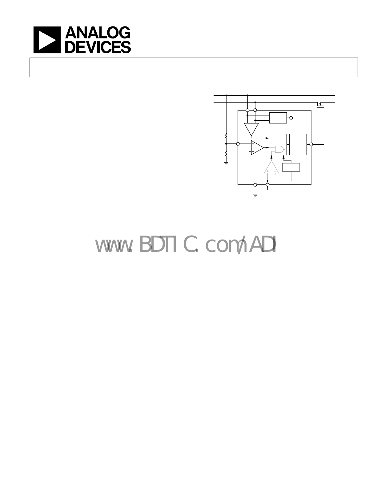
FUNCTIONAL BLOCK DIAGRAM
CC1
V
CC2
R1
SETV
R2
V
CC1
UVLO
0.618V
ADM6819/
ADM6820
GND
V
CC2
CHARGE
PUMP
LOGIC
0.618V
EN (ADM6819) - DIGITAL/ANALOG
SETD (ADM6820)
Figure 1.
V
DRIVER
TIMER
FET
FET
Q1
GATE
CC1
V
OUT
CC2
5133-001
GENERAL DESCRIPTION
The ADM6819 and ADM6820 are simple power supply sequencers
with FET drive capability for enhancing N-channel MOSFETs.
These devices can monitor a primary supply voltage and
enable/disable an external N-channel FET for a secondary
supply. The ADM6819 has the ability to monitor two supplies.
When more than two voltages require sequencing, multiple
ADM6819/ADM6820 devices can be cascaded to achieve this.
The devices operate over a supply range of 2.95 V to 5.5 V.
An internal comparator monitors the primary supply using the
V
SET pin. The input to this comparator is externally set via a
resistor divider from the primary supply. When the voltage at
the VSET pin rises above the comparator threshold, an internal
charge pump on the GATE output enhances the secondary
supply FET.
The ADM6819 features an enable (EN) pin that is fed to the
i
nput of an additional comparator and reference circuit. This
pin can be used as a digital enable or a secondary power good
comparator to monitor a second supply and enables the GATE
only if both supplies are valid. When both inputs of the internal
comparators are above the threshold, a fixed 300 ms timeout
occurs before the GATE is driven high and the secondary
supply is enabled.
The ADM6820 has only one comparator that is on the SETV
p
in. It also features a timeout period that is adjustable via a
single external capacitor on the SETD pin.
The ADM6819/ADM6820 are packaged in small 6-lead SOT-23
ckages.
pa
Rev. 0
Information furnished by Analog Devices is believed to be accurate and reliable. However, no
responsibility is assumed by Anal og Devices for its use, nor for any infringements of patents or ot her
rights of third parties that may result from its use. Specifications subject to change without notice. No
license is granted by implication or otherwise under any patent or patent rights of Analog Devices.
Trademarks and registered trademarks are the property of their respective owners.
One Technology Way, P.O. Box 9106, Norwood, MA 02062-9106, U.S.A.
Tel: 781.329.4700 www.analog.com
Fax: 781.461.3113 ©2006 Analog Devices, Inc. All rights reserved.
Page 2

ADM6819/ADM6820
www.BDTIC.com/ADI
TABLE OF CONTENTS
Features.............................................................................................. 1
Pin Configuration and Function Descriptions..............................7
Applications....................................................................................... 1
Functional Block Diagram .............................................................. 1
General Description ......................................................................... 1
Revision History ............................................................................... 2
Specifications..................................................................................... 3
Timing Diagrams.............................................................................. 4
Absolute Maximum Ratings............................................................ 6
Thermal Characteristics .............................................................. 6
ESD Caution.................................................................................. 6
REVISION HISTORY
7/06—Rev. 0: Initial Version
Typical Performance Characteristics..............................................8
Theory of Operation ...................................................................... 10
SETV Pin ..................................................................................... 10
EN Pin.......................................................................................... 10
GATE Pin .................................................................................... 10
SETD Pin..................................................................................... 10
Outline Dimensions....................................................................... 11
Ordering Guide .......................................................................... 11
Rev. 0 | Page 2 of 12
Page 3

ADM6819/ADM6820
www.BDTIC.com/ADI
SPECIFICATIONS
V
or V
CC1
= 2.95 V to 5.5 V, TA = −40°C to +85°C, unless otherwise noted. Typical values are at TA = 25°C.
CC2
Table 1.
Parameter Min Typ Max Units Conditions
V
, V
PINS V
CC1
CC2
Operating Voltage Range, V
V
or V
CC1
V
CC1
V
CC1
Supply Current, ICC 350 500 μA V
CC2
or V
Disable Mode Current 250 μA V
or V
CC2
Slew Rate
CC2
2
1.2/t
Undervoltage Lockout, V
UVLO
CC1
or V
0.9 5.5 V V
CC2
6 V/s ADM6819
V/s ADM6820
DELAY
2.4 2.525 2.65 V VCC falling
CC1
CC1
CC1
CC1
or V
CC2
or V
CC2
= V
= 3.3 V
CC2
= V
= 3.3 V, EN = GND
CC2
SETV PIN
SETV Threshold, VTH 0.602 0.618 0.634 V V
SETV Input Current
SETV Threshold Hysteresis
SETV to GATE Delay, t
2
240 300 350 ms V
DELAY
10 100 nA
−1 % V
rising, enables GATE
SETV
falling, disables GATE
SETV
> V
SETV
TH
SETD PIN ADM6820
SETD Ramp Current, I
SETD
300 500 730 nA
400 500 600 nA TA = 25°C
SETD Voltage, V
1.295 1.326 1.357 V
SETD
GATE PIN
GATE Turn-On Time, tON 0.5 1.5 10 ms C
GATE Turn-Off Time, t
GATE Voltage, V
GATE
30 μs C
OFF
4.5 5.5 6.0 V With respect to V
= 1500 pF, V
GATE
= 1500 pF, V
GATE
4.0 5.0 6 V With respect to V
8.9 9.4 9.9 V With respect to V
8.2 8.6 9.1 V With respect to V
ENABLE PIN
EN Input Voltage Low, VIL 0.4 V V
EN Input Voltage High, VIH 2.0 V V
1
100% production tested at TA = +25°C. Specifications over temperature limit are guaranteed by design.
2
Guaranteed by design, not production tested.
3
t
(s) = 2.65 × 10⁶ × C
DELAY
4
Highest supply pin is represented by V
5
Highest supply pin is represented by V
.
SET
= 2.95 V.
CCx
= 5.5 V.
CCx
CC1
CC1
or V
or V
CC2
CC2
1
must be > 2.95 V
must be > 2.95 V
3
; VEN > VTH (ADM6819)
= 3.3 V, V
CC2
= 3.3 V, V
CC2
, R
CCx
, R
CCx
, R
CCx
, R
CCx
GATE
GATE
> 50 MΩ to V
GATE
> 5 MΩ to V
GATE
> 50 MΩ to V
GATE
> 5 MΩ to V
GATE
must be > 2.95 V
must be > 2.95 V
= 7.8 V
= 0.5 V
CCx
CCx
CCx
CCx
4
4
5
5
Rev. 0 | Page 3 of 12
Page 4
ADM6819/ADM6820
V
V
www.BDTIC.com/ADI
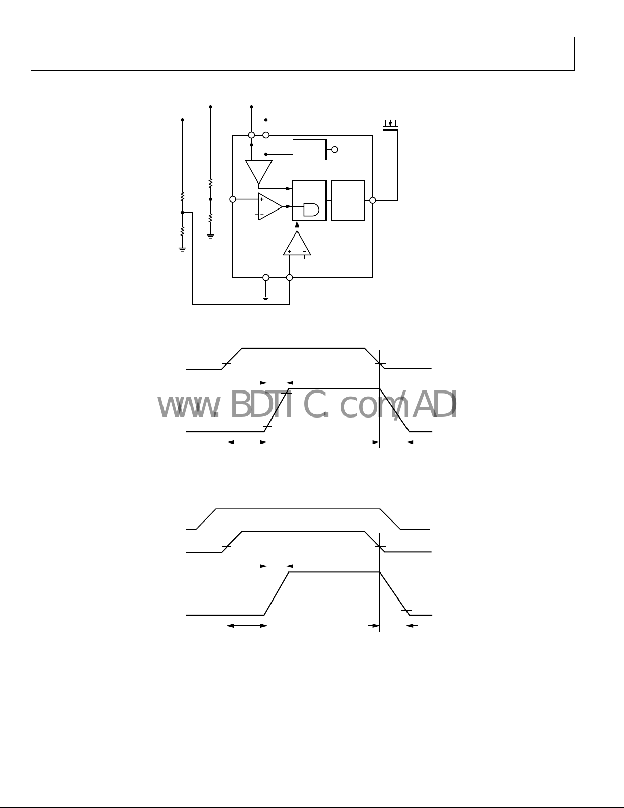
TIMING DIAGRAMS
V
CC2
CC1
Q1
V
CC1
V
CC2
CC1
V
OUT
CC2
CHARGE
PUMP
UVLO
R1
R3
R4
SETV
R2
0.618V
ADM6819
GND
LOGIC
0.618V
EN
V
FET
FET
DRIVER
GATE
05133-014
Figure 2. ADM6819 Solution for Validating Two Supplies Before Sequencing
V
SETV
V
GATE
Figure 3. ADM6819/ADM6820 Timing Diagram Using SETV for Sequencing
0.618V
t
DELAY
(ADM6819 = 300ms,
ADM6820 = ADJ)
t
ON
90%
10% 10%
V
CC2
+ 5.5V (typ)
t
OFF
05133-015
V
V
SETV
V
GATE
0.618V
EN
0.618V
t
DELAY
(300ms)
t
ON
90%
10% 10%
V
CC2
+ 5.5V (typ)
t
Figure 4. ADM6819 Timing Diagram Using EN and SETV for Sequencing
OFF
5133-016
Rev. 0 | Page 4 of 12
Page 5

ADM6819/ADM6820
V
V
V
V
V
V
www.BDTIC.com/ADI
IN
= 3.3V
IN
= 3.0V
IN
= 5
Q1
Q2
= 5
OUT
V
= 3.3V
OUT
V
= 3.0V
OUT
V
CC2
V
CC1
R1
SETV
R2
GATE
ADM6819/
ADM6820
EN/SETD
GND
R3
R4
V
CC2
V
CC1
ADM6819/
ADM6820
SETV
GND
GATE
EN/SETD
05133-017
Figure 5. ADM6819/ADM6820 Solution for Sequencing Three Supply Rails
Rev. 0 | Page 5 of 12
Page 6

ADM6819/ADM6820
www.BDTIC.com/ADI
ABSOLUTE MAXIMUM RATINGS
Table 2.
Parameter Rating
V
, V
−0.3 V to +6.0 V
CC1
CC2
SETV, SETD, EN −0.3 V to +30 V
GATE −0.3 V to (V
Storage Temperature −65°C to +150°C
Operating Temperature Range −40°C to +85°C
Lead Temperature (Soldering 10 sec) 300°C
Junction Temperature 150°C
+ 11 V)
CCx
ESD CAUTION
ESD (electrostatic discharge) sensitive device. Electrostatic charges as high as 4000 V readily accumulate on
the human body and test equipment and can discharge without detection. Although this product features
proprietary ESD protection circuitry, permanent damage may occur on devices subjected to high energy
electrostatic discharges. Therefore, proper ESD precautions are recommended to avoid performance
degradation or loss of functionality.
Stresses above those listed under Absolute Maximum Ratings
ma
y cause permanent damage to the device. This is a stress
rating only; functional operation of the device at these or any
other conditions above those indicated in the operational
section of this specification is not implied. Exposure to absolute
maximum rating conditions for extended periods may affect
device reliability.
THERMAL CHARACTERISTICS
θJA is specified for the worst-case conditions, that is, a device
soldered in a circuit board for surface-mount packages.
Table 3. Thermal Resistance
Package Type θJA Unit
6-Lead SOT-23 169.5 °C/W
Rev. 0 | Page 6 of 12
Page 7

ADM6819/ADM6820
SETV
SETV
www.BDTIC.com/ADI
PIN CONFIGURATION AND FUNCTION DESCRIPTIONS
V
CC1
GND
1
ADM6819
2
TOP VIEW
(Not to S cale)
3
6
5
4
V
CC2
GATE
EN
05133-002
Figure 6. ADM6819 Pin Configuration
Table 4. Pin Function Descriptions
Pin Number
ADM6819 ADM6820
1 1 V
Mnemonic Description
CC1
Supply Voltage 1. Either V
CC1
FET Drive.
2 2 GND Chip Ground Pin.
3 3 SETV
Sequenced Threshold Set. Connect to an external resistor divider to set the V
threshold that enables GATE turn-on. The internal reference is 0.618 V.
4 – EN
Active-High Enable. GATE drive is enabled t
immediately disabled when EN is driven low. Connect this pin to the higher of V
if not used. EN is internally identical to SETV (0.618 V threshold) and, therefore, can
V
CC2
be used as a second supply monitor, enabling two supplies to be validated before
sequencing begins.
– 4 SETD
5 5 GATE
GATE Delay Set Input. Connect an external capacitor from SETD to GND to adjust the
y from SETV > V
dela
to GATE turn-on. t
TH
GATE Drive Output. GATE drives an external N-channel FET to connect V
GATE drive enables t
after SETV exceeds V
DELAY
immediately disabled when SETV drops below V
enabled, an internal charge pump drives GATE above V
N-channel FET.
6 6 V
CC2
Supply Voltage 2. Either V
CC1
external FET Drive.
V
CC1
GND
1
ADM6820
2
TOP VIEW
(Not to S cale)
3
6
5
4
V
CC2
GATE
SETD
05133-003
Figure 7. ADM6820 Pin Configuration
or V
must be greater than the UVLO to enable external
CC2
after EN is driven high. GATE drive is
DELAY
(s) = 2.652 × 10⁶ × C
DELAY
and ENABLE is driven high. GATE drive is
TH
or ENABLE is driven low. When
TH
or V
must be greater than the UVLO to enable the
CC2
to fully enhance the external
CCX
SET
(F).
to the load.
CC2
CC1
or
CC1
Rev. 0 | Page 7 of 12
Page 8

ADM6819/ADM6820
www.BDTIC.com/ADI
TYPICAL PERFORMANCE CHARACTERISTICS
0.50
0.65
0.45
I
(V
= 3.3V, V
CC2
0.40
0.35
0.30
0.25
SUPPLY CURRENT (mA)
0.20
0.15
0.10
–25 0 25 50 75 100 125
–50
CC1
I
(V
= 5V, V
CC1
CC1
TEMPERATURE (° C)
CC2
CC2
= 3.3V)
= 5V)
VEN = 2V
V
= 2V
SETV
150
05133-004
Figure 8. Supply Current vs. Temperature
0.50
V
= 0V
CC1
0.45
V
= 2V
EN
V
= 2V
SETV
0.40
0.35
0.30
(mA)
0.25
CC2
I
0.20
0.15
0.10
0.05
0
0.50
0.45
0.40
0.35
0.30
(mA)
0.25
CC2
I
0.20
0.15
0.10
0.05
0
123456
0
V
(V)
CC2
vs. V
CC2
(V)
vs. V
CC2
CC2
Figure 9. I
V
= 3.3V
CC1
V
= 2V
EN
V
= 2V
SETV
123456
0
CC2
V
CC2
Figure 10. I
7
05133-005
7
05133-006
0.64
0.63
0.62
0.61
0.60
SUPPLY CURRENT (mA)
0.59
0.58
–50 150
–25 0 25 50 75 100 125
TEMPERATURE (°C)
05133-007
Figure 11. Supply Current vs. Temperature
14
12
10
(V)
8
GATE
V
6
4
V
2
0
06
14
12
10
(V)
8
GATE
V
6
4
2
0
06
12345
V
(V)
CC2
Figure 12. V
12345
Figure 13. V
vs. V
(V)
vs. V
CC2
CC2
GATE
V
CC2
GATE
V
V
CC1
EN
SETV
V
V
V
= 3.3V
= 2V
= V
CC1
= 2V
EN
SETV
= 0V
= 1V
CC2
05133-008
05133-009
Rev. 0 | Page 8 of 12
Page 9

ADM6819/ADM6820
5
5
www.BDTIC.com/ADI
14
12
10
(V)
8
GATE
V
6
4
V
2
0
06
12345
V
(V)
CC2
vs. V
Figure 14. V
340
330
320
310
300
(ms)
290
DELAY
280
t
270
260
250
240
–25 0 25 50 75 100 125
–50 150
Figure 15. t
GATE
TEMPERATURE (°C)
vs. Temperature
DELAY
CC2
V
V
CC1
EN
SETV
= 3.3V
= 2V
= 1V
05133-010
05133-011
V
V
V/DIV
V
GATE
V/DIV
SETV
GATE
20µs/DIV
Figure 16. Gate Turn-Off Time
1ms/DIV
Figure 17. Gate Turn-On Time
C
C
LOAD
LOAD
= 1500pF
= 1500pF
5133-018
5133-019
Rev. 0 | Page 9 of 12
Page 10

ADM6819/ADM6820
V
V
V
V
V
V
V
V
www.BDTIC.com/ADI
THEORY OF OPERATION
The ADM6819/ADM6820 provide local voltage sequencing in
multisupply systems. Figure 18 and Figure 19 show typical
plication diagrams for these devices.
ap
= 3.3
IN
VIN = 3.0V V
V
CC2
V
CC1
R1
SETV
R2
Figure 18. ADM6819 Applications Diagram
= 3.3
IN
VIN = 3.0V V
V
CC2
V
CC1
R1
SETV
R2
Figure 19. ADM6820 Applications Diagram
GATE
ADM6819
GND
GATE
ADM6820
SETD
GND
EN
Q1
Q1
ON
C
SET
OFF
OUT
OUT
OUT
OUT
= 3.3
= 3.0V
= 3.3
= 3.0V
SETV PIN
The ADM6819/ADM6820 enable a supply after a monitored
supply voltage exceeds a programmed threshold. This threshold
is programmed by a R1/R2 resistor divider on the SETV pin.
Once the voltage on SETV exceeds the 0.618 V threshold, the
FET switches on after the delay timer expires. On the
ADM6820, this delay is programmable using a capacitor on the
SETD pin. On the ADM6819, this delay is fixed at 300 ms and
the EN pin must be valid high to begin the timer. The required
turn-on voltage is calculated by the following equation:
R1 =
R2 ((VTRIP/V
TH
) – 1)
where:
VT
05133-012
RIP is the minimum turn-on voltage at the supply being
monitored.
V
= 0.618 V.
TH
High value resistors can be used because the SETV input
current is typically 10 nA.
EN PIN
The ADM6819 has an enable (EN) pin connected to the input
of a second comparator, which is identical to that on the VSET
pin. EN can be used as a digital input provided the signal V
below 0.6 V. Alternatively, the enable input can be used to
validate a second supply. The fixed 300 ms timer does not begin
05133-013
counting until both SETV and EN are above the threshold. As a
result, the output is not enabled until this timer has expired.
is
OL
When the primary supply is above the desired threshold, the
ADM6819/ADM6820 are designed to control the N-channel
FET in the secondary power path to enable the secondary
supply. The GATE pin is held low while both V
CC1
and V
CC2
are
below the undervoltage threshold, ensuring that the FET is held
off. When V
CC1
or V
is above UVLO and the primary supply
CC2
is above the desired level dictated by the resistor divider to the
VSET pin, the external FET is driven on after the delay has
expired. An internal charge pump enhances the external FET. A
FET with a low drain-source resistance and low V
should be
TH
chosen to reduce voltage drop across the drain-source when the
FET is fully enhanced. Either supply may act as the primary
source if V
capacitor of typically 100 nF should be used on whichever V
CC1
or V
is greater that 2.95 V. A decoupling
CC2
CC
is the main supply.
GATE PIN
The internal charge pump is capable of driving the gate of an
N-channel MOSFET with no external capacitors. This ensures
that the MOSFET is enhanced to provide a minimum voltage
drop across the MOSFET, thus reducing the voltage drop across
the FET. This charge pump is designed to drive the high impedance capacitive load of a MOSFET gate input. The GATE pin
should not be resistively loaded because it reduces the gate drive
capability. During undervoltage lockout, GATE is held to GND.
SETD PIN
The ADM6820 features a capacitor adjustable sequencing delay.
A capacitor connected to the SETD pin determines the length
of the sequencing delay. The sequencing delay can be calculated
by the following equation:
t
(s) = 2.652 × 10⁶ × CSET
DELAY
The ADM6819 has a fixed 300 ms delay.
Rev. 0 | Page 10 of 12
Page 11

ADM6819/ADM6820
www.BDTIC.com/ADI
OUTLINE DIMENSIONS
2.90 BSC
45
2.80 BSC
2
0.95 BSC
1.90
BSC
1.45 MAX
0.50
0.30
Dim
ensions shown in millimeters
SEATING
PLANE
(RJ-6)
0.22
0.08
10°
4°
0°
0.60
0.45
0.30
1.60 BSC
PIN 1
INDICATOR
1.30
1.15
0.90
0.15 MAX
6
1 3
COMPLIANT TO JEDEC STANDARDS MO-178-AB
Figure 20. 6-Lead Small Outline Transistor Package [SOT-23]
ORDERING GUIDE
Model Temperature Range Package Description Package Option Branding
ADM6819ARJZ-REEL7
ADM6820ARJZ-REEL7
1
Z = Pb-free part.
1
−40°C to +85°C
1
−40°C to +85°C
6-Lead Small Outline Transistor Package [SOT-23] RJ-6 M2R
6-Lead Small Outline Transistor Package [SOT-23] RJ-6 M2S
Rev. 0 | Page 11 of 12
Page 12

ADM6819/ADM6820
www.BDTIC.com/ADI
NOTES
©2006 Analog Devices, Inc. All rights reserved. Trademarks and
registered trademarks are the property of their respective owners.
D05113-0-7/06(0)
Rev. 0 | Page 12 of 12
 Loading...