

Page 1
Tri-Mode: +3.3 V, +5 V, Adjustable
a
Micropower Linear Voltage Regulators
FEATURES
Tri-Mode Operation
3.3 V, 5 V Fixed or +1.3 V to +16 V Adjustable
Low Power CMOS: 9 µA max Quiescent Current
High Current 100 mA Output
Low Dropout Voltage
Upgrade for ADM663/ADM666
“Small” 0.1 µF Output Capacitor (0805 Style)
+2 V to +16.5 V Operating Range
Low Battery Detector ADM666A
No Overshoot on Power-Up
Thermal Shutdown
APPLICATIONS
Handheld Instruments
LCD Display Systems
Pagers
Battery Operated Equipment
GENERAL DESCRIPTION
The ADM663A/ADM666A are precision linear voltage regulators featuring a maximum quiescent current of 9 µA. They can
be used to give a fixed +3.3 V or +5 V output with no additional
external components or can be adjusted from 1.3 V to 16 V
using two external resistors. Fixed or adjustable operation is automatically selected via the V
input. The low quiescent cur-
SET
rent makes these devices especially suitable for battery powered
systems. The input voltage range is 2 V to 16.5 V, and an output current up to 100 mA is provided. Current limiting may be
set using a single external resistor. For additional safety, an
internal thermal shutdown circuit monitors the internal die
temperature.
The ADM666A features additional low battery monitoring circuitry to detect for low battery voltages.
The ADM663A/ADM666A are pin compatible enhancements
for the ADM663/ADM666. Improvements include an additional 3.3 V output range, higher output current, and operation
with a small output capacitor.
The ADM663A/ADM666A are available in an 8-pin DIP and
narrow surface mount (SOIC) packages.
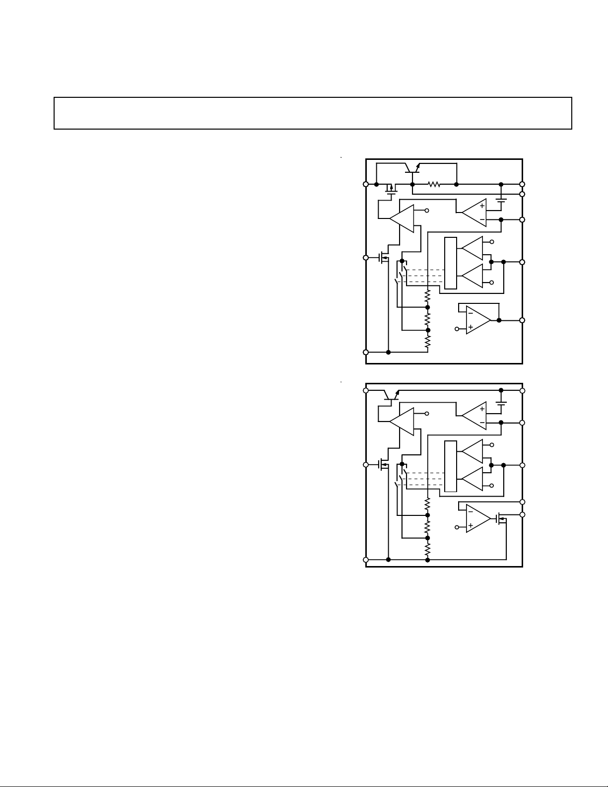
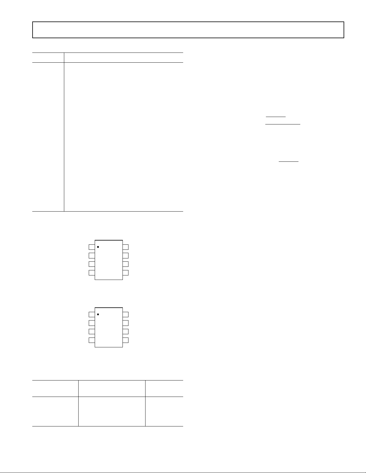
ADM663A/ADM666A*
FUNCTIONAL BLOCK DIAGRAMS
V
IN
1.3V
A1
D
E
1.3 V
C
O
D
E
R
0.9V
ADM663A
D
E
C
O
D
E
R
1.3V
ADM666A
SHDN
GND
V
SHDN
GND
R1
R2
R3
IN
A1
R1
R2
R3
C1
C2
C3
A2
C1
C2
C3
C4
VIN–50mV
50mV
VIN–50mV
50mV
0.5V
0.5V
V
OUT2
V
OUT1
SENSE
V
SET
V
TC
V
OUT
SENSE
V
SET
LBI
LBO
*Patent pending.
REV. 0
Information furnished by Analog Devices is believed to be accurate and
reliable. However, no responsibility is assumed by Analog Devices for its
use, nor for any infringements of patents or other rights of third parties
which may result from its use. No license is granted by implication or
otherwise under any patent or patent rights of Analog Devices.
One Technology Way, P.O. Box 9106, Norwood. MA 02062-9106, U.S.A.
Tel: 617/329-4700 Fax: 617/326-8703
Page 2

ADM663A/ADM666A–SPECIFICATIONS
(VIN = +9 V, TA = T
MIN
to T
, unless otherwise noted)
MAX
Parameter Min Typ Max Units Test Conditions/Comments
Input Voltage, V
Quiescent Current, I
Output Voltage, V
Output Voltage, V
Dropout Voltage, V
Dropout Voltage, V
Line Regulation (∆V
IN
Q
(+5 V Mode) 4.75 5.0 5.25 V V
OUT(2)
(+3.3 V Mode) 3.135 3.3 3.465 V V
OUT(2)
DO
DO
/∆VIN) 0.03 0.35 %/V +2 V ≤ VIN ≤ +15 V, V
OUT(2)
Load Regulation VIN = (V
∆V
∆V
Reference Voltage, V
Reference Tempco (∆V
V
SET
V
F/A
V
F/A
V
SET
Shutdown Input Voltage, V
Shutdown Input Current, I
SENSE Input Threshold, V
SENSE Input Resistance, R
Input-Output Saturation Resistance, R
ADM663A, V
Output Current, I
Minimum Load Current, I
OUT(2)
OUT1
;(∆V
;(∆V
OUT(2)
OUT1
/∆I
/∆I
OUT1
SET
) 0.3 1.0 Ω V
OUT(2)
) 0.25 1.2 Ω ADM663A, 50 µA ≤ I
/∆T) ±100 ppm/°C
SET
Internal Threshold
Low 50 mV V
High VIN – 50 mV V
Input Current, I
OUT1
OUT(2)
SET
SHDN
SHDN
OUT
SENSE
L (MIN)
– V
SENSE
SAT
2.0 16.5 V
69 µA No Load, V
0.75 0.9 V I
1.0 1.2 V I
0.15 0.35 Ω V
0.15 0.30 Ω V
1.27 1.33 V T
= GND
SET
= V
SET
= 40 mA, V
OUT
= 100 mA, V
OUT
= GND (Fixed +5 V Output)
SET
= VIN (Fixed +3.3 V Output)
SET
= Resistive Divider (Adjustable Output)
SET
= +25°C, V
A
< V
SET
> V
SET
= +16.5 V
IN
IN
+3 V), 1 mA ≤ I
OUT
Low for +5 V Output
F/A
High for +3.3 V Output
F/A
OUT
OUT
OUT
= V
= +14.5 V
= +14.5 V
OUT
OUT1
SET
±0.01 ±10 nA
1.4 V V
0.3 V V
High = Output Off
SHDN
Low = Output On
SHDN
±0.01 ±10 nA
0.5 V Current Limit Threshold
3MΩ
200 400 Ω V
20 40 Ω V
20 30 Ω V
= +2 V, I
IN
= +9 V, I
IN
= +15 V, I
IN
= 1 mA
OUT
= 10 mA
OUT
OUT
= 10 mA
100 mA +3 V ≤ VIN ≤ +16.5 V, V
1.0 µA
IN
LBI Input Threshold
Low Going 1.1 1.26 V ADM666A
High Going 1.29 1.42 V ADM666A
Hysteresis 30 mV ADM666A
LBI Input Current, I
LBO Output Saturation Resistance, R
LBI
SAT
±0.01 ±10 nA ADM666A
20 30 Ω ADM666A, I
= 2 mA
SAT
LBO Output Leakage Current 0.2 nA ADM666A, LBI = 1.4 V
V
Open Circuit Voltage, V
TC
V
Sink Current, I
TC
V
Temperature Coefficient +2.5 mV/°C ADM663A
TC
Specifications subject to change without notice.
TC
TC
0.9 V ADM663A
8.0 2.0 mA ADM663A
= V
REF
OUT(2)
≤ 10 mA
– V
= +1.5 V
OUT
≤ 100 mA
ABSOLUTE MAXIMUM RATINGS*
(TA = +25°C unless otherwise noted)
Input Voltage, VIN . . . . . . . . . . . . . . . . . . . . . . . . . . . . . +18 V
Terminal Voltage
(ADM663A) Pins 1, 3, 5, 6, 7
. . . . . . . . . . . . . . . . . . . . . . (GND
– 0.3 V) to (VIN + 0.3 V)
(ADM666A) Pins 1, 2, 3, 5, 6
. . . . . . . . . . . . . . . . . . . . . . . (GND
(ADM663A) Pin 2 . . . . . . . . (GND – 0.3 V) to (V
(ADM666A) Pin 7 . . . . . . . . . . . . . . (GND
– 0.3 V) to (VIN + 0.3 V)
– 0.3 V) to +16.5 V
OUT1
+ 0.3 V)
Output Source Current
(ADM663A, ADM666A) Pin 2 . . . . . . . . . . . . . . . . . . 100 mA
(ADM663A) Pin 3 . . . . . . . . . . . . . . . . . . . . . . . . . . . . . 25 mA
Output Sink Current, Pin 7 . . . . . . . . . . . . . . . . . . . . . .–20 mA
Power Dissipation, N-8 . . . . . . . . . . . . . . . . . . . . . . . . 800 mW
(Derate 8.3 mW/°C above +30°C)
θ
, Thermal Impedance . . . . . . . . . . . . . . . . . . . . . . 120°C/W
JA
Power Dissipation, R-8 . . . . . . . . . . . . . . . . . . . . . . . .570 mW
(Derate 6 mW/°C above +30°C)
θ
, Thermal Impedance . . . . . . . . . . . . . . . . . . . . . 170°C/W
JA
Operating Temperature Range
Industrial (A Version) . . . . . . . . . . . . . . . . . –40°C to +85°C
Storage Temperature Range . . . . . . . . . . . . –65°C to +150°C
Lead Temperature (Soldering, 10 sec) . . . . . . . . . . . . . +300°C
Vapor Phase (60 sec) . . . . . . . . . . . . . . . . . . . . . . . . +215°C
Infrared (15 sec) . . . . . . . . . . . . . . . . . . . . . . . . . . . . +220°C
ESD Rating . . . . . . . . . . . . . . . . . . . . . . . . . . . . . . . . .>5000 V
*This is a stress rating only and functional operation of the device at these or any
other conditions above those indicated in the operation sections of this specification is not implied. Exposure to absolute maximum rating conditions for extended
periods of time may affect reliability.
–2–
REV. 0
Page 3
ADM663A/ADM666A
PIN FUNCTION DESCRIPTION
Mnemonic Function
V
OUT(1) (2)
V
IN
Voltage Regulator Output(s).
Voltage Regulator Input.
SENSE Current Limit Sense Input. (Referenced to
V
V
) If not used, it should be connected to
OUT(2).
OUT(2).
GND Ground Pin. Must be connected to 0 V.
LBI Low Battery Detect Input. Compared with 1.3 V.
LBO Low Battery Detect Output. Open Drain Output.
SHDN Digital Input. May be used to disable the device
so that the power consumption is minimized.
V
SET
Voltage Setting Input. Connect to GND for
+5 V output, to V
for +3.3 V output or
IN
connect to external resistive divider for
adjustable output.
V
TC
Temperature-Proportional Voltage for negative
TC Output.
PIN CONFIGURATIONS
DIP & SOIC
SENSE
V
OUT2
V
OUT1
GND
1
2
ADM663A
TOP VIEW
3
(Not to Scale)
4
V
8
IN
7
V
TC
6
V
SET
5
SHDN
DIP & SOIC
TERMINOLOGY
Dropout Voltage: The input/output voltage differential at
which the regulator no longer maintains regulation against further reductions in input voltage. It is measured when the output
decreases 100 mV from its nominal value. The nominal value is
the measured value with V
IN
= V
OUT
+2 V.
Line Regulation: The change in output voltage as a result of
a change in the input voltage. It is specified as a percentage
change in output voltage for an input voltage change.
∆V
OUT
Line Reg =
V
OUT
∆V
(100)
IN
Load Regulation: The change in output voltage for a change
in output current.
∆V
Load Reg (Ω) =
∆I
OUT
OUT
Quiescent Current: The input bias current which flows when
the regulator output is unloaded or when the regulator is in
shutdown.
Sense Input Threshold: Current limit sense voltage. This
is the voltage (referenced to V
) at which current limiting
OUT(2)
occurs.
Input-Output Saturation Resistance (ADM663A): This is a
measure of the internal MOS transistor effective resistance in series with V
. The minimum input-output voltage differential
OUT1
at low currents may be calculated by multiplying the load current by the saturation resistance.
Thermal Limiting: This feature monitors the internal die temperature and disables the output when an internal temperature
of 125°C is reached.
Maximum Power Dissipation: The maximum total device
dissipation for which the regulator will continue to operate
within specifications.
SENSE
V
OUT
LBI
GND
1
2
ADM666A
TOP VIEW
3
(Not to Scale)
4
8
V
IN
7
LBO
6
V
SET
5
SHDN
ORDERING GUIDE
Temperature Package
Model Range Option
ADM663AAN –40°C to +85°C N-8
ADM663AAR –40°C to +85°C R-8
ADM666AAN –40°C to +85°C N-8
ADM666AAR –40°C to +85°C R-8
REV. 0
–3–
Page 4

ADM663A/ADM666A
GND
ADM663A
ADM666A
SENSE
V
OUT(2)
V
IN
V
SET
SHDN
+3.3V
OUTPUT
+4.5V TO +16V
INPUT
GENERAL INFORMATION
The ADM663A/ADM666A contains a micropower bandgap
reference voltage source; an error amplifier, A1; three comparators, C1, C2, C3, and a series pass output transistor. A P-channel FET and an NPN transistor are used on the ADM663A
while the ADM666A uses an NPN output transistor.
CIRCUIT DESCRIPTION
The internal bandgap reference is trimmed to 1.3 V ± 30 mV.
This is used as a reference input to the error amplifier A1. The
feedback signal from the regulator output is supplied to the
other input by an on-chip voltage divider or by two external resistors. When V
is at ground, the internal divider tap between
SET
R1 and R2, provides the error amplifier’s feedback signal giving
a +5 V output. When V
is at VIN, the internal divider tap be-
SET
tween R2 and R3 provides the error amplifier’s feedback signal
giving a +3.3 V output. When V
above ground and less than 50 mV below V
fier’s input is switched directly to the V
is at more than 50 mV
SET
, the error ampli-
IN
pin, and external
SET
resistors are used to set the output voltage. The external resistors are selected so that the desired output voltage gives 1.3 V
at V
.
SET
Comparator C1 monitors the output current via the SENSE input. This input, referenced to V
, monitors the voltage
OUT(2)
drop across a load sense resistor. If the voltage drop exceeds
0.5 V, then the error amplifier A1 is disabled and the output
current is limited.
The ADM663A has an additional amplifier, A2, which provides
a temperature proportional output, V
. If this is summed into
TC
the inverting input of the error amplifier, a negative temperature
coefficient results at the output. This is useful when powering
liquid crystal displays over wide temperature ranges.
The ADM666A has an additional comparator, C4, that compares the voltage on the low battery input, LBI, pin to the internal +1.3 V reference. The output from the comparator drives an
open drain FET connected to the low battery output pin, LBO.
The low battery threshold may be set using a suitable voltage
divider connected to LBI. When the voltage on LBI falls below
1.3 V, the open drain output LBO is pulled low.
Both the ADM663A and the ADM666A contain a shutdown
(SHDN) input that can be used to disable the error amplifier
and hence the voltage output. The power consumption in shutdown reduces to less than 9 µA.
V
SHDN
GND
IN
A1
1.3 V
R1
R2
R3
D
E
C
O
D
E
R
1.3V
ADM666A
C1
C2
C3
C4
VIN–50mV
50mV
0.5V
V
OUT
SENSE
V
SET
LBI
LBO
Figure 2. ADM666A Functional Block Diagram
Circuit Configurations
For a fixed +5 V output the V
input is grounded and no ex-
SET
ternal resistors are necessary. This basic configuration is shown
in Figure 3. For a fixed +3.3 V output, the V
nected to V
as shown in Figure 4. Current limiting is not be-
IN
ing utilized so the SENSE input is connected to V
GND
SENSE
V
OUT(2)
SHDN
+6V TO +16V
INPUT
V
IN
ADM663A
ADM666A
V
SET
input is con-
SET
OUT(2)
+5V
OUTPUT
.
Figure 3. A Fixed +5 V Output
V
IN
1.3V
A1
SHDN
R1
R2
R3
GND
Figure 1. ADM663A Functional Block Diagram
D
E
C
O
D
E
R
0.9V
C1
VIN–50mV
C2
C3
50mV
A2
ADM663A
V
V
0.5V
OUT2
OUT1
SENSE
V
SET
V
TC
Figure 4. A Fixed +3.3 V Output
Output Voltage Setting
If V
is not connected to GND or to VIN, the output voltage is
SET
set according to the following equation:
V
OUT=VSET
where V
= 1.30 V.
SET
–4–
(R1+ R2)
×
R1
REV. 0
Page 5

ADM663A/ADM666A
ADM666A
SENSE
V
OUT
GND
V
IN
V
SET
LBI
+1.3V TO +15V
OUTPUT
+2V TO +16V
INPUT
R
CL
R2
R1
LBO
SHDN
R3
R4
LOW
BATTERY
OUTPUT
The resistor values may be selected by first choosing a value for
R1 and then selecting R2 according to the following equation:
R2 = R1×
The input leakage current on V
SET
V
1. 3 0
is 10 nA maximum. This al-
OUT
− 1
lows large resistor values to be chosen for R1 and R2 with little
degradation in accuracy. For example, a 1 MΩ resistor may be
selected for R1, and then R2 may be calculated accordingly.
The tolerance on V
is guaranteed at less than ±30 mV so in
SET
most applications, fixed resistors will be suitable.
GND
SENSE
V
OUT(2)
V
SET
R
CL
+1.3V TO +15V
OUTPUT
R2
R1
+2V TO +16V
INPUT
V
IN
ADM663A
ADM666A
SHDN
Figure 5. Adjustable Output
Table I. Output Voltage Selection
the current drain to a low quiescent (9 µA maximum) current.
This is very useful for low power applications. The SHDN input
should be driven with a CMOS logic level signal since the input
threshold is 0.3 V. In TTL systems, an open collector driver
with a pull-up resistor may be used.
If the shutdown function is not being used, then it should be
connected to GND.
Low Supply or Low Battery Detection
The ADM666A contains on-chip circuitry for low power supply
or battery detection. If the voltage on the LBI pin falls below the
internal 1.3 V reference, then the open drain output LBO will
go low. The low threshold voltage may be set to any voltage
above 1.3 V by appropriate resistor divider selection.
V
R3 = R4
BATT
1. 3 V
where R3 and R4 are the resistive divider resistors and V
− 1
is
BATT
the desired low voltage threshold.
Since the LBI input leakage current is less than 10 nA, large val-
ues may be selected for R3 and R4 in order to minimize loading.
For example, a 6 V low threshold may be set using 10 MΩ for
R3 and 2.7 M Ω for R4.
V
SET
V
OUT
GND +5 V
V
IN
+3 V
R1/R2 ADJ
Current Limiting
Current limiting may be achieved by using an external current
sense resistor in series with V
. When the voltage across
OUT(2)
the sense resistor exceeds the internal 0.5 V threshold, current
limiting is activated. The sense resistor is therefore chosen such
that the voltage across it will be 0.5 V when the desired current
limit is reached.
0.5
RCL=
I
CL
where RCL is the current sense resistor, ICL is the maximum
current limit.
The value chosen for R
should also ensure that the current is
CL
limited to less than the 100 mA absolute maximum rating and
also that the power dissipation will also be within the package
maximum ratings.
If current limiting is employed, there will be an additional voltage drop across the sense resistor that must be considered when
determining the regulators dropout voltage.
If current limiting is not used, the SENSE input should be connected to V
OUT(2)
.
Shutdown Input (SHDN)
The SHDN input allows the regulator to be turned off with a
logic level signal. This will disable the output and reduce
REV. 0
Figure 6. ADM666A Adjustable Output with Low Battery
Detection
High Current Operation
The ADM663A contains an additional output, V
OUT1
, suitable
for directly driving the base of an external NPN transistor. Figure 7 shows a configuration which can be used to provide +5 V
with boosted current drive. A 1 Ω current sensing resistor limits
the current at 0.5 A.
V
IN
V
10µF
SHUTDOWN
+
IN
ADM663A
SHD N
V
SET
GND
V
OUT1
V
OUT2
SENSE
10µF
100Ω
+
2N4237
1.0Ω
+5V, 0.5A
OUTPUT
Figure 7. ADM663A Boosted Output Current (0.5 A)
–5–
Page 6

ADM663A/ADM666A
Temperature Proportional Output
The ADM663A contains a VTC output with a positive temperature coefficient of +2.5 mV/°C. This may be connected to the
summing junction of the error amplifier (V
) through a resis-
SET
tor resulting in a negative temperature coefficient at the output
of the regulator. This is especially useful in multiplexed LCD
displays to compensate for the inherent negative temperature
coefficient of the LCD threshold. At +25°C the voltage at the
VTC output is typically 0.9 V. The equations for setting both
the output voltage and the tempco are given below. If this function is not being used, then V
V
OUT=VSET
TCV
OUT
SENSE
V
where V
= +1.3 V, VTC = +0.9 V, TCV
SET
ADM663A
should be left unconnected.
TC
OUT2
V
1+
SET
V
R2
R2
V
+
R1
–R2
=
R3
TC
()
SET−VTC
R3
TCV
()
TC
= +2.5 mV/°C
TC
R2
R1
R3
V
OUT
Figure 8. ADM663A Temperature Proportional Output
APPLICATION HINTS
Input-Output (Dropout Voltage)
A regulator’s minimum input-output differential or dropout
voltage determines the lowest input voltage for a particular output voltage. The ADM663A/ADM666A dropout voltage is 1 V
at its rated output current. For example when used as a fixed
+5 V regulator, the minimum input voltage is +6 V. At lower
output currents (I
< 10 mA) on the ADM663A, V
OUT
OUT1
may
be used as the output driver in order to achieve lower dropout
voltages. In this case the dropout voltage depends on the voltage
drop across the internal FET transistor. This may be calculated
by multiplying the FET’s saturation resistance by the output
current, for example with V
= 9 V, R
IN
= 20 Ω. Therefore,
SAT
the dropout voltage for 5 mA is 100 mV. As the current limit
circuitry is referenced to V
V
. For high current operation V
OUT1
and V
left unconnected.
OUT1
+6V TO +16V
INPUT
OUT2
V
IN
ADM663A
V
SET
, V
should be connected to
OUT2
should be used alone
OUT2
SENSE
V
OUT2
V
GND
OUT1
SHDN
+5V
OUTPUT
Figure 9. Low Current, Low Dropout Configuration
Thermal Considerations
The ADM663A/ADM666A can supply up to 100 mA load current and can operate with input voltages up to 16.5 V, but the
package power dissipation and hence the die temperature must
be kept within the maximum limits. The package power dissipation is calculated from the product of the voltage differential
across the regulator times the current being supplied to the load.
The power dissipation must be kept within the maximum limits
given in the Absolute Maximum Ratings section.
P
= (VIN–V
D
OUT
)(IL)
The die temperature is dependent on both the ambient temperature and on the power being dissipated by the device. The
ADM663A/ADM666A contains an internal thermal limiting circuit which will shut down the regulator if the internal die temperature exceeds 125°C. Therefore, care must be taken to
ensure that, under normal operating conditions, the die temperature is kept below the thermal limit.
T
= TA + PD (
J
θ
)
JA
This may be expressed in terms of power dissipation as follows:
= (TJ – TA)/(
P
D
θ
)
JA
where:
= Die Junction Temperature (°C)
T
J
= Ambient Temperature (°C)
T
A
= Power Dissipation (W)
P
D
θ
= Junction to Ambient Thermal Resistance (°C/W)
JA
If the device is being operated at the maximum permitted ambient temperature of 85°C the maximum power dissipation permitted is:
P
(max) = (TJ (max) – TA)/(
D
(max) = (125 – 85)/(θ
P
D
θ
= 40/
JA
θ
= 120°C/W for the 8-pin DIP (N-8) package
JA
θ
= 170°C/W for the 8-pin SOIC (R-8) package
JA
θ
)
JA
)
JA
Therefore, for a maximum ambient temperature of 85°C
(max) = 333 mW for N-8
P
D
(max) = 235 mW for R-8
P
D
At lower ambient temperatures the maximum permitted power
dissipation increases accordingly up to the maximum limits
specified in the absolute maximum specifications.
The thermal impedance (θ
) figures given are measured in still
JA
air conditions and are reduced considerably where fan assisted
cooling is employed. Other techniques for reducing the thermal
impedance include large contact pads on the printed circuit
board and wide traces. The copper will act as a heat exchanger
thereby reducing the effective thermal impedance.
High Power Dissipation Recommendations
Where excessive power dissipation due to high input-output differential voltages and or high current conditions exists, the simplest method of reducing the power requirements on the
regulator is to use a series dropper resistor. In this way the excess power can be dissipated in the external resistor. As an example, consider an input voltage of +12 V and an output
voltage requirement of +5 V @ 100 mA with an ambient temperature of +85°C. The package power dissipation under these
conditions is 700 mW which exceeds the maximum ratings. By
using a dropper resistor to drop 4 V, the power dissipation requirement for the regulator is reduced to 300 mW which is
within the maximum specifications for the N-8 package at
–6–
REV. 0
Page 7

ADM663A/ADM666A
5010
0
1.0
0
0.3
0.1
0.2
0.6
0.4
0.5
0.7
0.8
0.9
403020
I
OUT2
– mA
|V
IN
– V
OUT
| – Volts
VIN = +2V
TA = +25°C
VIN = +9V
VIN = +15V
+85°C. The resistor value is calculated as R = 4/0.1 = 40 Ω. A
resistor power rating of 400 mW or greater may be used.
Bypass Capacitors
The high frequency performance of the ADM663A/ADM666A
may be improved by decoupling the ouput using a filter capacitor. A capacitor of 0.1 µF is suitable.
Typical Performance Characteristics
80
60
40
PSRR – dB
20
0
0.01 0.1 100001000100101
FREQUENCY – Hz
VINDC = +9V
V
p-p = +2V
IN
V
DC = +5V
OUT
TA = +25°C
An input capacitor helps reduce noise, improves dynamic performance and reduces the input dV/dt at the regulator input. A
suitable input capacitor is 0.1 µF or greater.
12
TA = +25°C
10
8
6
– µA
IN
I
4
2
0
4
2
V
– Volts
IN
V
= +5V
OUT
V
= +3.3V
OUT
14108612
16
Figure 10. Power Supply Rejection Ratio vs. Frequency
2.0
1.8
1.6
1.4
1.2
) – Volts
1.0
OUT
0.8
– V
IN
(V
0.6
0.4
0.2
0
2
0
Figure 11. V
VIN = +2V
VIN = +9V
I
– mA
OUT1
Input-Output Differential vs.
OUT1
TA = +25°C
VIN = +15V
1816141210864
20
Output Current
REV. 0
–7–
Figure 12. Quiescent Current vs. Input Voltage
Figure 13. V
Input-Output Differential vs.
OUT2
Output Current
Page 8

ADM663A/ADM666A
PIN 1
0.210
(5.33)
MAX
0.160 (4.06)
0.115 (2.93)
0.022 (0.558)
0.014 (0.356)
OUTLINE DIMENSIONS
Dimensions shown in inches and (mm).
8-Pin Plastic DIP
(N-8)
58
0.280 (7.11)
0.240 (6.10)
0.100
(2.54)
BSC
4
0.070 (1.77)
0.045 (1.15)
0.060 (1.52)
0.015 (0.38)
0.150
(3.81)
MIN
SEATING
PLANE
0.325 (8.25)
0.300 (7.62)
0.015 (0.381)
0.008 (0.204)
1
0.430 (10.92)
0.348 (8.84)
8-Terminal SO
(R-8)
0.195 (4.95)
0.115 (2.93)
C1939–18–7/94
PIN 1
0.0098 (0.25)
0.0040 (0.10)
8
1
0.1968 (5.00)
0.1890 (4.80)
0.0500
(1.27)
BSC
5
4
0.0192 (0.49)
0.0138 (0.35)
0.1574 (4.00)
0.1497 (3.80)
0.2440 (6.20)
0.2284 (5.80)
0.102 (2.59)
0.094 (2.39)
0.0098 (0.25)
0.0075 (0.19)
8
°
0
°
0.0196 (0.50)
0.0099 (0.25)
0.0500 (1.27)
0.0160 (0.41)
x 45
°
–8–
PRINTED IN U.S.A.
REV. 0
Page 9

ADM663A/ADM666A
ORDERING GUIDE
Temperature Package
Model Range Option*
ADM663AAN –40°C to +85°C N-8
ADM663AAR –40°C to +85°C R-8
ADM666AAN –40°C to +85°C N-8
ADM666AAR –40°C to +85°C R-8
*For outline information see Package Information section.
REV. 0
–9–
 Loading...