

Page 1
a
Octal, RS-232/RS-423 Line Receiver
ADM5180
FEATURES
Eight Differential Line Receivers in One Package
Meets EIA Standard EIA-232E, 423A, 422A and
CCITT V.10, V.11, V.28
Single +5 V Supply
Differential Inputs Withstand ±25 V
Internal Hysteresis
Low Power CMOS –3.5 mA Supply Current
TTL/CMOS Compatible Outputs
Available in 28-Pin DIP and PLCC Packages
Low Power Replacement for UC5180C/NE5180
APPLICATIONS
High Speed Communication
Computer I-O Ports
Peripherals
High Speed Modems
Printers
Logic Level Translation
GENERAL DESCRIPTION
The ADM5180 is an octal differential line receiver suitable for a
wide range of digital communication systems with data rates up to
200 kB/s. Input signals conforming to EIA Standards 232-E, 422A
and CCITT V.10, V.11, V.28, X.26, and X.27 are accepted and
translated into TTL /CMOS output signal levels.
The ADM5180 is a superior upgrade for the UC5180C and the
NE5180. It is fabricated on an advanced BiCMOS process,
allowing high speed bipolar circuitry to be combined with low
power CMOS. This minimizes the power consumption to less than
25 mW.
A failsafe function ensures a known output state under a variety of
input fault conditions as defined in RS-422A and RS-423A. The
failsafe function is controlled by FS1 and FS2. Each controls four
receivers. With FS = Low and a fault condition the output is forced
low while if FS = High, the output is forced high.
The device is available in both 28-pin DIP and 28-lead PLCC
packages.
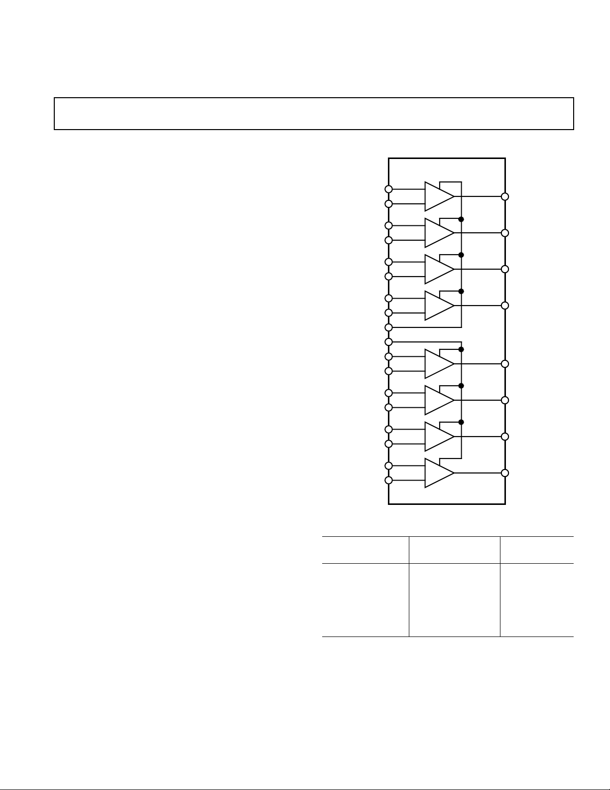
FUNCTIONAL BLOCK DIAGRAM
ADM5180
A–
B–
C–
D–
FS1
FS2
E–
F–
G–
H–
A+
B+
C+
D+
E+
F+
G+
H+
A
B
C
D
E
F
G
H
A
O
B
O
C
O
D
O
E
O
F
O
G
O
H
O
Truth Table
Differential Input Failsafe Input Receiver
(+) - (–) FS1, FS2 Logic Output
>200 mV X H
<–200 mV X L
O/C L L
S/C L L
O/C H H
S/C H H
REV. 0
Information furnished by Analog Devices is believed to be accurate and
reliable. However, no responsibility is assumed by Analog Devices for its
use, nor for any infringements of patents or other rights of third parties
which may result from its use. No license is granted by implication or
otherwise under any patent or patent rights of Analog Devices.
One Technology Way, P.O. Box 9106, Norwood. MA 02062-9106, U.S.A.
Tel: 617/329-4700 Fax: 617/326-8703
Page 2

(VDD = +5 V ± 5%, Input Common-Mode Range = ±7 V. All Specifications T
ADM5180–SPECIFICA TIONS
Parameter Min Typ Max Units Test Conditions/Comments
POWER REQUIREMENTS
V
DD
I
DD
INPUTS
Input Resistance, R
IN
Differential Input High Threshold, V
Differential Input Low Threshold, V
Hysteresis, V
Open Circuit Input Voltage, V
H
IOC
Input Capacitance 20 pF
Input Current, I
IN
OUTPUTS
High Level Output Voltage,V
Low Level Output Voltage ,V
Short Circuit O/P Current, I
OH
OL
OS
FAILSAFE FUNCTION
Failsafe Output Voltage, V
OFS
FS1, FS2 Input Current –10 +10 µA
4.75 5.25 V
37kΩ3 V ≤|VIN|≤ 25 V
50 200 mV RS = 0 Ω, V
TH
–200 –50 mV RS = 0 Ω, V
TL
–400 mV R
50 140 mV FS1, FS2 = 0 V or VDD, See Figure 1
–3.25 mA VIN = –10 V
2.7 V VID = 1.0 V, I
2.7 V 0 ≥ I
T
unless otherwise noted.)
MAX
3.5 5 mA
400 mV R
60 mV
3.25 mA VIN = +10 V
0.4 V VID = –1.0 V, I
0.45 V V
100 mA Note 1
0.40 V 0 ≤ I
0.45 V 0 ≤ I
= 500 Ω, V
S
= 500 Ω, V
S
= –1.0 V, I
ID
= 2.7 V, I
OUT
= 2.7 V, I
OUT
= 0.45 V, I
OUT
= 0.45 V, I
OUT
= –440 µA
OUT
= 4 mA
OUT
= 8 mA, TA = 0ºC to +70ºC
OUT
= –440 µA, See Figure 1
OUT
OUT
= 8 mA, See Figure 1
OUT
OUT
Inputs Open or Shorted Together or One Input Open
and One Grounded
≤ 4 mA; FS1, FS2 = 0 V
OUT
≤ 8 mA, TA = 0ºC to +70ºC; FS1, FS2 = 0 V
OUT
≥ –400 µA; FS1, FS2 = V
OUT
to
MIN
= –440 µA, See Figure 1
= 8 mA, See Figure 1
DD
NOTE
1
Only one output may be shorted at any time.
Specifications subject to change without notice.
TIMING CHARACTERISTICS
(VDD = +5 V ± 5%. All Specifications T
MIN
to T
unless otherwise noted)
MAX
Parameter Min Typ Max Units Test Conditions/Comments
Propagation Delay–Low to High 550 ns CL = 50 pF, VIN = ±500 mV
Propagation Delay–High to Low 550 ns CL = 50 pF, VIN = ±500 mV
Acceptable Input Frequency 0.1 MHz Unused Input Grounded, V
= ±200 mV
IN
Rejectable Input Frequency 5.5 MHz Unused Input Grounded, VIN = ±500 mW
Specifications subject to change without notice.
–2–
REV. 0
Page 3

ADM5180
ABSOLUTE MAXIMUM RATINGS
(TA = 25°C unless otherwise noted)
VDD . . . . . . . . . . . . . . . . . . . . . . . . . . . . . . . . . . . . . . . . . . . . +7 V
Common-Mode Input Voltage . . . . . . . . . . . . . . . . . . . . . . +15 V
Differential Input Voltage . . . . . . . . . . . . . . . . . . . . . . . . . . +25 V
Failsafe Voltage . . . . . . . . . . . . . . . . . . . . . . . . . . . . .–0.3 V to V
Output Short Circuit Duration . . . . . . . . . . . . . . . . . Continuous
Power Dissipation Plastic DIP . . . . . . . . . . . . . . . . . . . . 1250 mW
(Derate at 12.5 mW/°C Above +50°C)
, Thermal Impedance . . . . . . . . . . . . . . . . . . . . . . . . 75°C/W
θ
JA
Power Dissipation PLCC . . . . . . . . . . . . . . . . . . . . . . . 1000 mW
(Derate at 12.5 mW/°C Above +50°C)
, Thermal Impedance . . . . . . . . . . . . . . . . . . . . . . . +80°C/W
θ
JA
CAUTION
1
Operating Temperature Range
Commercial ( J Version) . . . . . . . . . . . . . . . . . . . 0°C to +70°C
Industrial (A Version) . . . . . . . . . . . . . . . . . . . –40°C to +80°C
Lead Temperature (Soldering 10 sec) . . . . . . . . . . . . . . . . +300°C
Vapour Phase (60 sec) . . . . . . . . . . . . . . . . . . . . . . . . . +215°C
CC
2
Infrared (15 sec) . . . . . . . . . . . . . . . . . . . . . . . . . . . . . . +220°C
NOTES
1
This is a stress rating only and functional operation of the device at these or any
other conditions above those indicated in the operation sections of this specification is not implied. Exposure to absolute maximum rating conditions for
extended periods of time may affect reliability.
2
Only one output should be shorted at any time.
W
ESD (electrostatic discharge) sensitive device. Electrostatic charges as high as 4000 V readily
accumulate on the human body and test equipment and can discharge without detection. Although
the ADM5180 features proprietary ESD protection circuitry, permanent damage may occur on
devices subjected to high energy electrostatic discharges. Therefore, proper ESD precautions are
recommended to avoid performance degradation or loss of functionality.
V
OUT
FS = V
DD
FS = GND
(VIN+) – (VIN–)
WARNING!
ESD SENSITIVE DEVICE
50%
V
H1
V
V
V
TH1
TL1
V
0
TL2
Figure 1. VTL, VTH, VH Definition
8mA
TO
OUTPUT
PIN
50pF
440µA
Figure 2. Timing Test Load
TH2
+2.1V
t
PLH
OUTPUT
V
H2
t
PHL
50%
Figure 3. Timing Waveform
V
IN
ORDERING GUIDE
Model Temperature Range Package Option
ADM5180JN 0°C to +70°C N-28
ADM5180AN –40°C to +85° C N-28
ADM5180JP 0°C to +70°C P-28A
ADM5180AP –40°C to +85°C P-28A
REV. 0
–3–
Page 4

ADM5180
PIN CONFIGURATIONS
DIP
1
A–
2
A+
3
A
O
4
B–
5
B+
6
B
O
ADM5180
FS1
7
TOP VIEW
8
C– FS2
(Not to Scale)
9
C+ F
10
C
O
1111
D– F–
12
D+ E
13
D
O
14
GND E–
PLCC
O
A
A+
A–
1
28423
ADM5180
TOP VIEW
(Not to Scale)
FS1
B–
5
B+
B
6
O
7
C–
8
9
C+
10
C
O
11
D–
APPLICATIONS INFORMATION
FAILSAFE OPERATION
The ADM5180 provides a failsafe operating mode to guard against
28
V
DD
27
H
O
H+
26
H–
25
G
24
O
G+
23
G–
22
21
20
O
19
F+
18
17
O
E+
16
15
O
DD
H
V
H+
26
27
25
H–
G
24
O
G+
23
G–
22
21
FS2
20
F
O
19
F+
input fault conditions as defined in RS-422A and RS-423A
standards. The fault conditions are (1) Driver in power-off
condition, (2) Receiver not interconnected with Driver, (3) Opencircuited interconnecting cable, and (4) Short-circuited interconnecting cable. If any of these four fault conditions occurs at the
inputs of a receiver, then the output of that receiver is driven to a
known logic level. The failsafe level is programmed using the
failsafe (FS) input. There are two failsafe inputs, FS1 and FS2
which each control four receivers. FSI controls receivers A ...D
and FS2 controls receivers E . . . H. A connection to V
on the
DD
failsafe input sets the output high under fault conditions while a
connection to GND sets the output low.
FS1, FS2 Output During Fault Condition
V
DD
High
GND Low
Input Filtering
The ADM5180 contains internal low pass filtering for additional
noise rejection. Frequencies above the passband will be rejected.
For the specified input (5.5 MHz at ±500 mV) the input stage
attenuates the signal such that the threshold levels are not reached
and therefore no change of state occurs on the output. The filtering
is a function of both amplitude and and frequency. As the signal
amplitude decreases then the rejected frequency will decrease.
15 18
16121413
O
D
D+
GND
17
O
E–
F–
E+
E
PIN DESCRIPTION
Mnemonic Function
V
DD
Power Supply Input, 5 V ± 5%.
GND Ground Pin. Must be connected to 0 V.
A+ . . . H+ Noninverting Input to Differential Receivers
A to H.
A– . .. H– Inverting Input to Differential Receivers A to H.
A
...H
O
Receiver Outputs A to H.
O
A through D and FS2 controls receivers
E through H.
FS1, FS2 Failsafe Control Inputs. FS1 controls receivers
A through D and FS2 control Receiver
E through H.
REV. 0–4–
Page 5

V
V
H
L
INPUT
+V
–V
1/8
ADM5170
RS232/RS423A
TRANSMISSION
Figure 4. EIA-232/V.28 Data Transmission
TIE TO GND FOR
RS232
+
1/8
ADM5180
–
V
V
DD
DD
V
V
V
FAILSAFE
ADM5180
H
L
V
OUT
+V
V
V
H
L
INPUT
RS422A/V.11
LINE DRIVER
–V
TRANSMISSION
+V
–V
Figure 5. RS-422A/V.11 Data Transmission
Typical Performance Characteristics
4.0
VDD = 5V
FS = 5V
3.8
3.6
– mA
DD
I
3.4
VID = O/C
RS422
V
H
V
V
FAILSAFE
L
V
OUT
+
–
5.5
5.3
5.1
– V
DD
V
4.9
+
–
TA = +25°C
FS = 0V
VID = O/C
1/8
ADM5180
3.2
3.0
–40
–20
TEMPERATURE – °C
6040200
Figure 6. Supply Current vs. Temperature
4.7
80
4.5
3.35
3.40
IDD – mA
3.45
3.50
Figure 7. Supply Current vs. Supply Voltage
–5–REV. 0
Page 6

ADM5180
A
0.048 (1.21)
0.042 (1.07)
0.456 (11.58)
0.450 (11.43)
SQ
0.495 (12.57)
0.485 (12.32)
SQ
0.048 (1.21)
0.042 (1.07)
0.050
(1.27)
BSC
26 4
TOP VIEW
25
19
12
11
PIN 1
IDENTIFIER
5
18
0.020
(0.50)
R
0.032 (0.81)
0.026 (0.66)
0.021 (0.53)
0.013 (0.33)
0.056 (1.42)
0.042 (1.07)
0.025 (0.63)
0.015 (0.38)
0.180 (4.57)
0.165 (4.19)
0.430 (10.92)
0.390 (9.91)
0.110 (2.79)
0.085 (2.16)
0.040 (1.01)
0.025 (0.64)
500
TpLH
400
TpHL
300
200
PROPAGATION DELAY – ns
100
0
0
1
Vpp – V (VID = ±Vpp/2)
VDD = 5V
FS = 0V
f = 100kHz
= +25°C
T
A
CL = 50pF
432
Figure 8. Propagation Delay vs. Amplitude
– V
OH
V
5.0
4.8
4.6
4.4
4.2
VDD = 5V
= +25°C
T
A
7
VDD = 5V
FS = 0V
6
= +25°C
T
A
5
4
3
2
Vpp – V (VID = ±Vpp/2)
1
0
5
0
1
REJECTABLE INPUT FREQUENCY – MHz
2
3
4
C1854–7.5–10/93
Figure 10. Rejectable Input Frequency vs. Amplitude
1000
VDD = 5V
FS = 0V
VID = 1V
800
600
– mV
OL
V
400
T
A
A
= +25°C
4.0
3.8
0
1
IOH – mA
432
Figure 9. High Level Output Voltage vs. Output
Source Current
28-Lead Plastic DIP
(N Suffix)
0.070 (1.77)
MAX
0.195 (4.95)
0.125 (3.18)
15
0.580 (14.73)
0.485 (12.32)
14
0.060 (1.52)
0.015 (0.38)
SEATING
PLANE
PIN 1
0.250
(6.35)
MAX
0.200 (5.05)
0.125 (3.18)
28
1
0.022 (0.558)
0.014 (0.356)
1.565 (39.70)
1.380 (35.10)
0.100
(2.54)
BSC
0.625 (15.87)
0.600 (15.24)
0.015 (0.381)
0.008 (0.204)
200
5
0
0
Figure 11. Low Level Output Voltage vs. Output
Sink Current
OUTLINE DIMENSIONS
Dimensions shown in inches and (mm).
28-Lead Plastic Leaded Chip Carrier (PLCC)
0.150
(3.81)
MIN
–6–
10
IOL – mA
(P Suffix)
20
30
PRINTED IN U.S.A.
REV. 0
 Loading...