

Page 1
www.BDTIC.com/ADI
5 V Slew-Rate Limited Half- and Full-Duplex
FEATURES
EIA RS-485-/RS-422-compliant
Data rate options
ADM4850/ADM4854—115 kbps
ADM4851/ADM4855—500 kbps
ADM4852/ADM4856—2.5 Mbps
ADM4853/ADM4857—10 Mbps
Half- and full-duplex options
Reduced slew rates for low EMI
True fail-safe receiver inputs
5 µA (maximum) supply current in shutdown mode
Up to 256 transceivers on one bus
Outputs high-z when disabled or powered off
−7 V to +12 V bus common-mode range
Thermal shutdown and short-circuit protection
Pin-compatible with MAX308x
Specified over the −40°C to +85°C temperature range
Available in 8-lead SOIC and LFCSP packages
APPLICATIONS
Low power RS-485 applications
EMI-sensitive systems
DTE-DCE interfaces
Industrial control
Packet switching
Local area networks
Level translators
RS-485/RS-422 Transceivers
ADM4850–ADM4857
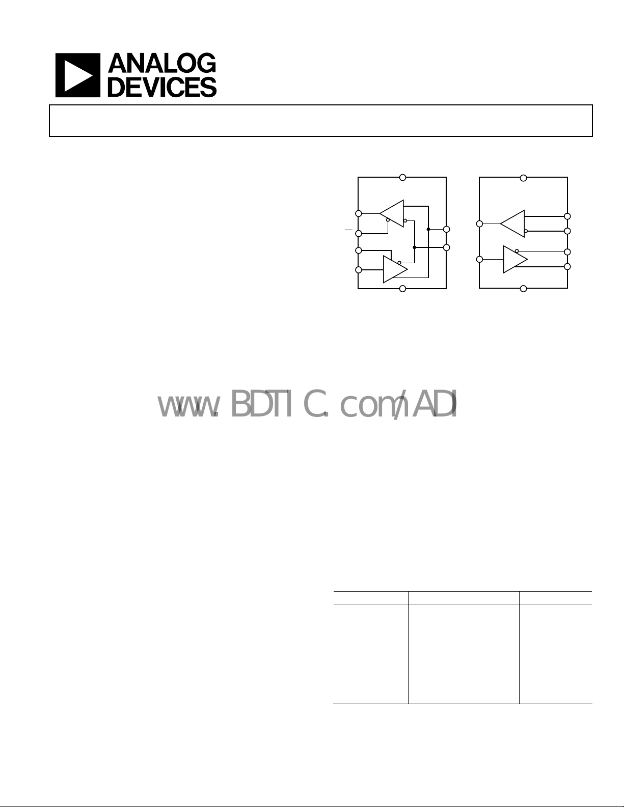
FUNCTIONAL BLOCK DIAGRAM
ADM4850/ADM4851/
ADM4852/ADM4853
RO
RE
DE
DI
V
CC
ADM4854/ADM4855/
ADM4856/ADM4857
R
D
GND
RO
A
B
DI
Figure 1.
V
CC
R
D
GND
A
B
Z
Y
04931-001
GENERAL DESCRIPTION
The ADM4850−ADM4857 are differential line transceivers
suitable for high speed half- and full-duplex data communication
on multipoint bus transmission lines. They are designed for
balanced data transmission and comply with EIA Standards
RS-485 and RS-422. The ADM4850−ADM4853 are half-duplex
transceivers, which share differential lines and have separate
enable inputs for the driver and receiver. The full-duplex
ADM4854−ADM4857 transceivers have dedicated differential
line driver outputs and receiver inputs.
The parts have a 1/8-unit-load receiver input impedance, which
allows up to 256 transceivers on one bus. Since only one driver
should be enabled at any time, the output of a disabled or powered-down driver is three-stated to avoid overloading the bus.
The receiver inputs have a true fail-safe feature, which ensures a
logic high output level when the inputs are open or shorted.
This guarantees that the receiver outputs are in a known state
before communication begins and when communication ends.
Rev. 0
Information furnished by Analog Devices is believed to be accurate and reliable.
However, no responsibility is assumed by Analog Devices for its use, nor for any
infringements of patents or other rights of third parties that may result from its use.
Specifications subject to change without notice. No license is granted by implication
or otherwise under any patent or patent rights of Analog Devices. Trademarks and
registered trademarks are the property of their respective owners.
The driver outputs are slew-rate limited to reduce EMI and data
errors caused by reflections from improperly terminated buses.
Excessive power dissipation caused by bus contention or by
output shorting is prevented with a thermal shutdown circuit.
The parts are fully specified over the commercial and industrial
temperature ranges, and are available in 8-lead SOIC and LFCSP
packages.
Table 1. Selection Table
Part No Half-/Full-Duplex Data Rate
ADM4850 Half 115 kbps
ADM4851 Half 500 kbps
ADM4852 Half 2.5 Mbps
ADM4853 Half 10 Mbps
ADM4854 Full 115 kbp
ADM4855 Full 500 kbps
ADM4856 Full 2.5 Mbps
ADM4857 Full 10 Mbps
One Technology Way, P.O. Box 9106, Norwood, MA 02062-9106, U.S.A.
Tel: 781.329.4700 www.analog.com
Fax: 781.326.8703 © 2004 Analog Devices, Inc. All rights reserved.
Page 2

ADM4850–ADM4857
www.BDTIC.com/ADI
TABLE OF CONTENTS
Specifications..................................................................................... 3
Circuit Description......................................................................... 12
ADM4850/ADM4854 Timing Specifications........................... 4
ADM4851/ADM4855 Timing Specifications........................... 4
ADM4852/ADM4856 Timing Specifications........................... 5
ADM4853/ADM4857 Timing Specifications........................... 5
Absolute Maximum Ratings............................................................ 6
ESD Caution.................................................................................. 6
Pin Configurations and Function Descriptions ........................... 7
Test Ci r c ui t s ....................................................................................... 8
Switching Characteristics ................................................................ 9
Typical Performance Characteristics ........................................... 10
REVISION HISTORY
10/04—Revision 0: Initial Version
Slew-Rate Control ...................................................................... 12
Receiver Input Filtering............................................................. 12
Half-/Full-Duplex Operation ................................................... 12
High Receiver Input Impedance .............................................. 13
Three-State Bus Connection..................................................... 13
Shutdown Mode ......................................................................... 13
Fail-Safe Operation .................................................................... 13
Current Limit and Thermal Shutdown ................................... 13
Outline Dimensions ....................................................................... 14
Ordering Guide .......................................................................... 15
Rev. 0 | Page 2 of 16
Page 3
ADM4850–ADM4857
www.BDTIC.com/ADI
SPECIFICATIONS
V = 5 V ± 5%, TA = T
Table 2.
Parameter Min Typ Max Unit Test Conditions/Comments
DRIVER
Differential Output Voltage, V
2.0 5 V R = 50 Ω (RS-422), Figure 4
1.5 5 V R = 27 Ω (RS-485), Figure 4
1.5 5 V V
∆|VOD| for Complementary Output States 0.2 V R = 27 Ω or 50 Ω, Figure 4
Common-Mode Output Voltage, VO 3 V R = 27 Ω or 50 Ω, Figure 4
∆|VO | for Complementary Output States 0.2 V R = 27 Ω or 50 Ω, Figure 4
Output Short-Circuit Current, V
Output Short-Circuit Current, V
DRIVER INPUT LOGIC
CMOS Input Logic Threshold Low 1.4 0.8 V
CMOS Input Logic Threshold High 2.0 1.4 V
CMOS Logic Input Current (DI) ±1 µA
DE Input Resistance to GND 220 kΩ
RECEIVER
Differential Input Threshold Voltage, V
Input Hysteresis 20 mV −7 V < VM < +12 V
Input Resistance (A, B) 96 150 kΩ −7 V < VM < +12 V
Input Current (A, B) 0.125 mA VIN = +12 V
−0.1 mA V
CMOS Logic Input Current (RE)
CMOS Output Voltage Low 0.4 V I
CMOS Output Voltage High 4.0 V I
Output Short Circuit Current 7 85 mA V
Three-State Output Leakage Current ±2 µA 0.4 V ≤ V
POWER SUPPLY CURRENT
I (115 kbps Options) 5 µA
36 60 µA
100 160 µA DE = VCC
I (500 kbps Options) 5 µA
80 120 µA
120 200 µA DE = V
I (2.5 Mbps Options) 5 µA
250 400 µA
320 500 µA DE = VCC
I (10 Mbps Options) 5 µA
250 400 µA
320 500 µA DE = VCC
1
Guaranteed by design.
MIN
to T
, unless otherwise noted.
MAX
OD
= High −200 +200 mA −7 V < V
OUT
= Low −200 +200 mA −7 V < V
OUT
TH
VCCV
−200 −125 −30 mV −7 V < VM < +12 V
±1 µA
R = ∞, Figure 4
= −7 V to 12 V, Figure 5
TST
= −7 V
IN
= +4 mA
OUT
= −4 mA
OUT
= GND or V
OUT
DE = 0 V, RE
DE = 0 V, RE
DE = 0 V, RE
DE = 0 V, RE
CC
DE = 0 V, RE
DE = 0 V, RE
DE = 0 V, RE
DE = 0 V, RE
1
< +12 V
OUT
< +12 V
OUT
CC
≤ 2.4 V
OUT
= VCC (shutdown)
= 0 V
= VCC (shutdown)
= 0 V
= VCC (shutdown)
= 0 V
= VCC (shutdown)
= 0 V
Rev. 0 | Page 3 of 16
Page 4
ADM4850–ADM4857
www.BDTIC.com/ADI
ADM4850/ADM4854 TIMING SPECIFICATIONS
V = 5 V ± 5%, TA = T
Table 3.
Parameter Min Typ Max Unit Test Conditions/Comments
DRIVER
Maximum Data Rate 115 kbps
Propagation Delay t
Skew t
SKEW
Rise/Fall Time tR, t
Enable Time 2000 ns RL = 500 Ω, CL = 100 pF, Figure 7, ADM4850
Disable Time 2000 ns RL = 500 Ω, CL = 15 pF, Figure 7, ADM4850
Enable Time from Shutdown 4000 ns RL = 500 Ω, CL = 100 pF, Figure 7, ADM4850
RECEIVER
Propagation Delay t
Differential Skew t
Enable Time 5 50 ns RL = 1 kΩ, CL = 15 pF, Figure 9, ADM4850
Disable Time 20 50 ns RL = 1 kΩ, CL = 15 pF, Figure 9, ADM4850
Enable Time from Shutdown 4000 ns RL = 1 kΩ, CL = 15 pF, Figure 9, ADM4850
Time to Shut Down 50 330 3000 ns ADM4850
1
The half-duplex device is put into shutdown mode by driving RE high and DE low. If these inputs are in this state for less than 50 ns, the device is guaranteed not to
enter shutdown mode. If the enable inputs are in this state for at least 3000 ns, the device is guaranteed to enter shutdown mode.
ADM4851/ADM4855 TIMING SPECIFICATIONS
F
SKEW
MIN
PLH
PLH
to T
, t
PHL
, t
PH
, unless otherwise noted.
MAX
600 2500 ns R
70 ns R
600 2400 ns R
400 1000 ns CL = 15 pF, Figure 8
255 ns CL = 15 pF, Figure 8
= 54 Ω, CL1 = CL2 = 100 pF, Figure 6
LDIFF
= 54 Ω, CL1 = CL2 = 100 pF, Figure 6
LDIFF
= 54 Ω, C
LDIFF
= CL2 = 100 pF, Figure 6
L1
1
V = 5 V ± 5%, TA = T
MIN
to T
, unless otherwise noted.
MAX
Table 4.
Parameter Min Typ Max Unit Test Conditions/Comments
DRIVER
Maximum Data Rate 500 kbps
Propagation Delay t
Skew t
SKEW
Rise/Fall Time tR, t
, t
PLH
PHL
F
250 600 ns R
40 ns R
200 600 ns R
= 54 Ω, CL1 = CL2 = 100 pF, Figure 6
LDIFF
= 54 Ω, CL1 = CL2 = 100 pF, Figure 6
LDIFF
= 54 Ω, CL1 = C
LDIFF
= 100 pF, Figure 6
L2
Enable Time 1000 ns RL = 500 Ω, CL = 100 pF, Figure 7, ADM4851
Disable Time 1000 ns RL = 500 Ω, CL = 15 pF, Figure 7, ADM4851
Enable Time from Shutdown 4000 ns RL = 500 Ω, CL = 100 pF, Figure 7, ADM4851
RECEIVER
Propagation Delay t
Differential Skew t
SKEW
PLH
, t
PHL
400 1000 ns CL = 15 pF, Figure 8
250 ns CL = 15 pF, Figure 8
Enable Time 5 50 ns RL = 1 kΩ, CL = 15 pF, Figure 9, ADM4851
Disable Time 20 50 ns RL =1 kΩ, CL = 15 pF, Figure 9, ADM4851
Enable Time from Shutdown 4000 ns RL =1 kΩ, CL = 15 pF, Figure 9, ADM4851
Time to Shut Down 50 330 3000 ns ADM4851
1
1
The half-duplex device is put into shutdown mode by driving RE high and DE low. If these inputs are in this state for less than 50 ns, the device is guaranteed not to
enter shutdown mode. If the enable inputs are in this state for at least 3000 ns, the device is guaranteed to enter shutdown mode.
Rev. 0 | Page 4 of 16
Page 5
ADM4850–ADM4857
www.BDTIC.com/ADI
ADM4852/ADM4856 TIMING SPECIFICATIONS
V = 5 V ± 5%, TA = T
Table 5.
Parameter Min Typ Max Unit Test Conditions/Comments
DRIVER
Maximum Data Rate 2.5 Mbps
Propagation Delay t
Skew t
SKEW
Rise/Fall Time tR, t
Enable Time 180 ns RL = 500 Ω, CL = 100 pF, Figure 7, ADM4852
Disable Time 180 ns RL = 500 Ω, CL = 15 pF, Figure 7, ADM4852
Enable Time from Shutdown 4000 ns RL =500 Ω, CL = 100 pF, Figure 7, ADM4852
RECEIVER
Propagation Delay t
Differential Skew t
Enable Time 5 50 ns RL = 1 kΩ, CL = 15 pF, Figure 9, ADM4852
Disable Time 20 50 ns RL = 1 kΩ, CL = 15 pF, Figure 9, ADM4852
Enable Time from Shutdown 4000 ns RL = 1 kΩ, CL = 15 pF, Figure 9, ADM4852
Time to Shut Down 50 330 3000 ns ADM4852
1
The half-duplex device is put into shutdown mode by driving RE high and DE low. If these inputs are in this state for less than 50 ns, the device is guaranteed not to
enter shutdown mode. If the enable inputs are in this state for at least 3000 ns, the device is guaranteed to enter shutdown mode.
ADM4853/ADM4857 TIMING SPECIFICATIONS
V = 5 V ± 5%, TA = T
Table 6.
Parameter Min Typ Max Unit Test Conditions/Comments
DRIVER
Maximum Data Rate 10 Mbps
Propagation Delay t
Skew t
SKEW
Rise/Fall Time tR, t
Enable Time 35 ns RL = 500 Ω, CL = 100 pF, Figure 7, ADM4853
Disable Time 35 ns RL = 500 Ω, CL = 15 pF, Figure 7, ADM4853
Enable Time from Shutdown 4000 ns RL = 500 Ω, CL = 100 pF, Figure 7, ADM4853
RECEIVER
Propagation Delay t
Differential Skew t
Enable Time 5 50 ns RL = 1 kΩ, CL = 15 pF, Figure 9, ADM4853
Disable Time 20 50 ns RL = 1 kΩ, CL = 15 pF, Figure 9, ADM4853
Enable Time from Shutdown 4000 ns RL = 1 kΩ, CL = 15 pF, Figure 9, ADM4853
Time to Shut Down 50 330 3000 ns ADM48531
1
The half-duplex device is put into shutdown mode by driving RE high and DE low. If these inputs are in this state for less than 50 ns, the device is guaranteed not to
enter shutdown mode. If the enable inputs are in this state for at least 3000 ns, the device is guaranteed to enter shutdown mode.
F
SKEW
F
SKEW
MIN
PLH
PLH
MIN
PLH
PLH
to T
, t
PHL
, t
PHL
to T
, t
PHL
, t
PHL
, unless otherwise noted.
MAX
50 180 ns R
50 ns R
140 ns R
55 190 ns CL = 15 pF, Figure 8
50 ns CL = 15 pF, Figure 8
, unless otherwise noted.
MAX
0 30 ns R
10 ns R
30 ns R
55 190 ns CL = 15 pF, Figure 8
30 ns CL = 15 pF, Figure 8
= 54 Ω, CL1 = CL2 = 100 pF, Figure 6
LDIFF
= 54 Ω, CL1 = CL2 = 100 pF, Figure 6
LDIFF
= 54 Ω, CL1 = CL2 = 100 pF, Figure 6
LDIFF
1
= 54 Ω, CL1 = CL2 = 100 pF, Figure 6
LDIFF
= 54 Ω, CL1 = CL2 = 100 pF, Figure 6
LDIFF
= 54 Ω, CL1 = CL2 = 100 pF, Figure 6
LDIFF
Rev. 0 | Page 5 of 16
Page 6

ADM4850–ADM4857
www.BDTIC.com/ADI
ABSOLUTE MAXIMUM RATINGS
Table 7.
Parameter Rating
VCC to GND 6 V
Digital I/O Voltage (DE, RE, DI, ROUT) −0.3 V to VCC + 0.3 V
Driver Output/Receiver Input Voltage −9 V to +14 V
Operating Temperature Range −40°C to +85°C
Storage Temperature Range −65°C to +125°C
θJA Thermal Impedance
SOIC 110°C/W
LFCSP 62°C/W
Lead Temperature
Soldering (10 s) 300°C
Vapour Phase (60 s) 215°C
Infrared (15 s) 220°C
Stresses above those listed under Absolute Maximum Ratings
may cause permanent damage to the device. This is a stress
rating only; functional operation of the device at these or any
other conditions above those indicated in the operational
section of this specification is not implied. Exposure to absolute
maximum rating conditions for extended periods may affect
device reliability.
ESD CAUTION
ESD (electrostatic discharge) sensitive device. Electrostatic charges as high as 4000 V readily accumulate on
the human body and test equipment and can discharge without detection. Although this product features
proprietary ESD protection circuitry, permanent damage may occur on devices subjected to high energy
electrostatic discharges. Therefore, proper ESD precautions are recommended to avoid performance
degradation or loss of functionality.
Rev. 0 | Page 6 of 16
Page 7

ADM4850–ADM4857
www.BDTIC.com/ADI
PIN CONFIGURATIONS AND FUNCTION DESCRIPTIONS
RO
RE
DE
DI
1
ADM4850/
ADM4851/
2
ADM4852/
ADM4853
TOP VIEW
4
(Not to Scale)
8
V
CC
B
7
A
63
GND
5
04931-002
Figure 2. ADM4850–ADM4853 Pin Configuration
Table 8. ADM4850–ADM4853 Pin Descriptions
Pin No. Mnemonic Description
1 RO
Receiver Output. When enabled, if (A−B) ≥ −30 mV, then RO = high.
If (A−B) ≤ −200 mV, then RO = low.
2
RE
Receiver Output Enable.
A low level enables the receiver output, RO.
A high level places it in a high impedance state.
3 DE
Driver Output Enable. A high level enables the driver differential inputs A and B.
A low level places it in a high impedance state.
4 DI
Driver Input. When the driver is enabled, a logic low on DI forces A low and B high,
while a logic high on DI forces A high and B low.
5 GND Ground.
6 A Noninverting Receiver Input A/Driver Output A.
7 B Inverting Receiver Input B/Driver Output B.
8 VCC 5 V Power Supply.
A
V
RO
GND
CC
DI
1
ADM4854/
ADM4855/
2
ADM4856/
ADM4857
TOP VIEW
4
(Not to Scale)
8
B
7
Z
63
Y
5
Figure 3. ADM4854–ADM4857 Pin Configuration
Table 9. ADM4854–ADM4857 Pin Descriptions
Pin No. Mnemonic Description
1 VCC 5 V Power Supply.
2 RO
Receiver Output. When enabled, if (A−B) ≥ −30 mV, then RO = high.
If (A−B) ≤ −200 mV, then RO = low.
3 DI
Driver Input. When the driver is enabled, a logic low on DI forces Y low and Z high,
while a logic high on DI forces Y high and Z low.
4 GND Ground.
5 Y Driver Noninverting Output.
6 Z Driver Inverting Output.
7 B Receiver Inverting Input.
8 A Receiver Noninverting Input.
04931-003
Rev. 0 | Page 7 of 16
Page 8

ADM4850–ADM4857
www.BDTIC.com/ADI
TEST CIRCUITS
Figure 4. Driver Voltage Measurement
V
375Ω
V
R
OD
R
V
OC
04931-004
0V OR 3V
DE IN
DE
A
S1
C
B
V
L
Figure 7. Driver Enable/Disable
R
OUT
CC
L
S2
04931-007
V
V
OD3
60Ω
375Ω
TST
04931-005
Figure 5. Driver Voltage Measurement over Common-Mode Voltage Range
A
R
LDIFF
B
C
L1
C
L2
04931-006
Figure 6. Driver Propagation Delay
A
V
RE
B
OUT
C
L
04931-008
Figure 8. Receiver Propagation Delay
+1.5V
–1.5V
RE IN
S1
RE
C
L
V
CC
R
L
S2
V
OUT
04931-009
Figure 9. Receiver Enable/Disable
Rev. 0 | Page 8 of 16
Page 9

ADM4850–ADM4857
3V0V5V0
www.BDTIC.com/ADI
SWITCHING CHARACTERISTICS
3V
DE
A, B
A, B
1.5V
t
ZL
t
ZH
2.3V
2.3V
1.5V
t
LZ
t
HZ
0V
V
+0.5V
OL
V
OH
–0.5V
V
OL
V
OH
0V
04931-012
Figure 12. Driver Enable/Disable Timing
3V
RE
1.5V
t
ZL
1.5V
t
LZ
0V
1.5V
t
PLH
B
1/2VO
VO
A
10% POINT
V
90% POINT
t
R
t
SKEW
=
|t
PLH –tPHL
Figure 10. Driver Propagation Delay, Rise/Fall Timing
0VA, B
1.5V
t
PHL
|
90% POINT
10% POINT
t
F
0V
04931-010
1.5V
O/P LOW
t
ZH
O/P HIGH
1.5V
V
+0.5V
OL
t
HZ
–0.5V
V
OH
Figure 13. Receiver Enable/Disable Timing
V
OL
V
OH
04931-013
RO
t
PLH
1.5V 1.5V
t
=
|t
SKEW
PLH –tPHL
t
|
Figure 11. Receiver Propagation Delay
PHL
R
V
OH
R
V
OL
04931-011
0V
Rev. 0 | Page 9 of 16
Page 10

ADM4850–ADM4857
www.BDTIC.com/ADI
TYPICAL PERFORMANCE CHARACTERISTICS
400
350
300
250
200
150
ADM4853: DE = V
ADM4853: DE = GND
ADM4850: DE = V
CC
CC
0.40
0.35
0.30
0.25
100
UNLOADED SUPPLY CURRENT (µA)
50
0
–50 –25 0 25 50 75 100 125
TEMPERATURE (°C)
ADM4850: DE = GND
Figure 14. Unloaded Supply Current vs. Temperature
50
45
40
35
30
25
20
15
10
RECEIVER OUTPUT CURRENT (mA)
5
0
0 0.2 0.4 0.6 0.8 1.0 1.2 1.4 1.6 1.8 2.0
RECEIVER OUTPUT LOW VOLTAGE (V)
Figure 15. Output Current vs. Receiver Output Low Voltage
5
0
–5
–10
–15
RECEIVER OUTPUT CURRENT (mA)
–20
3.5 4.0 4.5 5.0 5.5
Figure 16. Output Current vs. Receiver Output High Voltage
RECEIVER OUTPUT HIGH VOLTAGE (V)
04931-014
04931-015
04931-016
OUTPUT LOW VOLTAGE (V)
0.20
0.15
–50 –25 0 25 50 75 100 125
TEMPERATURE (
°
C)
Figure 17. Receiver Output Low Voltage vs. Temperature
4.6
4.5
4.4
4.3
4.2
OUTPUT HIGH VOLTAGE (V)
4.1
4.0
–50–250 255075100125
TEMPERATURE (
°
C)
Figure 18. Receiver Output High Voltage Temperature
90
80
70
60
50
40
30
20
DRIVER OUTPUT CURRENT (mA)
10
0
0 0.5 1.0 1.5 2.0 2.5 3.0 3.5 4.0 4.5 5.0
Figure 19. Driver Output Current vs. Differential Output Voltage
DIFFERENTIAL OUTPUT VOLTAGE (V)
04931-017
04931-018
04931-019
Rev. 0 | Page 10 of 16
Page 11

ADM4850–ADM4857
www.BDTIC.com/ADI
120
100
80
60
40
OUTPUT CURRENT (mA)
20
0
0 0.5 1.0 1.5 2.0 2.5 3.0 3.5 4.0 4.5 5.0
OUTPUT VOLTAGE (V)
04931-020
Figure 20. Output Current vs. Driver Low Voltage
–10
–30
–50
800
700
600
500
400
300
200
PROPAGATION DELAY (ns)
100
0
–50 –25 0 25 50 75 100 125
ADM4855
ADM4853
TEMPERATURE (°C)
04931-023
Figure 23. Receiver Propagation Delay vs. Temperature
3
–70
OUTPUT CURRENT (mA)
–90
–110
0 0.5 1.0 1.5 2.0 2.5 3.0 3.5 4.0 4.5 5.0
OUTPUT VOLTAGE (V)
04931-021
Figure 21. Output Current vs. Driver Output High Voltage
450
400
350
300
250
200
150
PROPAGATION DELAY (ns)
100
50
0
–50 –25 0 25 50 75 100 125
TEMPERATURE (°C)
Figure 22. Driver Propagation Delay vs. Temperature
ADM4855
ADM4853
04931-022
2
4
CH1 1.00VΩ
CH3 2.00VΩ
B
W
B
W
CH2 1.00VΩ
CH4 5.00VΩ
B
W
M400ns CH3 2.00V
Figure 24. Driver/Receiver Propagation Delay (ADM4855, 500 kbps)
1
2
4
CH1 2.00VΩ
CH3 1.00VΩ
Figure 25. Driver/ Receiver Propagation Delay (ADM4855, 4 Mbps)
B
CH2 1.00VΩ M 50.0ns CH1 480mV
W
B
CH4 5.00VΩ
W
04931-024
04931-025
Rev. 0 | Page 11 of 16
Page 12

ADM4850–ADM4857
www.BDTIC.com/ADI
CIRCUIT DESCRIPTION
The ADM4850–ADM4857 are high speed RS-485/RS-422
transceivers offering enhanced performance over industrystandard devices. All devices in the family contain one driver
and one receiver, but offer a choice of performance options. The
devices feature true fail-safe operation, which means that a logic
high receiver output is guaranteed when the receiver inputs are
open-circuit or short-circuit, or when they are connected to a
terminated transmission line with all drivers disabled (see the
Fail-Safe Operation section).
SLEW-RATE CONTROL
The ADM4850/ADM4854 feature a controlled slew-rate driver
that minimizes electromagnetic interference (EMI) and reduces
reflections caused by incorrectly terminated cables, allowing
error-free data transmission rates up to 115 kbps. The ADM4851/
ADM4855 offer a higher limit on driver output slew rate, allowing
data transmission rates up to 500 kbps. The driver slew rates of
the ADM4852/ADM4856 and the ADM4853/ADM4857 are not
limited, offering data transmission rates up to 2.5 Mbps and
10 Mbps, respectively.
RECEIVER INPUT FILTERING
The receivers of all the devices incorporate input hysteresis. In
addition, the receivers of the 115 kbps ADM4850/ADM485 and
the 500 kbps ADM4851/ADM4855 incorporate input filtering.
This enhances noise immunity with differential signals that have
very slow rise and fall times. However, it causes the propagation
delay to increase by 20%.
HALF-/FULL-DUPLEX OPERATION
Half-duplex operation implies that the transceiver can transmit
and receive, but it can only do one of these at any given time.
However, with full-duplex operation, the transceiver can
transmit and receive simultaneously. The ADM4850–ADM4853
are half-duplex devices in which the driver and receiver share
differential bus terminals. The ADM4854–ADM4857 are fullduplex devices, which have dedicated driver output and receiver
input pins. Figure 26
duplex topologies.
and Figure 27 show typical half- and full-
ADM4850/ADM4851/
ADM4852/ADM4853
RO
RE
DE
DI
D
RO
R
ADM4854/ADM4855/
ADM4856/ADM4857
DI
V
DD
D
GND
A
B
AB
R
ADM4852/ADM4853
ADM4850/ADM4851/
RO RE DE DI
MAXIMUM NUMBER OF TRANSCEIVERS ON BUS: 256
Figure 26. Typical Half-Duplex RS-485 Network Topology
R
Figure 27. Typical Full-Duplex Point-to-Point RS-485 Network Topology
D
ADM4850/ADM4851/
A
B
Z
Y
AB
R
ADM4852/ADM4853
RO RE DE DI
D
ADM4854/ADM4855/
ADM4856/ADM4857
Z
Y
A
B
ADM4850/ADM4851/
ADM4852/ADM4853
A
B
V
DD
D
R
GND
DI
RO
R
D
04931-027
RO
RE
DE
DI
04931-026
Rev. 0 | Page 12 of 16
Page 13

ADM4850–ADM4857
www.BDTIC.com/ADI
HIGH RECEIVER INPUT IMPEDANCE
The input impedance of the ADM485x receivers is 96 kΩ,
which is 8 times higher than the standard RS-485 unit load of
12 kΩ. This 96 kΩ impedance, enables a standard driver to
drive 32 unit loads or be connected to 256 ADM485x receivers.
An RS-485 bus, driven by a single standard driver, can be
connected to a combination of ADM485x and standard unit
load receivers, up to an equivalent of 32 standard unit loads.
THREE-STATE BUS CONNECTION
The half-duplex parts have a driver enable (DE) pin that enables
the driver outputs when taken high, or puts the driver outputs
into a high impedance state when taken low. Similarly, the halfduplex devices have an active-low receiver enable (
Taking this pin low enables the receiver, while taking it high
puts the receiver outputs into a high impedance state. This
allows several driver outputs to be connected to an RS-485 bus.
Note that only one driver should be enabled at a time, while
many receivers can be enabled.
RE
) pin.
SHUTDOWN MODE
The ADM4850–ADM4853 have a low power shutdown mode,
which is enabled by taking
mode is not used, the fact that DE is active high and
low offers a convenient way of switching the device between
transmit and receive by tying DE and
high and DE low. If shutdown
RE
RE
together.
RE
is active
FAIL-SAFE OPERATION
The ADM4850–ADM4857 offer true fail-safe operation while
remaining fully compliant with the ±200 mV EIA/TIA-485
standard. A logic-high receiver output is generated when the
receiver inputs are shorted together or open-circuit, or when
they are connected to a terminated transmission line with all
drivers disabled. This is done by setting the receiver threshold
between −30 mV and −200 mV. If the differential receiver input
voltage (A-B) is greater than or equal to −30 mV, RO is logic
high. If A-B is less than or equal to −200 mV, RO is logic low. In
the case of a terminated bus with all transmitters disabled, the
receiver’s differential input voltage is pulled to 0 V by the
ADM485x’s internal circuitry, which results in a logic high with
30 mV minimum noise margin.
CURRENT LIMIT AND THERMAL SHUTDOWN
The ADM485x incorporates two protection mechanisms to
guard the drivers against short circuits, bus contention, or other
fault conditions. The first is a current-limiting output stage,
which protects the driver against short circuits over the entire
common-mode voltage range by limiting the output current to
approximately 70 mA. Under extreme fault conditions where
the current limit is not effective, a thermal shutdown circuit
puts the driver outputs into a high impedance state if the die
temperature exceeds 150°C, and does not turn them back on
until the temperature falls to 130°C.
The devices are guaranteed not to enter shutdown mode if DE
a
nd
are driven in this way. If DE is low and RE is high for
RE
less than 50 ns, the device does not enter shutdown mode. If DE
is low and
guaranteed to enter shutdown mode.
is high for less than 3000 ns, the device is
RE
Rev. 0 | Page 13 of 16
Page 14

ADM4850–ADM4857
www.BDTIC.com/ADI
OUTLINE DIMENSIONS
5.00 (0.1968)
4.80 (0.1890)
4.00 (0.1574)
3.80 (0.1497)
0.25 (0.0098)
0.10 (0.0040)
COPLANARITY
0.10
CONTROLLING DIMENSIONS ARE IN MILLIMETERS; INCH DIMENSIONS
(IN PARENTHESES) ARE ROUNDED-OFF MILLIMETER EQUIVALENTS FOR
REFERENCE ONLY AND ARE NOT APPROPRIATE FOR USE IN DESIGN
85
1.27 (0.0500)
SEATING
PLANE
COMPLIANT TO JEDEC STANDARDS MS-012AA
Figure 28. 8-Lead Standard Small Outline Package [SOIC]
Dimensions shown in millimeters and (inches)
6.20 (0.2440)
5.80 (0.2284)
41
BSC
0.51 (0.0201)
0.31 (0.0122)
Narrow Body (R-8)
1.75 (0.0688)
1.35 (0.0532)
0.25 (0.0098)
0.17 (0.0067)
8°
0°
0.50 (0.0196)
0.25 (0.0099)
1.27 (0.0500)
0.40 (0.0157)
× 45°
0.50
0.40
EXPOSED
PAD
(BOTTOMVIEW)
4
0.30
1
1.60
1.45
1.30
1.50
REF
PIN 1
INDICATOR
1.90
1.75
1.60
3.00
BSC SQ
PIN 1
INDICATOR
0.90
0.85
0.80
SEATING
PLANE
12° MAX
0.30
0.23
0.18
TOP
VIEW
0.80 MAX
0.65TYP
2.75
BSC SQ
0.20 REF
0.05 MAX
0.02 NOM
0.45
0.50
BSC
0.60 MAX
0.25
MIN
8
5
Figure 29. 8-Lead Lead Frame Chip Scale Package [LFCSP]
(CP-8-2)
Dimensions shown in millimeters
Rev. 0 | Page 14 of 16
Page 15

ADM4850–ADM4857
www.BDTIC.com/ADI
ORDERING GUIDE
Model Temperature Range Package Description Package Type Branding
ADM4850ACP-REEL −40°C to +85°C 8-Lead Lead Frame Chip Scale Package CP-8-2 M0R
ADM4850ACP-REEL7 −40°C to +85°C 8-Lead Lead Frame Chip Scale Package CP-8-2 M0R
ADM4850AR −40°C to +85°C 8-Lead Standard Small Outline Package R-8
ADM4850AR-REEL −40°C to +85°C 8-Lead Standard Small Outline Package R-8
ADM4850AR-REEL7 −40°C to +85°C 8-Lead Standard Small Outline Package R-8
ADM4851ACP-REEL −40°C to +85°C 8-Lead Lead Frame Chip Scale Package CP-8-2 M0S
ADM4851ACP-REEL7 −40°C to +85°C 8-Lead Lead Frame Chip Scale Package CP-8-2 M0S
ADM4851AR −40°C to +85°C 8-Lead Standard Small Outline Package R-8
ADM4851AR-REEL −40°C to +85°C 8-Lead Standard Small Outline Package R-8
ADM4851AR-REEL7 −40°C to +85°C 8-Lead Standard Small Outline Package R-8
ADM4852ACP-REEL −40°C to +85°C 8-Lead Lead Frame Chip Scale Package CP-8-2 M0T
ADM4852ACP-REEL7 −40°C to +85°C 8-Lead Lead Frame Chip Scale Package CP-8-2 M0T
ADM4852AR −40°C to +85°C 8-Lead Standard Small Outline Package R-8
ADM4852AR-REEL −40°C to +85°C 8-Lead Standard Small Outline Package R-8
ADM4852AR-REEL7 −40°C to +85°C 8-Lead Standard Small Outline Package R-8
ADM4853ACP-REEL −40°C to +85°C 8-Lead Lead Frame Chip Scale Package CP-8-2 M0U
ADM4853ACP-REEL7 −40°C to +85°C 8-Lead Lead Frame Chip Scale Package CP-8-2 M0U
ADM4853AR −40°C to +85°C 8-Lead Standard Small Outline Package R-8
ADM4853AR-REEL −40°C to +85°C 8-Lead Standard Small Outline Package R-8
ADM4853AR-REEL7 −40°C to +85°C 8-Lead Standard Small Outline Package R-8
ADM4854AR −40°C to +85°C 8-Lead Standard Small Outline Package R-8
ADM4855AR −40°C to +85°C 8-Lead Standard Small Outline Package R-8
ADM4855AR-REEL −40°C to +85°C 8-Lead Standard Small Outline Package R-8
ADM4855AR-REEL7 −40°C to +85°C 8-Lead Standard Small Outline Package R-8
ADM4856AR −40°C to +85°C 8-Lead Standard Small Outline Package R-8
ADM4856AR-REEL −40°C to +85°C 8-Lead Standard Small Outline Package R-8
ADM4856AR-REEL7 −40°C to +85°C 8-Lead Standard Small Outline Package R-8
ADM4857AR −40°C to +85°C 8-Lead Standard Small Outline Package R-8
ADM4857AR-REEL −40°C to +85°C 8-Lead Standard Small Outline Package R-8
ADM4857AR-REEL7 −40°C to +85°C 8-Lead Standard Small Outline Package R-8
Rev. 0 | Page 15 of 16
Page 16

ADM4850–ADM4857
www.BDTIC.com/ADI
NOTES
© 2004 Analog Devices, Inc. All rights reserved. Trademarks and
registered trademarks are the property of their respective owners.
D04931–0–10/04(0)
Rev. 0 | Page 16 of 16
 Loading...