

Page 1
±15 kV ESD Protected, 3.3 V Single-Channel
T
www.BDTIC.com/ADI
FEATURES
460 kbps data rate
1 Tx and 1 Rx
Meets EIA/TIA-232E specifications
0.1 μF charge pump capacitors
Contact discharge: ±8 kV
Air gap discharge: ±15 kV
APPLICATIONS
General-purpose RS-232 data links
Industrial/telecommunications diagnostics ports
GENERAL DESCRIPTION
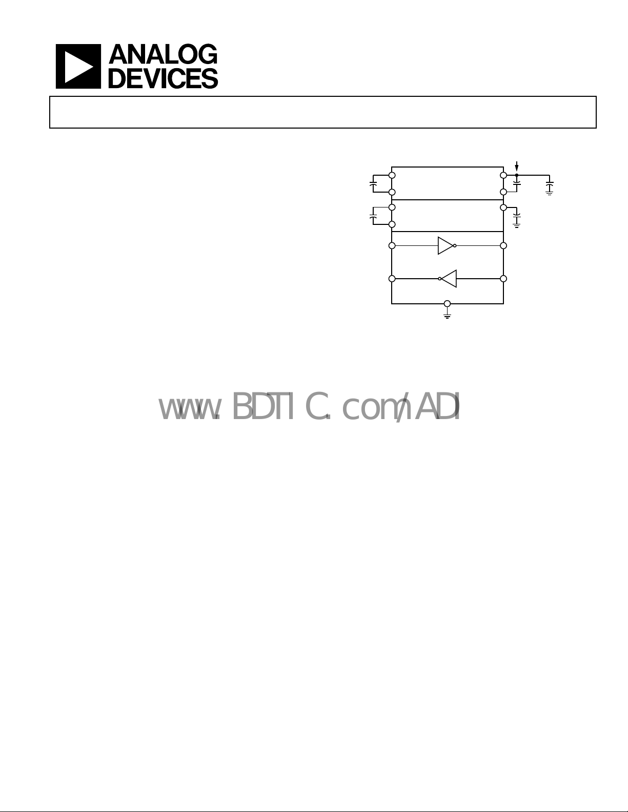
The ADM3101E is a high speed, single-channel, RS-232/
ITU-T V.28 transceiver interface device that operates from
a single 3.3 V power supply. Low power consumption makes
it ideal for battery-powered portable instruments.
The ADM3101E conforms to the EIA/TIA-232E and ITU-T V.28
specifications and operates at data rates of up to 460 kbps.
All RS-232 (T
and outputs are protected against electrostatic discharges (up
to ±15 kV ESD protection).
and RIN) and CMOS (TIN and R
OUT
) inputs
OUT
RS-232 Line Driver/Receiver
ADM3101E
FUNCTIONAL BLOCK DIAGRAM
+3.3V INPU
+
+
CMOS
INPUT
C1+
+3.3V TO +6.6V
VOLTAGE DOUBLER
C1–
C2+
+6.6V TO –6.6V
VOLTAGE INVERTER
C2–
T
IN
T
0.1µF
16V
0.1µF
16V
C1
C2
ADM3101E
R
CMOS
OUTPUT
*INTERNAL 5k PULL-DOWN
RESISTOR ON THE RS-232 INPUT.
OUT
R
GND
Figure 1.
Because of the ±15 kV ESD protection of the ADM3101E
input/output pins, this device is ideally suited for operation
in electrically harsh environments or where RS-232 cables are
frequently plugged and unplugged.
Four external 0.1 μF charge pump capacitors are used for the
voltage doubler/inverter permitting operation from a single
3.3 V supply.
The ADM3101E is available in both a 12-lead LFCSP and 16-lead
QSOP, specified over the −40°C to +85°C temperature range.
V
T
OUT
CC
V+
V–
R
IN
C3
+
0.1µF
6.3V
C4
+
0.1µF
16V
EIA/TI A-232E
OUTPUT
EIA/TI A-232E
INPUT*
+
C5
0.1µF
6766-001
Rev. C
Information furnished by Analog Devices is believed to be accurate and reliable. However, no
responsibility is assumed by Analog Devices for its use, nor for any infringements of patents or other
rights of third parties that may result from its use. Specifications subject to change without notice. No
license is granted by implication or otherwise under any patent or patent rights of Analog Devices.
Trademarks and registered trademarks are the property of their respective owners.
One Technology Way, P.O. Box 9106, Norwood, MA 02062-9106, U.S.A.
Tel: 781.329.4700 www.analog.com
Fax: 781.461.3113 ©2007–2008 Analog Devices, Inc. All rights reserved.
Page 2

ADM3101E
www.BDTIC.com/ADI
TABLE OF CONTENTS
Features .............................................................................................. 1
Applications ....................................................................................... 1
Functional Block Diagram .............................................................. 1
General Description ......................................................................... 1
Revision History ............................................................................... 2
Specifications ..................................................................................... 3
Absolute Maximum Ratings ............................................................ 4
ESD Caution .................................................................................. 4
REVISION HISTORY
7/08—Rev. B to Rev. C
Changes to General Description Section ...................................... 1
Reformatted Table 1 ......................................................................... 4
Change to T
Changes to Figure 2 .......................................................................... 5
Moved High Baud Rate Section ...................................................... 8
Added Exposed Pad Notation to Outline Dimensions ............... 9
12/07—Rev. A to Rev. B
Added 16-lead QSOP Package (Universal) ................................... 1
Updated Outline Dimensions ....................................................... 10
Changes to Ordering Guide .......................................................... 10
Rating, Table 2 ......................................................... 4
IN
Pin Configurations and Function Descriptions ............................5
Typical Performance Characteristics ..............................................6
Theory of Operation .........................................................................8
Circuit Description .......................................................................8
High Baud Rate ..............................................................................8
Outline Dimensions ..........................................................................9
Ordering Guide .............................................................................9
10/07—Rev. 0 to Rev. A
Changes to Figure 1 ........................................................................... 1
Changes to Table 1, RS-232 Receiver Section ................................ 3
Changes to Table 3 ............................................................................. 5
Changes to Figure 11 ......................................................................... 8
5/07—Revision 0: Initial Version
Rev. C | Page 2 of 12
Page 3
ADM3101E
www.BDTIC.com/ADI
SPECIFICATIONS
VCC = 3.3 V ± 0.3 V, C1 to C4 = 0.1 μF, −40°C ≤ TA ≤ +85°C, unless otherwise noted.
Table 1.
Parameter Test Conditions/Comments Min Typ Max Unit
DC CHARACTERISTICS
Operating Voltage Range 3.0 3.3 5.5 V
Power Supply Current, VCC No load 1.5 2.6 mA
R
LOGIC
Input Logic Threshold Low, V
Input Logic Threshold High, V
Input Logic Threshold Low, V
Input Logic Threshold High, V
TIN 0.6 V
INL
TIN 1.4 V
INH
TIN, VCC = 5.0 V ± 0.5 V 0.8 V
INL
TIN, VCC = 5.0 V ± 0.5 V 2.0 V
INH
CMOS Output Voltage Low, VOL I
CMOS Output Voltage High, VOH
Logic Pull-Up Current TIN = GND to VCC 5 12 μA
RS-232 RECEIVER
EIA/TIA-232E Input Voltage Range
1
−30 +30 V
EIA/TIA-232E Input Threshold Low VCC = 3.0 V to 5.5 V 0.6 1.3 V
EIA/TIA-232E Input Threshold High 1.6 2.4 V
EIA/TIA-232E Input Hysteresis 0.4 V
EIA/TIA-232E Input Resistance 3 5 7 kΩ
TRANSMITTER
Output Voltage Swing
RS-232
RS-562 VCC = 3.0 V ±4.5 V
Transmitter Output Resistance VCC = 0 V, V
RS-232 Output Short-Circuit Current ±15 mA
TIMING CHARACTERISTICS
Maximum Data Rate VCC = 3.3 V, RL = 3 kΩ to 7 kΩ, CL = 50 pF to 1000 pF 460 kbps
Receiver Propagation Delay
t
0.4 μs
PHL
t
0.4 μs
PLH
Transmitter Propagation Delay RL = 3 kΩ, CL = 1000 pF 600 ns
Transmitter Skew 80 ns
Receiver Skew 70 ns
Transition Region Slew Rate
ESD PROTECTION
RS-232 and CMOS I/O Pins Human body model air discharge ±15 kV
Human body model contact discharge ±8 kV
1
Guaranteed by design.
= 3 kΩ to GND 5 7 mA
L
= 1.6 mA 0.4 V
OUT
I
= −1 mA
OUT
= 3.3 V to 5.5 V; transmitter output loaded
V
CC
VCC − 0.6 V
±5.0 ±5.7 V
with 3 kΩ to ground
1
= ±2 V
OUT
+3 V to −3 V or −3 V to +3 V, V
R
= 3 kΩ, CL = 1000 pF, TA = 25°C
L
300 Ω
= +3.3 V,
CC
1
5.5 10 30 V/μs
Rev. C | Page 3 of 12
Page 4
ADM3101E
www.BDTIC.com/ADI
ABSOLUTE MAXIMUM RATINGS
TA = 25°C, unless otherwise noted.
Table 2.
Parameter Rating
VCC −0.3 V to +6 V
V+ (VCC − 0.3 V) to +13 V
V− +0.3 V to −13 V
Input Voltages
T
−0.3 V to (VCC + 0.3 V)
IN
RIN ±30 V
Output Voltages
T
±15 V
OUT
R
−0.3 V to (VCC + 0.3 V)
OUT
Short-Circuit Duration
T
OUT
Package Information
θJA, Thermal Impedance (LFCSP) 61.1°C/W
θJA, Thermal Impedance (QSOP) 149.97°C/W
Operating Temperature Range
Industrial (A Version) −40°C to +85°C
Storage Temperature Range −65°C to +150°C
Pb-Free Temperature (Soldering, 10 sec) 260°C
Continuous
Stresses above those listed under Absolute Maximum Ratings
may cause permanent damage to the device. This is a stress
rating only; functional operation of the device at these or any
other conditions above those indicated in the operational
section of this specification is not implied. Exposure to absolute
maximum rating conditions for extended periods may affect
device reliability.
ESD CAUTION
Rev. C | Page 4 of 12
Page 5

ADM3101E
www.BDTIC.com/ADI
PIN CONFIGURATIONS AND FUNCTION DESCRIPTIONS
C1–
C2+
C2–
12
11
10
PIN 1
INDICAT OR
1C1+
ADM3101E
2R
OUT
IN
NOTES
1. PADDLE CONNECTED TO G ND. THIS CO NNECTION IS NOT
REQUIRED TO MEET THE E LECTRICAL P ERFORMANCES.
3T
TOP VIEW
(Not to Scale)
4
5
V+
V
Figure 2. LFCSP Pin Configuration
9R
IN
8T
OUT
7V–
6
CC
GND
06766-002
1
C1–
2
C1+
3
NC
4
R
OUT
5
T
IN
6
NC
7
V+
8
V
CC
ADM3101E
TOP VIEW
(Not to Scale)
NC = NO CONNECT
16
C2+
15
C2–
14
NC
13
R
IN
12
T
OUT
11
NC
10
V–
9
GND
06766-014
Figure 3. QSOP Pin Configuration
Table 3. Pin Function Descriptions
Pin No.
LFCSP QSOP
1, 12 2, 1 C1+, C1−
Mnemonic Description
Positive and Negative Connections for Charge Pump Capacitor. External Capacitor C1 is connected
between these pins; a 0.1 μF capacitor is recommended, but larger capacitors up to 10 μF can be used.
2 4 R
Receiver Output. This pin outputs CMOS output logic levels.
OUT
3 5 TIN Transmitter (Driver) Input. This input accepts TTL/CMOS levels.
4 7 V+ Internally Generated Positive Supply (+6 V Nominal).
5 8 VCC Power Supply Input, 3.0 V to 5.5 V.
6 9 GND Ground. Must be connected to 0 V.
7 10 V– Internally Generated Negative Supply (−6 V Nominal).
8 12 T
9 13 RIN
Transmitter (Driver) Output. This pin outputs RS-232 signal levels (typically ±6 V).
OUT
Receiver Input. This input accepts RS-232 signal levels. An internal 5 kΩ pull-down resistor to GND is
connected on the input.
10, 11 15, 16 C2−, C2+
Positive and Negative Connections for Charge Pump Capacitor. External Capacitor C2 is connected
between these pins; a 0.1 μF capacitor is recommended, but larger capacitors up to 10 μF can be used.
N/A 3, 6, 11, 14 NC No Connect. These pins should always remain unconnected.
Rev. C | Page 5 of 12
Page 6

ADM3101E
www.BDTIC.com/ADI
TYPICAL PERFORMANCE CHARACTERISTICS
8
6
4
Tx OUTPUT HIGH
VCC = 3.3V
8
6
4
V+
V
CC
= 3.3V
2
0
–2
Tx OUTPUT (V)
–4
–6
–8
0 1000
Tx OUTPUT LOW
200 400 600 800
LOAD CAPACITANCE ( pF)
Figure 4. Transmitter Output Voltage High/Low vs.
Load Capacitance @ 460 kbps
15
10
Tx OUTPUT HIGH
5
0
Tx OUTPUT (V)
–5
Tx OUTPUT LOW
–10
2
0
VOLTAGE (V)
–2
–4
–6
–8
0
06766-003
V–
13
24
LOAD CURRENT (mA)
06766-006
Figure 7. Charge Pump V+, V− vs. Load Current
350
300
250
200
150
100
CHARGE PUMP IMPEDANCE ()
50
V–
V+
–15
36
45
V
(V)
CC
06766-004
Figure 5. Transmitter Output Voltage High/Low vs. VCC, RL = 3 kΩ
8
6
4
2
0
–2
Tx OUTPUT (V)
–4
–6
–8
0
1234
Tx OUTPUT HIGH
Tx OUTPUT LOW
LOAD CURRENT (mA)
VCC = 3.3V
06766-005
Figure 6. Transmitter Output Voltage High/Low vs. Load Current
0
36
Figure 8. Charge Pump Impedance vs. VCC
14
VCC = 3.3V
12
10
8
(mA)
DD
I
6
4
2
0
0 1000
200 400 600 800
Figure 9. Power Supply Current vs. Load Capacitance
45
V
(V)
CC
LOAD CAPACITANCE ( pF)
06766-007
06766-008
Rev. C | Page 6 of 12
Page 7

ADM3101E
V
V
www.BDTIC.com/ADI
5.0
4.5
1
5V/DI
2
5V/DI
VCC = 3.3V
LOAD = 3k AND 1nF
TIME (1µs/DIV)
Figure 10. 460 kbps Data Transmission
06766-009
4.0
3.5
3.0
2.5
2.0
1.5
VOLTAGE THRESHOLDS (V)
IN
1.0
T
0.5
0
3.0 5.5
3.5 4.0 4.5 5.0
V
(V)
CC
Figure 11. TIN Voltage Threshold vs. VCC
06766-010
Rev. C | Page 7 of 12
Page 8

ADM3101E
T
www.BDTIC.com/ADI
THEORY OF OPERATION
The ADM3101E is a single-channel RS-232 line driver/receiver.
Step-up voltage converters, coupled with level shifting transmitters and receivers, allow RS-232 levels to be developed while
operating from a single 3.3 V supply.
CMOS technology is used to keep the power dissipation to
an absolute minimum, allowing maximum battery life in
portable applications.
CIRCUIT DESCRIPTION
The internal circuitry consists of the following main sections:
• A charge pump voltage converter
• A 3.3 V logic to an EIA/TIA-232E transmitter
• An EIA/TIA-232E to a 3.3 V logic receiver
+3.3V INPU
+
+
CMOS
INPUT
C1+
+3.3V TO +6.6V
VOLTAGE DOUBLER
C1–
C2+
+6.6V TO –6.6V
VOLTAGE INVERTER
C2–
T
IN
T
0.1µF
16V
0.1µF
16V
C1
C2
ADM3101E
R
CMOS
OUTPUT
*INTERNAL 5k PULL-DOWN
RESISTOR ON THE RS-232 INPUT.
OUT
R
GND
Figure 12. Typical Operating Circuit
Charge Pump Voltage Converter
The charge pump voltage converter consists of a 200 kHz oscillator and a switching matrix. The converter generates a ±6.6 V
supply (when unloaded) from the 3.3 V input level. This is achieved
in two stages by using a switched capacitor technique, as illustrated
in Figure 13 and Figure 14. First, the 3.3 V input supply is doubled
to +6.6 V by using C1 as the charge storage element. The +6.6 V
level is then inverted to generate −6.6 V using C2 as the storage
element. C3 is shown connected between V+ and V
equally effective if connected between V+ and GND.
The C3 and C4 capacitors are used to reduce the output ripple.
The values are not critical and can be increased, if desired. Larger
capacitors (up to 10 μF) can also be used in place of the C1, C2,
C3, and C4 capacitors.
V
GND
CC
S1
+ +
S2
V
CC
+
V+
V–
+
T
OUT
EIA/TI A-232E
OUTPUT
R
IN
EIA/TI A-232E
INPUT*
S3
S4
C3C1
C3
0.1µF
6.3V
C4
0.1µF
16V
V+ = 2V
V
CC
but is
CC
+
CC
C5
0.1µF
6766-011
S1
S2
FROM
VOLTAGE
DOUBLER
V+
GND
INTERNAL
OSCILLATOR
Figure 14. Charge Pump Voltage Inverter
3.3 V Logic to EIA/TIA-232E Transmitter
The transmitter driver converts the 3.3 V logic input levels
into RS-232 output levels. When driving an RS-232 load with
V
= 3.3 V, the output voltage swing is typically ±6 V. Internally,
CC
pin has a weak pull-up that allows it to be driven by an
the T
IN
open-drain output, but the maximum operating data rate is
reduced when the T
pin is driven by an open-drain pin.
IN
EIA/TIA-232E to 3.3 V Logic Receiver
The receiver is an inverting level shifter that accepts the RS-232
input level and translates it into a 3.3 V logic output level. The
input has an internal 5 kΩ pull-down resistor to ground and is
protected against overvoltages of up to ±30 V. An unconnected
input is pulled to 0 V by the internal 5 kΩ pull-down resistor,
which, therefore, results in a Logic 1 output level for an unconnected input or for an input connected to GND.
The receiver has a Schmitt trigger input with a hysteresis level
of 0.4 V, which ensures error-free reception for both a noisy
input and for an input with slow transition times.
CMOS Input Voltage Thresholds
The CMOS input and output pins (TIN and R
ADM3101E are designed to interface with 1.8 V logic
thresholds when V
= 3.3 V.
CC
The CMOS input and output pins (T
ADM3101E are also designed to interface with TTL/CMOS
logic thresholds when V
= 5 V.
CC
ESD Protection on RS-232 and CMOS I/O Pins
All RS-232 (T
and RIN) and CMOS (TIN and R
OUT
and outputs are protected against electrostatic discharges (up
to ±15 kV).
HIGH BAUD RATE
The ADM3101E features high slew rates, permitting data transmission at rates well in excess of the EIA/RS-232 specifications.
The RS-232 voltage levels are maintained at data rates of up to
460 kbps, even under worst-case loading conditions, when T
driven by a push-pull output. The slew rate is internally controlled
to less than 30 V/μs to minimize EMI interference.
S3
+ +
S4
and R
IN
OUT
OUT
GND
C4C2
V– = –(V+)
) of the
) of the
) inputs
OUT
06766-013
is
IN
INTERNAL
OSCILLATOR
Figure 13. Charge Pump Voltage Doubler
06766-012
Rev. C | Page 8 of 12
Page 9

ADM3101E
S
www.BDTIC.com/ADI
OUTLINE DIMENSIONS
PIN 1
INDICATOR
3.15
3.00 SQ
2.85
TOP
VIEW
2.95
2.75 SQ
2.55
0.60 MAX
0.75
0.60
0.50
0.60 MAX
9
7
10
EXPOSED
(BOTTOM
6
PAD
VIEW)
0.50
BSC
PIN 1
12
4
INDICATOR
*
1
3
1.45
1.30 SQ
1.15
0.25 MIN
1.00
0.85
0.80
EATING
PLANE
0.065 (1.65)
0.049 (1.25)
0.010 (0.25)
0.004 (0.10)
COPLANARIT Y
0.004 (0.10)
12° MAX
0.80 MAX
0.65 TYP
0.30
0.23
0.18
*
COMPLIANT TO JEDEC STANDARDS MO-220-VEED-1
EXCEPT FO R EXPOSED PAD DI MENSION.
0.05 MAX
0.02 NOM
0.20 REF
COPLANARITY
0.08
*
PADDLE CONNECTED TO G ND.
THIS CO NNECTION I S NOT
REQUIRED TO MEET THE
ELECTRICAL PERFORMANCES.
Figure 15. 12-Lead Lead Frame Chip Scale Package [LFCSP_VQ]
3 mm × 3 mm Body, Very Thin Quad
(CP-12-1)
Dimensions shown in millimeters
0.197 (5.00)
0.193 (4.90)
0.189 (4.80)
16
1
0.025 (0.64)
BSC
9
8
0.012 (0.30)
0.008 (0.20)
0.158 (4.01)
0.154 (3.91)
0.150 (3.81)
0.069 (1.75)
0.053 (1.35)
SEATING
PLANE
0.244 (6.20)
0.236 (5.99)
0.228 (5.79)
8°
0°
0.010 (0.25)
0.006 (0.15)
0.050 (1.27)
0.016 (0.41)
0.020 (0.51)
0.010 (0.25)
0.041 (1.04)
REF
050808-B
CONTROLL ING DIMENSIONS ARE IN INCHES; MIL LIMETERS DIMENSIO NS
(IN PARENTHESES) ARE ROUNDED-O FF INCH EQ UIVALENTS FOR
REFERENCE ON LY AND ARE NOT APPROPRI ATE FOR USE IN DESIGN.
COMPLIANT TO JEDEC STANDARDS MO-137-AB
Figure 16. 16-Lead Shrink Small Outline Package [QSOP]
Dimensions shown in inches
ORDERING GUIDE
Model Temperature Range Package Description Package Option Branding
ADM3101EACPZ-REEL1−40°C to +85°C 12-Lead Lead Frame Chip Scale Package [LFCSP_VQ] CP-12-1 MA6
ADM3101EACPZ-250R7
ADM3101EARQZ
ADM3101EARQZ-REEL
1
Z = RoHS Compliant Part.
1
1
–40°C to +85°C 16-Lead Shrink Small Outline Package [QSOP] RQ-16
–40°C to +85°C 12-Lead Lead Frame Chip Scale Package [LFCSP_VQ] CP-12-1 MA6
1
–40°C to +85°C 16-Lead Shrink Small Outline Package [QSOP] RQ-16
Rev. C | Page 9 of 12
(RQ-16)
012808-A
Page 10

ADM3101E
www.BDTIC.com/ADI
NOTES
Rev. C | Page 10 of 12
Page 11

ADM3101E
www.BDTIC.com/ADI
NOTES
Rev. C | Page 11 of 12
Page 12

ADM3101E
www.BDTIC.com/ADI
NOTES
©2007–2008 Analog Devices, Inc. All rights reserved. Trademarks and
registered trademarks are the property of their respective owners.
D06766-0-7/08(C)
Rev. C | Page 12 of 12
 Loading...