

Page 1
PRELIMINARY TECHNICAL DATA
Preliminary Technical Data
REV. PrA 02/02
High-Speed (10Mbps), Fail-Safe, RS-485/RS-422
Transceivers with Slew-Rate-Limiting
a
FEATURES
Enhanced Slew Rate Limiting for Error-Free Data
Transmission
Fail-Safe Receiver Operation while Maintaining
EIA/TIA-485 compatibility
Low-Current (1nA) Shutdown Mode
High Input Impedance — Up to 256 Transceivers on Bus
±15kV ESD Protection (Human Body Model) on
RS-485 I/O pins
Pin-Compatible with Industry Standard 75176
APPLICATIONS
Enhanced Replacement for Industry-Standard Parts
EMI-Sensitive Systems
Level Translation
LANs for Industrial Control Applications
and ±15kV ESD Protection
ADM3082/ADM3085/ADM3088
GENERAL DESCRIPTION
The ADM3082/ADM3085/ADM3088 are high-speed
RS-485/RS-422 transceivers consisting of one driver and one
receiver per package. The devices feature fail-safe operation,
ensuring a logic-high receiver output when the receiver inputs are open-circuit or short-circuit. This guarantees that
the receiver output will be high if all the transmitters on a
terminated bus are disabled (high-impedance).
The ADM3082 has a slew-rate limited driver to minimize
electromagnetic interference (EMI) and reduce reflections
caused by incorrectly terminated cables. This allows errorfree transmission at data rates up to 115kbps.
The ADM3085 offers a higher slew rate allowing data rates
up to 500kbps, while the ADM3088 has a driver whose slew
rate is not limited, allowing data rates up to 10Mbps.
All devices in the family feature ±15kV electrostatic discharge (ESD) protection and high receiver input impedance (1/8 unit load), allowing up to 256 transceivers on
the bus. The devices have low current drain of 375µA unloaded, or fully loaded with the drivers disabled, and feature an ultra-low power (1nA) shutdown mode.
Information furnished by Analog Devices is believed to be accurate and
reliable. However, no responsibility is assumed by Analog Devices for its
use, nor for any infringements of patents or other rights of third parties
which may result from its use. No license is granted by implication or
otherwise under any patent or patent rights of Analog Devices.
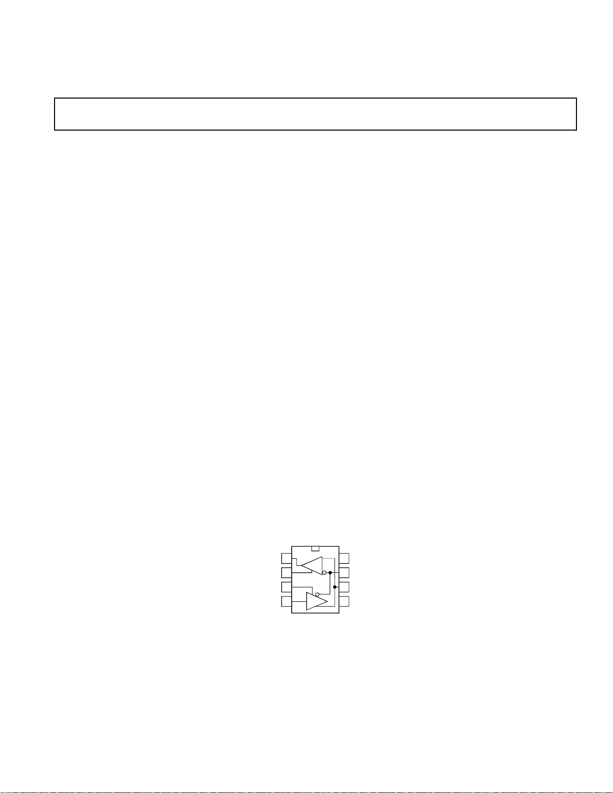
FUNCTIONAL BLOCK DIAGRAM
RO
1
R
2
RE
3
DE
4
DI
ADM3082/ADM3085/ADM3088
D
V
8
CC
7
B
6
A
GND
5
One Technology Way, P.O. Box 9106, Norwood, MA 02062-9106, U.S.A.
Tel: 617/329-4700World Wide Web Site: http://www.analog.com
Fax: 617/326-8703 © Analog Devices, Inc., 2002
Page 2

PRELIMINAR Y TECHNICAL DA T A
REV. PrA 02/02
ADM3082/ADM3085/ADM3088
ADM3082/ADM3085/ADM3088 SPECIFICATIONS
DC ELECTRICAL CHARACTERISTICS
(VCC = +5V ±5%, TA = T
DRIVER
Parameter Min Typ Max Units Test Conditions/Comments
MIN
to T
, unless otherwise noted. Typical values are at VCC = +5V and TA = +25°C.) (Note 1)
MAX
Differential Driver Output, V
Differential Driver Output,V
OD1
OD2
2.0 V Figure 1, R = 50V (RS-422)
5 V Figure 1 (No Load)
1.5 V Figure 1, R = 27V (RS-485)
Change-in-Magnitude of Differential 0.2 V Figure 1, R = 50V or R = 27V
Common-Mode Output Voltage, DV
OD
(Note 2)
Driver Common-Mode 3 V Figure 1, R = 50V or R = 27V
Output Voltage, V
OC
Change-in-Magnitude of 0.2 V Figure 1, R = 50V or R = 27V
Common-Mode Voltage, DV
Input High Voltage,V
IH1
OC
2.0 V
(Note 2)
(DE, DI, RE)
Input Low Voltage, V
lL1
0.8 V
(DE, DI, RE)
DI Input Hysteresis, V
Input Current, I
Input Current (A and B), I
HYS
(DE, DI, RE)±2µA
IN1
IN4
100 mV
125 µA DE = GND, V
–75 µ A DE = GND, V
V
IN
= 12V
= GND or 5.25V,
CC
= GND or 5.25V,
CC
VIN = –7V
Output Leakage (Y and Z), 125 µA DE = GND, V
Full Duplex, I
O
VIN = 12V
–100 µA DE = GND, V
= GND or 5.25V,
CC
= GND or 5.25V,
CC
VIN = –7V
Driver Short-Circuit,V
OD1
–250 mA –7V # V
Output Current 250 mA 0V # V
±25 mA 0V # V
–2–
# VCC (Note 3)
OUT
# 12V (Note 3)
OUT
# VCC (Note 3)
OUT
Page 3

PRELIMINAR Y TECHNICAL DA T A
REV. PrA 02/02
ADM3082/ADM3085/ADM3088
ADM3082/ADM3085/ADM3088 SPECIFICATIONS (continued)
DC ELECTRICAL CHARACTERISTICS
(VCC = +5V ±5%, TA = T
RECEIVER
Parameter Min Typ Max Units Test Conditions/Comments
MIN
to T
, unless otherwise noted. Typical values are at VCC = +5V and TA = +25°C.) (Note 1)
MAX
Receiver Differential Threshold –200 –125 –50 mV –7V # V
Voltage, V
Receiver Input Hysteresis, DV
Receiver Output High Voltage, V
Receiver Output Low Voltage, V
TH
TH
OL
OH
25 mV
VCC –1 .5 V IO = -4mA, VID = -50mV
0.4 V IO = 4mA, VID = -200mV
# 12V
CM
Three-State Output Current at ±1 µA 0.4V # VO # 2.4V
Receiver, I
Receiver Input Resistance, R
Receiver Output Short-Circuit ±7 ±95 mA 0V # VRO # V
Current, I
OZR
OSR
IN
96 kV –7V # VCM # 12V
CC
SUPPLY CURRENT
Parameter Min Typ Max Units Test Conditions/Comments
Supply Current, I
CC
430 900 µA No load, RE = DI = GND or VCC,
DE = V
CC
375 600 µA No load, RE = DI = GND or VCC,
DE = GND
Supply Current in 0.001 10 µ A DE = GND, VRE = V
Shutdown Mode, I
SHDN
CC
ESD Protection for Y, Z, A, B ±15 kV Human Body Model
NOTES
1
All currents into the device are positive; all currents out of the device are negative. All voltages are referred to device ground unless otherwise noted.
2
DDO and DVCC are the changes in VOD and VOC, respectively, when the DI input changes state.
3
Maximum current level applies to peak current just prior to foldback-current limiting; minimum current level applies during current limiting.
–3–
Page 4

PRELIMINAR Y TECHNICAL DA T A
REV. PrA 02/02
ADM3082/ADM3085/ADM3088
ADM3082/ADM3085/ADM3088 SPECIFICATIONS (continued)
SWITCHING CHARACTERISTICS—ADM3082
(VCC = +5V ±5%, TA = T
Parameter Min Typ Max Units Test Conditions/Comments
MIN
to T
, unless otherwise noted. Typical values are at VCC = +5V and TA = +25°C.) (Note 1)
MAX
Driver Input-to-Output, t
Driver Input-to-Output, t
Driver Output Skew,|t
Driver Rise or Fall Time, t
Maximum Data Rate, f
Driver Enable to Output High, t
Driver Enable to Output Low, t
Driver Disable Time from Low, t
Driver Disable Time from High, t
Receiver Input to Output, t
Differential Receiver Skew, t
|t
- t
RPLH
| rise and fall time of VID # l5ns
RPHL
Receiver Enable to Output Low, t
DPLH
DPHL
DPLH-tDPHL
, t
DR
MAX
RPLH
RSKD
, t
|, t
DF
DZH
DZL
DLZ
DHZ
RPHL
RZL
DSKEW
500 2030 2600 ns Figures 2 and 3, R
500 2030 2600 ns CL1 = CL2 = 100pF
–3 ±200 ns Figures 2 and 3, R
CL1 = CL2 = 100pF
667 1320 2500 ns Figures 2 and 3, R
CL1 = CL2 = 100pF
115 kbps
3500 ns Figures 5 and 6, CL = 100pF,
S2 closed
3500 ns Figures 5 and 6, CL = 100pF,
S1 closed
100 ns Figures 5 and 6, CL = l5pF,
S1 closed
100 ns Figures 4 and 5, CL = l5pF,
S2 closed
127 200 ns Figure 7; |VID| $ 2.0V;
rise and fall time of VID # l5ns
3 ±30 ns Figure 7; |VID| $ 2.0V;
20 50 ns Figures 7 and 8; CL = 100pF,
S1 closed
DIFF
DIFF
DIFF
= 54V,
= 54V,
= 54V,
Receiver Enable to Output High, t
RZH
20 50 ns Figures 7 and 8, CL = 100pF,
S2 closed
Receiver Disable Time from Low, t
RLZ
20 50 ns Figures 7 and 8, CL = 100pF,
S1 closed
Receiver Disable Time from High, t
RHZ
20 50 ns Figures 7 and 8 CL = 100pF,
S2 closed
Time to Shutdown, t
SHDN
Driver Enable from Shutdown to 6000 ns Figures 5 and 6, C
Output High, t
DZH(SHDN)
Driver Enable from Shutdown to 6000 ns Figures 5 and 6, C
Output Low, t
DZL(SHDN)
50 200 600 ns (Note 5)
S2 closed
S1 closed
= l5pF,
L
= l5pF,
L
Receiver Enable from Shutdown 3500 ns Figures 7 and 8, CL = 100pF,
to Output High, t
RZH(SHDN)
S2 closed
Receiver Enable from Shutdown 3500 ns Figures 7 and 8, CL = 100pF,
to Output Low, t
RZL(SHDN)
S1 closed
–4–
Page 5

PRELIMINAR Y TECHNICAL DA T A
REV. PrA 02/02
ADM3082/ADM3085/ADM3088
ADM3082/ADM3085/ADM3088 SPECIFICATIONS (continued)
SWITCHING CHARACTERISTICS—ADM3085
(VCC = +5V ±5%, TA = T
Parameter Min Typ Max Units Test Conditions/Comments
MIN
to T
, unless otherwise noted. Typical values are at VCC = +5V and TA = +25°C.) (Note 1)
MAX
Driver Input-to-Output, t
Driver Input-to-Output, t
Driver Output Skew,|t
Driver Rise or Fall Time, t
Maximum Data Rate, f
Driver Enable to Output High, t
Driver Enable to Output Low, t
Driver Disable Time from Low, t
Driver Disable Time from High, t
Receiver Input to Output, t
Differential Receiver Skew, t
|t
- t
RPLH
| rise and fall time of VID # l5ns
RPHL
Receiver Enable to Output Low, t
DPLH
MAX
DPLH
DPHL
- t
DR
RPLH
DPHL
, t
, t
RSKD
|, t
DF
DZH
DZL
DLZ
DHZ
RPHL
RZL
DSKEW
250 720 1000 ns Figures 2 and 3 R
DIFF
250 720 1000 ns CL1 = CL2 = 100pF
–3 ±100 ns Figures 2 and 3, R
CL1 = CL2 = 100pF
200 530 750 ns Figures 2 and 3, R
CL1 = CL2 = 100pF
500 kbps
2500 ns Figures 5 and 6, CL = 100pF,
S2 closed
2500 ns Figures 5 and 6, CL = 100pF,
S1 closed
100 ns Figures 5 and 6, CL = l5pF,
S1 closed
100 ns Figures 5 and 6, CL = l5pF,
S2 closed
127 200 ns Figure 7; |VID| $ 2.0V;
rise and fall time of VID # l5ns
3 ±30 ns Figure 7; |VID| $ 2.0V;
20 50 ns Figures 7 and 8 CL = 100pF,
S1 closed
= 54V,
DIFF
DIFF
= 54V,
= 54V,
Receiver Enable to Output High, t
RZH
20 50 ns Figures 7 and 8, CL = 100pF,
S2 closed
Receiver Disable Time from Low, t
RLZ
20 50 ns Figures 7 and 8, CL = 100pF,
S1 closed
Receiver Disable Time from High, t
RHZ
20 50 ns Figures 7 and 8, CL = 100pF,
S2 closed
Time to Shutdown, t
SHDN
50 200 600 ns (Note 5)
Driver Enable from Shutdown 4500 ns Figures 5 and 6, CL = l5pF,
to Output High, t
DZH(SHDN)
S2 closed
Driver Enable from Shutdown 4500 ns Figures 5 and 6, CL = l5pF,
to Output Low, t
OZL(SHDN)
Receiver Enable from Shutdown 3500 ns Figures 7 and 8, C
to Output High, t
RZH(SHDN)
Receiver Enable from Shutdown 3500 ns Figures 7 and 8, C
to Output Low, t
RZL(SHDN)
S1 closed
S2 closed
S1 closed
= 100pF,
L
= 100pF,
L
–5–
Page 6

PRELIMINAR Y TECHNICAL DA T A
REV. PrA 02/02
ADM3082/ADM3085/ADM3088
ADM3082/ADM3085/ADM3088 SPECIFICATIONS (continued)
SWITCHING CHARACTERISTICS—ADM3088
(VCC = +5V ±5%, TA = T
Parameter Min Typ Max Units Test Conditions/Comments
MIN
to T
, unless otherwise noted. Typical values are at VCC = +5V and TA = +25°C.) (Note 1)
MAX
Driver Input-to-Output, t
Driver Input-to-Output, t
Driver Output Skew,|t
DPLH
DPHL
DPLH -tDPHL
|, t
DSKEW
34 60 ns Figures 2 and 5, R
34 60 ns CL1 = CL2 = 100pF
–2.5 ±10 ns Figures 2 and 5, R
CL1 = CL2 = 100pF
Driver Rise or Fall Time, tDR, tDF 14 25 ns Figures 7 and 9, R
CL1 = CL2 = 100pF
Maximum Data Rate, f
Driver Enable to Output High, t
MAX
DZH
10 Mbps
150 ns Figures 5 and 6, CL = 100pF,
S2 closed
Driver Enable to Output Low, t
DZL
150 ns Figures 5 and 6, CL = 100pF,
S1 closed
Driver Disable Time from Low, t
DLZ
100 ns Figures 5 and 6, CL = l5pF,
S1 closed
Driver Disable Time from High, t
DHZ
100 ns Figures 5 and 6, CL = l5pF,
S2 closed
Receiver Input-to-Output, t
RPLH
, t
RPHL
106 150 ns Figure 7; |VID| $ 2.0V;
rise and fall time of VID # l5ns
DifferentialReceiver Skew, t
|t
– t
RPLH
| rise and fall time of VID # l5ns
RPHL
Receiver Enable to Output Low, t
RSKD
RZL
0 ±10 ns Figures 7; |VID| $ 2.0V;
20 50 ns Figures 7 and 8, CL = 100pF,
S1 closed
DIFF
DIFF
DIFF
= 54V,
= 54V,
= 54V,
Receiver Enable to Output High, t
RZH
20 50 ns Figures 7 and 8, CL = 100pF,
S2 closed
Receiver Disable Time from Low, t
RLZ
20 50 ns Figures 7 and 8, CL = 100pF,
S1 closed
Receiver Disable Time from High, t
RHZ
20 50 ns Figures 7 and 8, CL = 100pF,
S2 closed
Time to Shutdown, t
SHDN
50 200 600 ns (Note 5)
Driver Enable from Shutdown 250 ns Figures 5 and 6, CL = l5pF,
toOutput High, t
DZH(SHDN)
S2 closed
Driver Enable from Shutdown 250 ns Figures 5 and 6, CL = l5pF,
to Output Low, t
DZL(SHDN)
S1 closed
Receiver Enable from Shutdown 3500 ns Figures 7 and 8, CL = 100pF,
to Output High, t
RZH(SHDN)
Receiver Enable from Shutdown 3500 ns Figures 7 and 8, C
to Output Low, t
NOTES
5
The device is put into shutdown by bringing RE high and DE low. If the enable inputs are in this state for less than 50ns, the device is guaranteed not to enter shut-
down. If the enable inputs are in this state for at least 600ns, the device is guaranteed to have entered shutdown.
RZL(SHDN)
S2 closed
S1 closed
= 100pF,
L
–6–
Page 7

PRELIMINAR Y TECHNICAL DA T A
REV. PrA 02/02
ADM3082/ADM3085/ADM3088
ADM3082/ADM3085/ADM3088 TEST CIRCUITS AND TIMING
500
V
CC
S1
V
S2
Y
R
V
OD
R
Z
V
OC
Figure 1. Driver DC Load Test Circuit
OUTPUT
UNDER
TEST
C
15pF
TEST
POINT
RL
3V
DE
DI
V
OD2
R
DIFF
Figure 2. Test Load for Driver Timing Tests
5V
DI
V
DIFF
1.5V
0V
Z
V
0
Y
V
0
0
10%
-V
0
t
DPLH
/2
V
0
V
= VY - V
90%
DIFF
t
DR
t
SKEW
= |t
Z
DPLH-tDPHL
|
Figure 3. Driver Propagation Delays
t
DPHL
Figure 5. Test Load for Driver Enable/Disable Time Test
C
L1
C
L2
5V
DE
Y, Z
V
Y, Z
V
0V
OL
OL
t
DZL(SHDN )
2.3V
2.3V
t
DZH(SHDN) tDZH
, t
DZL
OUTPUT NORMALLY LOW
OUTPUT NORMALLY HIGH
1.5V
t
DLZ
VOL+0.5V
VOH-0.5V
t
DHZ
Figure 6. Driver Enable and Disable Times
V
CC
TEST
C
15pF
POINT
RL
90%
10%
t
DF
RO
1kV
S1
S2
A
B1V-1V
t
RPHL
RO
V
OH
V
OL
Figure 4. Receiver Propagation Delays
t
RPLH
1.5V
1kV
Figure 7. Test Load for Receiver Enable/Disable Time Test
5V
RE
RO
RO
0V
V
CC
0V
1.5V
1.5V
, t
t
RZL(SHDN)
RZL
OUTPUT NORMALLY LOW
OUTPUT NORMALLY HIGH
t
, t
RZH(SHDN)
RZH
t
RLZ
t
RHZ
Figure 8. Receiver Enable and Disable Delay Times
–7–
V
1.5V
V
OL
OH
+0.5V
-0.5V
Page 8

PRELIMINAR Y TECHNICAL DA T A
REV. PrA 02/02
ADM3082/ADM3085/ADM3088
ABSOLUTE MAXIMUM RATINGS
Supply Voltage (VCC) . . . . . . . . . . . . . . . . . . . . . . . . . . + 7 V
Logic Input Voltage . . . . . . . . . . . . –0.3V to (V
+0.3V)
CC
Driver Output Voltage (A, B) . . . . . . . . . . . . . . . . . . ±13V
Receiver Input Voltage (A, B) . . . . . . . . . . . . . . . . . . ±13V
Receiver Input Voltage, Full Duplex (A, B) . . . . . . ±13V
Receiver Output Voltage (RO) . . . –0.3V to (V
+0.3V)
CC
Continuous Power Dissipation
8-Pin Plastic DIP
(derate 9.09mW/
8-Pin Plastic SO
(derate 5.88mW/
Maximum Junction Temperature (T
o
C above +70oC) . . . . . . . . . . . 727mW
o
C above +70oC) . . . . . . . . . . . 471mW
max) . . . . . . .150 °C
J
Storage Temperature Range . . . . . . . . .–65°C to +150°C
Lead Temperature, Soldering
Vapor Phase 60 sec . . . . . . . . . . . . . . . . . . . . . . . . . +215°C
Infra-Red 15 sec . . . . . . . . . . . . . . . . . . . . . . . . . . . +200°C
*Stresses above those listed under “Absolute Maximum Ratings” may cause permanent
damage to the device. This is a stress rating only; functional operation of the device
at these or any other conditions above those indicated in the operational section of this
specification is not implied. Exposure to absolute maximum rating conditions for
extended periods may affect device reliability.
THERMAL CHARACTERISTICS
8-Pin Plastic DIP Package
θ
= tbd K/Watt, θ
JA
= tbd K/Watt
JC
8-Pin Plastic SO Package
θ
= tbd K/Watt, θ
JA
= tbd K/Watt
JC
PIN CONFIGURATION
RO
RE
DE
DI
1
ADM3088/
2
ADM3085/
ADM3088
3
TOP VIEW
(Not to Scale)
4
V
8
CC
7
B
6
A
GND
5
ORDERING INFORMATION
Model Temperature Range Package Option
ADM3082JN 0°C to +70°C 8 Pin Plastic DIP
ADM3082JR 0°C to +70°C 8 Pin SO
ADM3082AN –40°C to +85°C 8 Pin Plastic DIP
ADM3082AR –40°C to +85°C 8 Pin SO
ADM3085JN 0°C to +70°C 8 Pin Plastic DIP
ADM3085JR 0°C to +70°C 8 Pin SO
ADM3085AN –40°C to +85°C 8 Pin Plastic DIP
ADM3085AR –40°C to +85°C 8 Pin SO
ADM3088JN 0°C to +70°C 8 Pin Plastic DIP
ADM3088JR 0°C to +70°C 8 Pin SO
ADM3088AN –40°C to +85°C 8 Pin Plastic DIP
ADM3088AR –40°C to +85°C 8 Pin SO
ADM3082/ADM3085/ADM3088 TYPICAL PERFORMANCE CHARACTERISTICS
AWA
IN G DA
IT
TA
AWA
IT IN G DA
TA
IT IN G DA
AWA
TA
TPC1. No-load Supply Current vs.
Temperature
TPC2. Output Current vs. Receiver Out-
put High Voltage
–8–
TPC3. Output Current vs. Receiver Out-
put Low Voltage
Page 9

PRELIMINAR Y TECHNICAL DA T A
REV. PrA 02/02
ADM3082/ADM3085/ADM3088
ADM3082/ADM3085/ADM3088 TYPICAL PERFORMANCE CHARACTERISTICS (continued)
TA
IT IN G DA
AWA
TPC4. Receiver Output High
Voltage vs. Temperature
TA
IN G DA
IT
TA
IT IN G D A
AWA
TPC5. Receiver Output Low
Voltage vs. Temperature
TA
IT IN G DA
TA
IT IN G DA
AWA
TPC6. Shutdown Current vs.
Temperature
TA
IT IN G D A
AWA
TPC7. ADM3082 Driver Propagation
Delay vs. Temperature
TA
IT IN G DA
AWA
TPC10. ADM3082/5 ReceIver
Propagation Delay vs. Temperature
AWA
TPC8. ADM3085 Driver Propagation
Delay vs. Temperature
TA
IN G DA
IT
AWA
TPC11. ADM3088 Receiver
Propagation Delay vs. Temperature
AWA
TPC9. ADM3088 Driver Propagation
Delay vs. Temperature
TA
IN G DA
IT
AWA
TPC12. Driver Differential Output Volt-
age vs. Temperature
–9–
Page 10

PRELIMINAR Y TECHNICAL DA T A
REV. PrA 02/02
ADM3082/ADM3085/ADM3088
ADM3082/ADM3085/ADM3088 TYPICAL PERFORMANCE CHARACTERISTICS (continued)
TA
IN G DA
IT
AWA
TPC13. Driver Output Current vs. Dif-
ferential Output Voltage
TA
IT IN G DA
AWA
TA
IT IN G DA
AWA
TPC14. Output Current vs. Driver Out-
put High Voltage
TA
IN G DA
IT
AWA
TA
IN G D A
IT
AWA
TPC15. Output Current vs. Driver Out-
put Low Voltage
TA
IT IN G DA
AWA
TPC16. ADM3082 Driver Propagation
TPC17. ADM3085 Driver Propagation
Delay
TA
IT IN G DA
AWA
TPC19. ADM3082/5 Receiver Propaga-
tion Delay
Delay
TPC18. ADM3088 Driver Propagation
Delay
TA
IT IN G D A
AWA
TPC20. ADM3088 Receiver
Propagation Delay
–10–
Page 11

PRELIMINAR Y TECHNICAL DA T A
REV. PrA 02/02
ADM3082/ADM3085/ADM3088
PIN FUNCTION DESCRIPTION
Pin Mnemonic Description
1 R O Receiver Output. When RE is low and A - B $ (more positive than) –50mV, RO will be high.
When RE is low and A – B # (more negative than) –200mV, RO will be low.
2 RE Receiver Output Enable. Take RE low to enable RO; RO is high impedance when RE is high.
Take RE high and DE low to enter low-power shutdown mode.
3 D E Driver Output Enable. Take DE high to enable driver outputs. These outputs are high
impedance when DE is low. Take RE high and DE low to enter low-power shutdown mode.
4 D I Driver Input. With DE high, a low on DI forces non-inverting output low and inverting output
high. Similarly, a high on DI forces non-inverting output high and inverting output low.
5 GND Ground
6 A Non-Inverting Receiver Input and Non-Inverting Driver Output
7 B Inverting Receiver Input and Inverting Driver Output
8V
CC
TRANSMITTING
INPUTS OUTPUTS
RE DE DI B/Z A/Y
X11 0 1
X10 1 0
0 0 X High-Z High-Z
1 0 X Shutdown
Positive Supply 4.75V =VCC =5.25V
DEVICE TRUTH TABLES
RECEIVING
INPUTS OUTPUT
RE
0X$ -0.05V 1
0X# -0.2V 0
0 X Open/shorted 1
1 1 X High-Z
1 0 X Shutdown
X = Don’t care
Shutdown mode, driver and receiver outputs high impedance
DEDE
DE
DEDE
A-BA-B
A-B
A-BA-B
RORO
RO
RORO
–11–
Page 12

PRELIMINAR Y TECHNICAL DA T A
REV. PrA 02/02
ADM3082/ADM3085/ADM3088
DETAILED DESCRIPTION
The ADM3082, ADM3085 and ADM3088 are highspeed RS-485/RS-422 transceivers offering enhanced performance over industry-standard devices All devices in the
family contain one driver and one receiver, but there is a
choice of performance options. The devices feature failsafe operation, which means that a logic-high receiver output is guaranteed when the receiver inputs are open-circuit
or short-circuit, or when they are connected to a terminated transmission line with all drivers disabled (see the
section on Fail-Safe Operation).
SLEW RATE CONTROL
The ADM3082 features a controlled slew-rate driver that
minimize electromagnetic interference (EMI) and reduce
reflections caused by incorrectly terminated cables, allowing error-free data transmission rates up to 115kbps (see
the section on Reduced EMI and Reflections).
The ADM3085 offers a higher limit on driver output
slew-rate, allowing data transmission rates up to 500kbps.
The driver slew rate of the ADM3088 is not limited, offering data transmission rates up to 10Mbps.
RECEIVER INPUT FILTERING
The receivers of all devices incorporate input hysteresis.
In addition, when operating in 115kbps or 500kbps mode,
the receivers of the ADM3082 and ADM3085 incorporate
input filtering. This enhances noise immunity with differential signals that have very slow rise and fall times, but it
does increase propagation delay by 20%.
HALF-/FULL-DUPLEX OPERATION
The ADM3082, ADM3085, and ADM3088 are dedicated
half-duplex devices (driver outputs internally linked to receiver inputs). Figure 29 shows a typical half-duplex connection between two devices.
THREE-STATE BUS CONNECTION
All the devices have a Driver Enable pin (DE) that enables the driver outputs when taken high or puts the driver
outputs into a high-impedance state when taken low. This
allows several driver outputs to be connected to an
RS-422/RS-485 bus.
Similarly, all the devices have a (active-low) Receiver Enable pin (RE). Taking this low enables the receiver, while
taking it high puts the receiver outputs into a high-impedance state. This allows several receiver outputs to be connected to a serial data bus.
HIGH INPUT IMPEDANCE
The input impedance of the devices is 96kV, which is 8
times higher than the standard RS-485 load of 12kV. A
standard driver can driver 32 standard loads, so up to 256
ADM308X receivers, or a combination of ADM308X and
other devices up to 32 unit loads, may be connected to an
RS-422/RS485 bus driven by a single driver.
SHUTDOWN MODE
All the devices have a low power shutdown mode that is
enabled by taking RE high and DE low.
If shutdown mode is not used, the fact that DE is activehigh and RE is active-low offers a convenient way of
switching the device between transmit and receive, by tying DE and RE together. This is useful, for example, in
applications using half duplex operation and where several
receiver outputs are connected to a serial bus.
The device is guaranteed not to enter shutdown mode if
DE and RE are driven in this way. If DE is low and RE is
high for less than 50ns the device will not enter shutdown.
If DE is low and RE is high for greater than 600ns, the
device is guaranteed to enter shutdown.
FAIL-SAFE OPERATION
The ADM3082/ADM3085/ADM3088 offer true fail-safe
operation while remaining fully compliant with the
±200mV EIA/TIA-485 standard. A logic-high receiver
output is guaranteed when the receiver inputs are shorted
together or open-circuit, or when they are connected to a
terminated transmission line with all drivers disabled.
This is done by setting the receiver threshold between
-50mV and –200mV. If the differential receiver input voltage (A–B) is greater than or equal to –50mV, RO is logic
high. If A–B is less than or equal to –200mV, RO is logic
low. In the case of a terminated bus with all transmitters
disabled, the receiver’s differential input voltage is pulled
to 0V by ADM308X family, which results in a logic high
with a 50mV minimum noise margin.
ENHANCED ESD PROTECTION
All Analog Devices parts incorporate protection against
electrostatic discharge (ESD) to protect the devices during handling, assembly and normal operation. In addition,
the ADM308X family has enhanced ESD protection up to
±15kV on the receiver inputs and driver outputs (A, B) to
protect against severe operational conditions such as line
transients, connection and disconnection.
+5V
)
(V
CC
RECEIVER
OUTPUT (RO)
RECEIVER
ENABLE (RE)
DRIVER
ENABLE (DE)
DATA
IN (DI)
1
2
3
4
D
ADM3082/5/8 ADM3082/5/8
8
R
7
6
5
100n
R
T
+5V
)
(V
CC
100n
5
6
R
T
7
8
D
R
4
3
2
1
DATA
IN (DI)
DRIVER
ENABLE (DE)
RECEIVER
ENABLE (RE)
RECEIVER
OUTPUT (RO)
Figure 29. Half-Duplex Configuration for ADM3082, ADM3085 or ADM3088
–12–
Page 13

PRELIMINAR Y TECHNICAL DA T A
REV. PrA 02/02
CURRENT LIMIT AND THERMAL SHUTDOWN
The ADM3082/ADM3085/ADM3088 incorporate two
protection mechanisms to guard the drivers against shortcircuits, bus contention or other fault conditions. The first
is a foldback current-limited output stage that protects the
driver against short-circuits over the entire common-mode
voltage range. The second is a thermal shutdown circuit
that puts the driver outputs into a high-impedance state if
the die temperature exceeds a safe limit.
ADM3082/ADM3085/ADM3088
TA
IN G DA
IT
REDUCED EMI AND REFLECTIONS
The ADM3082 and ADM3085 incorporate slew-rating limiting in the drivers. This reduces reflections due to incorrect cable termination and minimizes electromagnetic
interference (EMI).
Figures 9 to 11 show driver output waveforms and Fourier
analyses of 20kHz signals for the three different slew-rate
settings. It can be seen that the harmonic content is greatly
reduced for the ADM3085 and still further for the
ADM3082 (Figures 10 and 9 respectively).
TA
IN G DA
IT
AWA
AWA
Figure 11. ADM3088 Driver Output Waveform and FFT Plot
The length of an unterminated stub that can be driven
with only minor reflections depends on the rise time of
the transmitter. A conservative estimate for this is given
by the following equation:
L (metres) = t
where t
sult by 3.28 for answer in feet).
For example, the rise time of the ADM3082 is typically
1320ns, which results in acceptable waveforms with stub
lengths up to 27 metres. This is not the ultimate limit on
unterminated stub length, as a system can still work if the
waveformis allowed to settle before sampling the data.
The RS-485/RS-422 standard covers line lengths up to
4000 feet (1219 metres). Driver output and receiver output waveforms for the three slew rate settings, driving a
4000 foot cable, are shown in figures 12 to 14.
is the transmitter’s rise time in ns (multiply re-
R
/ 49.2
R
Figure 9 ADM3082 Driver Output Waveform and FFT Plot
Figure 10. ADM3085 Driver Output Waveform and FFT Plot
AWA
IN G DA
IT
TA
TA
IT IN G DA
AWA
Figure 12. Driver Input, Driver Output and Receiver Output
Waveforms of ADM3082, Driving 4000ft (1219m) of Cable
at 50kHz
–13–
Page 14

PRELIMINAR Y TECHNICAL DA T A
REV. PrA 02/02
ADM3082/ADM3085/ADM3088
TA
APPLICATIONS
Figures 15 shows a typical application of the device on a
half--duplex network. The line should be terminated at
both ends to minimize reflections and any stubs off the
main line should be kept as short as possible.
120V
IT IN G DA
AWA
Figure 13. Driver Input, Driver Output and Receiver Output
Waveforms of ADM3085, Driving 4000ft (1219m) of Cable
at 50kHz
TA
IT IN G DA
AWA
Figure 14. Driver Input, Driver Output and Receiver Output
Waveforms of ADM3088, Driving 4000ft (1219m) of Cable
at 200kHz
For line lengths in excess of 1220 metres the line should
be split into smaller sections with intermediate repeaters.
RO
RE
DE
DI
RO
RE
DE
DI
RO
RE
DE
DI
RO
RE
DE
DI
ADM3082, ADM3084, ADM 3085
OR ADM3089 WITH H/F = V
R
B
A
D
R
B
A
D
R
B
A
D
R
B
A
D
120V
CC
Figure 15. Typical Half-Duplex Network Application
0.210 (5.33)
0.160 (4.06)
0.115 (2.93)
OUTLINE DIMENSIONS
Dimensions shown in inches and (mm).
8-Pin Plastic Dual-In-Line Package (N-8)
0.430 (10.92)
0.348 (8.84)
8
14
MAX
0.022 (0.558)
0.014 (0.356)
PIN 1
0.100
(2.5 4 )
BSC
5
0.280 (7.11)
0.240 (6.10)
0.060 (1.52)
0.015 (0.38)
0.070 (1.77)
0.045 (1.15)
0.130
(3.3 0 )
MIN
SEATING
PLANE
0.325 (8.25)
0.300 (7.62)
0.195 (4.95)
0.115 (2.93)
0.015 (0.381)
0.008 (0.204)
8-Pin SO Package (R-8)
0.1968 (5.00)
0.1890 (4.80)
0.2440 (6.20)
0.2284 (5.80)
0.0098 (0.25)
0.0040 (0.10)
SEATING
PLANE
85
PIN 1
0.0500
(1.2 7 )
BSC
0.1574 (4.00)
0.1497 (3.80)
41
0.102 (2.59)
0.094 (2.39)
0.0192 (0.49)
0.0138 (0.35)
0.0098 (0.25)
0.0075 (0.19)
0.0196 (0.50)
0.0099 (0.25)
8
0
0.0500 (1.27)
0.0160 (0.41)
–14–
x 45
 Loading...