

Page 1
Isolated CAN Transceiver with Integrated
V
High Voltage, Bus-Side, Linear Regulator
FEATURES
5 kV rms isolated CAN transceiver
Integrated V
Bus side powered by V
11 V to 25 V operation on V
5 V or 3.3 V operation on V
Complies with ISO 11898 standard
High speed data rates up to 1 Mbps
Short-circuit protection on bus pins
Integrated bus miswire protection
Unpowered nodes do not disturb the bus
110 or more nodes on the bus
Thermal shutdown protection
High common-mode transient immunity: >25 kV/μs
Safety and regulatory approvals
UL recognition (pending)
5000 V
VDE Certificates of Conformity (pending)
DIN V VDE V 0884-10 (VDE V 0884-10):2006-12
V
Industrial operating temperature range: −40°C to +85°C
Wide body, 16-lead SOIC package
linear regulator
+
for 1 minute per UL 1577
RMS
= 846 V peak
IORM
and V
+
+
DD1
−
ADM3052
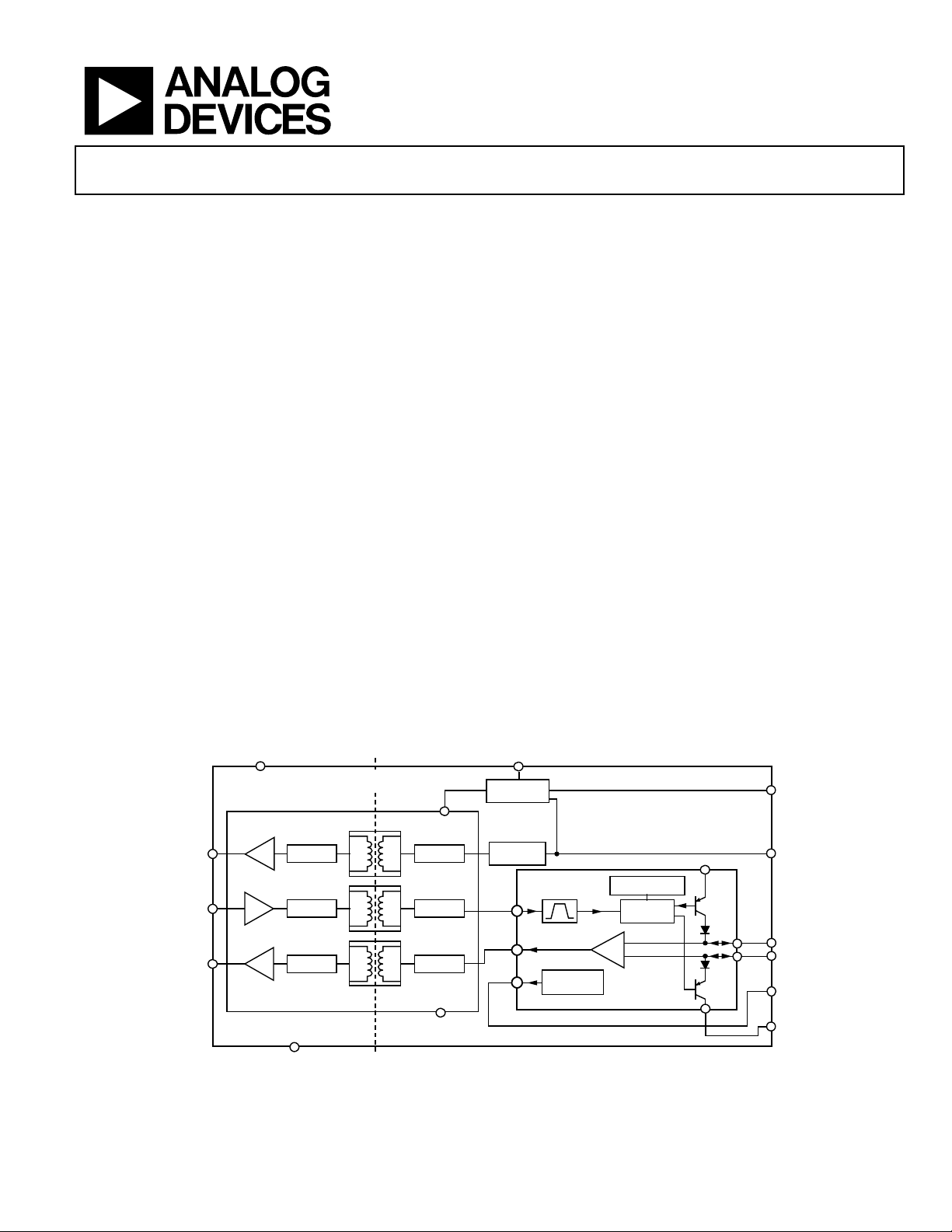
GENERAL DESCRIPTION
The ADM3052 is an isolated controller area network (CAN)
physical layer transceiver with a V
The ADM3052 complies with the ISO 11898 standard.
The device employs Analog Devices, Inc., iCoupler® technology
to combine a 3-channel isolator, a CAN transceiver, and a linear
regulator into a single package. The power is isolated between a
single 3.3 V or 5 V supply on V
24 V supply provided on V
+
The ADM3052 creates an isolated interface between the CAN
protocol controller and the physical layer bus. It is capable of
running at data rates up to 1 Mbps.
The device has integrated miswire protection on the bus pins,
V
, V−, CANH, and CANL.
+
The device has current-limiting and thermal shutdown features
to protect against output short circuits and situations where the
bus may be shorted to ground or power terminals. The part
is fully specified over the industrial temperature range and is
available in a 16-lead, wide-body SOIC package.
integrated linear regulator.
+
, the logic side, and a single
DD1
, the bus side.
APPLICATIONS
CAN data buses
Industrial field networks
DeviceNet applications
FUNCTIONAL BLOCK DIAGRAM
DD1
ISOLATION
BARRIER
V
DD2
V
+SENSE
TxD
RxD
Rev. 0
Information furnished by Analog Devices is believed to be accurate and reliable. However, no
responsibility is assumed by Analog Devices for its use, nor for any infringements of patents or other
rights of third parties that may result from its use. Specifications subject to change without notice. No
license is granted by implication or otherwise under any patent or patent rights of Analog Devices.
Trademarks and registered trademarks are the property of their respective owners.
DECODE ENCODE
ENCODE
DECODE
DIGITAL ISOLATION
GND
1
LOGIC SIDE
DECODE
ENCODE
GND
ADM3052
2
C
INT
LINEAR
REGULATOR
BUS
V
+SENSE
TxD
RxD
V
REF
BUS SIDE
RECEIVER
REFERENCE
VOLTAGE
CAN TRANSCEI V E R
PROTECTION
DRIVER
GND
V
DD2
2
V
+R
V
+
CANH
CANL
V
REF
V
–
Figure 1.
One Technology Way, P.O. Box 9106, Norwood, MA 02062-9106, U.S.A.
Tel: 781.329.4700 www.analog.com
Fax: 781.461.3113 ©2011 Analog Devices, Inc. All rights reserved.
09292-001
Page 2

ADM3052
TABLE OF CONTENTS
Features .............................................................................................. 1
Applications ....................................................................................... 1
General Description ......................................................................... 1
Functional Block Diagram .............................................................. 1
Revision History ............................................................................... 2
Specifications ..................................................................................... 3
Timing Specifications .................................................................. 4
Regulatory Information ............................................................... 4
Insulation and Safety-Related Specifications ............................ 4
VDE 0884 Insulation Characteristics (Pending) ...................... 5
Absolute Maximum Ratings ............................................................ 6
ESD Caution .................................................................................. 6
Pin Configuration and Function Descriptions ............................. 7
Typical Performance Characteristics ............................................. 8
Test Circuits ..................................................................................... 12
Switching Characteristics .............................................................. 13
Circuit Description......................................................................... 14
CAN Transceiver Operation ..................................................... 14
Electrical Isolation ...................................................................... 14
Truth Tables................................................................................. 14
Thermal Shutdown .................................................................... 16
Linear Regulator ......................................................................... 16
Magnetic Field Immunity .......................................................... 16
Applications Information .............................................................. 17
Typical Applications ................................................................... 17
Outline Dimensions ....................................................................... 18
Ordering Guide .......................................................................... 18
REVISION HISTORY
6/11—Revision 0: Initial Version
Rev. 0 | Page 2 of 20
Page 3

ADM3052
SPECIFICATIONS
All voltages are relative to their respective ground; 3.0 V ≤ V
Table 1.
Parameter Symbol Min Typ Max Unit Test Conditions
SUPPLY CURRENT
Power Supply Current Logic Side
TxD/RxD Data Rate 1 Mbps I
0.7 2 mA
DD1
Power Supply Current Bus Side
Recessive State I+ 10 mA RL = 60 Ω, see Figure 26
Dominant State I+ 64 75 mA RL = 60 Ω, see Figure 26
TxD/RxD Data Rate 1 Mbps I+ 48 55 mA RL = 60 Ω, see Figure 26
EXTERNAL RESISTOR
Resistance RP 297 300 303 Ω
Power Rating 0.75 W
DRIVER
Logic Inputs
Input Voltage High VIH 0.7 V
Input Voltage Low VIL 0.25 V
CMOS Logic Input Currents IIH, IIL 500 μA TxD
Differential Outputs
Recessive Bus Voltage V
CANH Output Voltage V
CANL Output Voltage V
, V
CANL
CANH
0.5 2.0 V V
CANL
2.0 3.0 V V
CANH
2.75 4.5 V V
Differential Output Voltage VOD 1.5 3.0 V V
V
Short-Circuit Current, CANH I
−500 +50 mV V
OD
−200 mA V
SCCANH
−100 mA V
Short-Circuit Current, CANL I
200 mA V
SCCANL
RECEIVER
Differential Inputs
Voltage Recessive V
Voltage Dominant V
Input Voltage Hysteresis V
−1.0 +0.5 V
IDR
0.9 5.0 V
IDD
150 mV See Figure 24
HYS
CANH, CANL Input Resistance RIN 5 25 kΩ
Differential Input Resistance R
20 100 kΩ
DIFF
Logic Outputs
Output Low Voltage VOL 0.2 0.4 V I
Output High Voltage VOH V
Short-Circuit Current IOS 7 85 mA V
VOLTAGE REFERENCE
Reference Output Voltage V
2.025 3.025 V |I
REF
BUS VOLTAGE SENSE
V
Output Voltage Low VOL 0.2 0.4 V I
+SENSE
V
Output Voltage High VOH V
+SENSE
Threshold Voltage V
COMMON-MODE TRANSIENT
IMMUNITY
1
CM is the maximum common-mode voltage slew rate that can be sustained while maintaining specification-compliant operation. VCM is the common-mode potential
difference between the logic and bus sides. The transient magnitude is the range over which the common mode is slewed. The common-mode voltage slew rates
apply to both rising and falling common-mode voltage edges.
1
7.0 10 V
+SENSETH
25 kV/μs V
≤ 5.5 V, TA = −40°C to +85°C, V+ = 11 V to 25 V, unless otherwise noted.
DD1
V TxD
DD1
V TxD
DD1
= high, RL = ∞, see Figure 23
TxD
= low, see Figure 23
TxD
= low, see Figure 23
TxD
= low, RL = 45 Ω, see Figure 23
TxD
= high, RL = ∞, see Figure 23
TxD
= −5 V
CANH
= −36 V
CANH
= 36 V
CANL
, V
< 12 V, see Figure 24,
CANH
, V
< 12 V, see Figure 24,
CANH
DD1
− 0.3 V
DD1
− 0.3 V
DD1
− 0.2 V I
DD1
− 0.2 V I
DD1
−7 V < V
C
−7 V < V
C
CANL
= 15 pF
L
CANL
= 15 pF
L
= 1.5 mA
OUT
= −1.5 mA
OUT
= GND1 or V
OUT
= 50 μA|
REF
= 1.5 mA
O+SENSE
= −1.5 mA
O+SENSE
= 1 kV, transient magnitude = 800 V
CM
Rev. 0 | Page 3 of 20
Page 4

ADM3052
TIMING SPECIFICATIONS
All voltages are relative to their respective ground; 3.0 V ≤ V
Table 2.
Parameter Symbol Min Typ Max Unit Test Conditions
DRIVER
Maximum Data Rate 1 Mbps
Propagation Delay from TxD On to Bus Active t
Propagation Delay from TxD Off to Bus Inactive t
RECEIVER
Propagation Delay from TxD On to Receiver Active t
Propagation Delay from TxD Off to Receiver Inactive t
POWER-UP
Enable Time, V+ High to V
Disable Time, V+ Low to V
Low tSE 300 μs See Figure 29
+SENSE
High tSD 10 ms See Figure 29
+SENSE
REGULATORY INFORMATION
The ADM3052 approval is pending by the organizations listed in Table 3.
≤ 5.5 V, TA = −40°C to +85°C, V+ = 11 V to 25 V, unless otherwise noted.
DD1
90 ns
onTxD
See Figure 25 and Figure 27,
RL = 60 Ω, CL = 100 pF
120 ns
offTxD
200 ns
onRxD
250 ns
offRxD
See Figure 25 and Figure 27,
= 60 Ω, CL = 100 pF
R
L
See Figure 25 and Figure 27,
= 60 Ω, CL = 100 pF
R
L
See Figure 25 and Figure 27,
= 60 Ω, CL = 100 pF
R
L
Table 3.
Organization Approval Type Notes
UL
Recognized under the component recognition
program of Underwriters Laboratories, Inc.
In accordance with UL 1577, each ADM3052 is proof tested by
applying an insulation test voltage ≥6000 V rms for 1 second
(current leakage detection limit = 10 μA)
VDE
Certified according to DIN V VDE V 0884-10
(VDE V 0884-10):2006-12
In accordance with DIN V VDE V 0884-10, each ADM3052 is proof
tested by applying an insulation test voltage ≥1590 V peak for
1 second (partial discharge detection limit = 5 pC)
INSULATION AND SAFETY-RELATED SPECIFICATIONS
Table 4.
Parameter Symbol Value Unit Conditions
Rated Dielectric Insulation Voltage 5000 V rms 1-minute duration
Minimum External Air Gap (Clearance) L(I01) 7.7 mm
Minimum External Tracking (Creepage) L(I02) 7.6 mm
Minimum Internal Gap (Internal Clearance) 0.017 min mm Insulation distance through insulation
Tracking Resistance (Comparative Tracking Index) CTI >175 V DIN IEC 112/VDE 0303-1
Isolation Group IIIa Material group (DIN VDE 0110)
Measured from input terminals to output terminals,
shortest distance through air
Measured from input terminals to output terminals,
shortest distance along body
Rev. 0 | Page 4 of 20
Page 5

ADM3052
VDE 0884 INSULATION CHARACTERISTICS (PENDING)
This isolator is suitable for reinforced electrical isolation within the safety limit data. Maintenance of the safety data must be ensured by
means of protective circuits.
Table 5.
Description Test Conditions Symbol Characteristic Unit
CLASSIFICATIONS
Installation Classification per DIN VDE 0110 for Rated
Mains Voltage
≤150 V rms I to IV
≤300 V rms I to III
≤400 V rms I to II
Climatic Classification 40/85/21
Pollution Degree DIN VDE 0110 2
VOLTAGE
Maximum Working Insulation Voltage V
Input-to-Output Test Voltage, Method B1
× 1.875 = VPR, 100% production tested,
V
IORM
= 1 sec, partial discharge < 5 pC
t
m
Input-to-Output Test Voltage, Method A VPR 1357 V peak
After Environmental Tests, Subgroup 1
× 1.6 = VPR, tm = 60 sec,
V
IORM
partial discharge < 5 pC
After Input and/or Safety Test,
Subgroup 2/Subgroup 3
V
× 1.2 = VPR, tm = 60 sec,
IORM
partial discharge < 5 pC
Highest Allowable Overvoltage VTR 6000 V peak
SAFETY-LIMITING VALUES
Case Temperature TS 150 °C
Input Current I
Output Current I
Insulation Resistance at TS R
846 V peak
IORM
1590 V peak
V
PR
1018 V peak
265 mA
S, INPUT
335 mA
S, OUTPUT
>109 Ω
S
Rev. 0 | Page 5 of 20
Page 6
ADM3052
ABSOLUTE MAXIMUM RATINGS
TA = 25°C, unless otherwise noted. All voltages are relative to
their respective ground.
Table 6.
Parameter Rating
V
−0.5 V to +6 V
DD1
V+ −36 V to +36 V
V+R −36 V to +36 V
Digital Input Voltage
TxD −0.5 V to V
Digital Output Voltage
RxD −0.5 V to V
V
−0.5 V to V
+SENSE
CANH, CANL −36 V to +36 V
V
−0.5 V to +6 V
REF
Operating Temperature Range −40°C to +85°C
Storage Temperature Range −55°C to +150°C
ESD (Human Body Model)
3 kV
Lead Temperature
Soldering (10 sec) 300°C
Vapor Phase (60 sec) 215°C
Infrared (15 sec) 220°C
θJA, Thermal Impedance 53°C/W
TJ, Junction Temperature 130°C
+ 0.5 V
DD1
+ 0.5 V
DD1
+ 0.5 V
DD1
Stresses above those listed under Absolute Maximum Ratings
may cause permanent damage to the device. This is a stress
rating only; functional operation of the device at these or any
other conditions above those indicated in the operational
section of this specification is not implied. Exposure to absolute
maximum rating conditions for extended periods may affect
device reliability.
ESD CAUTION
Rev. 0 | Page 6 of 20
Page 7

ADM3052
V
PIN CONFIGURATION AND FUNCTION DESCRIPTIONS
NC
1
GND
2
1
3
GND
1
ADM3052
4
+SENSE
RxD
TxD
V
DD1
GND
NOTES
1. NC = NO CONNECT. DO NOT
CONNECT TO THIS PI N.
5
6
7
8
1
TOP VIEW
(Not to Scale)
Figure 2. Pin Configuration
Table 7. Pin Function Descriptions
Pin No. Mnemonic Description
1 NC No Connect. Do not connect to this pin.
2 GND1 Ground (Logic Side).
3 GND1 Ground (Logic Side).
4 V
+SENSE
Bus Voltage Sense. A low level on V
A high level on V
indicates that power is not connected on the bus on V+ and V−.
+SENSE
5 RxD Receiver Output Data.
6 TxD Driver Input Data.
7 V
DD1
Power Supply (Logic Side). Decoupling capacitor to GND1 required; capacitor value should be between
0.01 μF and 0.1 μF.
8 GND1 Ground (Logic Side).
9 V− Ground (Bus Side).
10 V
Reference Voltage Output.
REF
11 CANL Low Level CAN Voltage Input/Output.
12 CANH High Level CAN Voltage Input/Output.
13 C
INT
14 V+R
A capacitor of 1 μF, 10 V is required on this pin.
Connect a 300 Ω, 750 mW resistor between V
between V
and GND2.
+R
15 V+ Bus Power Connection. Connect a 300 Ω, 750 mW resistor between V+R and V+.
16 V− Ground (Bus Side).
16
V
–
15
V
+
14
V
+R
13
C
INT
12
CANH
11
CANL
10
V
REF
9
V
–
09292-006
indicates that there is power connected on the bus on V+ and V−.
+SENSE
and V+. It is recommended that a 10 μF capacitor be fitted
+R
Rev. 0 | Page 7 of 20
Page 8

ADM3052
TYPICAL PERFORMANCE CHARACTERISTICS
164
V
= 3.3V, V + = 25V
DD1
V
= 5V, V+ = 25V
DD1
162
160
(ns)
158
onRxD
t
156
154
152
RECEIVER ACTIVE,
PROPAGATION DELAY TxD ON TO
150
195
194
(ns)
193
offRxD
t
192
191
190
RECEIVER INACTIVE,
PROPAGATION DELAY TxD OFF TO
189
V
= 3.3V, TA = 25°C
DD1
V
= 5V, TA = 25°C
DD1
148
–40 –15 10 35 60 85
TEMPERATURE (°C)
Figure 3. Propagation Delay from TxD On to Receiver Active
vs. Temperature
157
156
(ns)
155
onRxD
t
154
153
RECEIVER ACTIVE,
PROPAGATION DELAY TxD ON TO
152
151
11 13 15 17 19 21 23 25
SUPPLY VOLTAGE, V+ (V)
V
= 3.3V, TA = 25°C
DD1
V
= 5V, TA = 25°C
DD1
Figure 4. Propagation Delay from TxD On to Receiver Active
vs. Supply Voltage, V
250
V
= 3.3V, V+ = 25V
DD1
V
= 5V, V+ = 25V
DD1
200
(ns)
offRxD
t
150
100
50
RECEIVER INACTIVE,
PROPAGATION DELAY TxD OFF TO
0
–40 –15 10 35
TEMPERATURE (°C)
+
60 85
Figure 5. Propagation Delay from TxD Off to Receiver Inactive
vs. Temperature
188
11 13 15 17 19 252321
09292-023
SUPPLY VOLTAGE, V+ (V)
09292-026
Figure 6. Propagation Delay from TxD Off to Receiver Inactive
vs. Supply Voltage, V
90
V+ = 25V
85
(ns)
offTxD
80
t
75
70
65
PROPAGATI ON DELAY,
60
–40 –15 10 35 60 85
09292-024
V
= 3.3V
DD1
V
= 5V
DD1
TEMPERATURE (°C)
+
09292-015
Figure 7. Propagation Delay from TxD Off to Bus Inactive vs. Temperature
85
V
= 3.3V, TA = 25°C
DD1
V
= 5V, TA = 25°C
DD1
84
83
82
(ns)
81
offTxD
t
80
79
78
BUS INACTIVE,
77
PROPAGATION DELAY TxD OFF TO
76
75
11 13 15 17 19 21 23 25
09292-025
SUPPLY VOLTAGE, V+ (V)
09292-029
Figure 8. Propagation Delay from TxD Off to Bus Inactive
vs. Supply Voltage, V
+
Rev. 0 | Page 8 of 20
Page 9

ADM3052
51
V
= 3.3V, V+ = 25V
DD1
V
= 5V, V+ = 25V
DD1
50
49
(ns)
48
onTxD
t
47
46
BUS ACTIVE,
PROPAGATION DELAY TxD ON TO
45
44
–40 –15 10 35 60 85
TEMPERATURE (°C)
Figure 9. Propagation Delay from TxD On to Bus Active vs. Temperature
51
V
= 3.3V, TA = 25°C
DD1
V
= 5V, TA = 25°C
DD1
50
49
(ns)
onTxD
48
47
46
TO BUS ACTIVE, t
PROPAGATION DELAY TxD ON
45
44
11 13 15 17 19 21 23 25
SUPPLY VOLTAGE, V+ (V)
Figure 10. Propagation Delay from TxD On to Bus Active
vs. Supply Voltage, V
+
51
V
= 3.3V, V + = 25V
DD1
V
= 5V, V+ = 25V
DD1
50
49
(ns)
onTxD
48
47
46
TO BUS ACTIVE, t
PROPAGATION DELAY TxD ON
45
44
–40 –15 10 35 60 85
09292-023
TEMPERATURE (°C)
09292-021
Figure 12. Propagation Delay from TxD On to Bus Active vs. Temperature
50
V+ = 11V, V
V+ = 18V, V
48
V+ = 25V, V
46
44
42
40
38
36
SUPPLY CURRENT, I+ (mA)
34
32
30
100 1000
09292-022
Figure 13. Supply Current (I+) vs. Data Rate (Across V+, V
= 5V, TA = 25°C
DD1
= 5V, TA = 25°C
DD1
= 5V, TA = 25°C
DD1
DATA RATE (kbps)
DD1
09292-019
= 5 V)
2.40
V
= 3.3V, TA = 25°C
DD1
= 5V, TA = 25°C
V
DD1
2.39
2.38
2.37
(V)
2.36
OD
V
2.35
2.34
2.33
DIFFERENT IAL OUTPUT VOLTAGE DOMINANT,
2.32
11 13 15 17 19 21 23 25
SUPPLY VOLTAGE, V+ (V)
Figure 11. Differential Output Voltage Dominant vs. Supply Voltage, V+
09292-028
Rev. 0 | Page 9 of 20
1.2
1.0
(mA)
0.8
DD1
0.6
0.4
SUPPLY CURRENT, I
0.2
Figure 14. Supply Current (I
= 3.3V, V+ = 24V , TA = 25°C
V
DD1
V
= 5V, V+ = 24V, TA = 25°C
DD1
0
100 1000
DATA RATE (kbps)
) vs. Data Rate (V
DD1
= 3.3 V, 5 V; V+ = 24 V)
DD1
09292-020
Page 10

ADM3052
A
T
2.42
V
= 3.3V, V + = 25V
DD1
= 5V, V+ = 25V
V
DD1
2.40
2.38
AGE DOMINANT,
2.36
(V)
2.34
OD
V
2.32
L OUTPUT VOL
2.30
2.28
DIFFERENTI
2.26
–40 –15 10 35 60 85
TEMPERATURE (°C)
Figure 15. Driver Differential Output Voltage Dominant vs. Temperature
120
(mV)
100
OL
80
60
40
20
RECEIVER OUT P UT LOW VOLTAGE, V
0
–40 –15 10 35 60 85
09292-027
TEMPERATURE (°C)
09292-030
Figure 18. Receiver Output Low Voltage vs. Temperature
2.40
V
= 3.3V, TA = 25°C
DD1
= 5V, TA = 25°C
V
DD1
2.39
2.38
2.37
(V)
2.36
OD
V
2.35
2.34
2.33
DIFFERENT IAL OUTPUT VOLTAGE DOMINANT,
2.32
11 13 15 17 19 21 23 25
SUPPLY VOLTAGE, V+ (V)
Figure 16. Driver Differential Output Voltage Dominant vs. Supply Voltage, V+
4.895
(V)
4.890
OH
4.885
4.880
4.875
4.870
4.865
4.860
RECEIVER OUTPUT HIGH VOLTAGE, V
4.855
–40 –15 10 35 60 85
TEMPERATURE (°C)TEMPERATURE (°C)
VCC = 5V
= –1.5mA
I
OUT
09292-031
Figure 17. Receiver Output High Voltage vs. Temperature
2.80
2.75
(V)
2.70
REF
VCC = 5V, I
= 5V, I
V
CC
= 5V, I
V
CC
= 5V, I
V
CC
REF
REF
REF
REF
= +50µA
= –50µA
= +5µA
= –5µA
2.65
2.60
2.55
2.50
REFERENCE VOLTAGE, V
2.45
2.40
–40
09292-033
–15 1 0
TEMPERATURE (°C)
Figure 19. V
35 60 85
vs. Temperature
REF
09292-032
85
80
(µs)
SE
t
75
70
ENABLE TIME ,
+SENSE
65
V
60
Figure 20. Enable Time, V+ High to V
V
= 3.3V
DD1
= 5V
V
DD1
–40 –15 10 35 60 85
TEMPERATURE (°C)
Low vs. Temperature
+SENSE
09292-016
Rev. 0 | Page 10 of 20
Page 11

ADM3052
680
670
660
(µs)
SD
t
650
640
DISABLE,
630
+SENSE
620
V
610
600
–40 –15 10 35 60 85
Figure 21. Disable Time, V+ Low to V
V
= 3.3V
DD1
TEMPERATURE (°C)
+SENSE
= 5V
V
DD1
High vs. Temperature
8.56
V
= 3.3V
DD1
V
= 5V
DD1
8.54
8.52
8.50
8.48
8.46
8.44
THRESHOLD VOLTAGE HIGH TO LOW (V)
8.42
+SENSE
V
8.40
–40 –15 10 35 60 85
09292-017
TEMPERATURE (°C)
09292-018
Figure 22. Bus Voltage Sense Threshold Voltage High to Low vs. Temperature
Rev. 0 | Page 11 of 20
Page 12

ADM3052
T
C
TEST CIRCUITS
CANH
V
+SENSE
TxD
R
V
CANL
L
2
R
L
2
xD
V
V
OD
CANH
Figure 23. Driver Voltage Measurements
ANH
V
ID
CANL
C
L
Figure 24. Receiver Voltage Measurements
V
DD1
ISOLATION
BARRIER
DECODE ENCODE
ENCODE
V
OC
RxD
DECODE
TxD
CANL
RxD
09292-007
15pF
R
C
L
L
09292-009
Figure 25. Switching Characteristics Measurements
09292-008
1µF
C
INT
V
V
LINEAR
REGULATOR
V
DD2
BUS
V
TxD
+SENSE
PROTECTION
DRIVER
V
DD2
+R
R
P
V
+
+
10µF
100nF
CANH
CANL
V
REF
V
–
R
L
09292-010
RxD
DECODE
DIGITAL ISOLATION
GND
1
LOGIC SIDE
ENCODE
GND
ADM3052
RxD
V
REF
2
RECEIVER
REFERENCE
VOLTAGE
CAN TRANSCEIVER
GND
2
BUS SIDE
Figure 26. Supply Current Measurement Test Circuit
Rev. 0 | Page 12 of 20
Page 13

ADM3052
V
V
V
SWITCHING CHARACTERISTICS
DD1
V
TxD
0V
V
OD
V
DIFF
V
OR
V
DD1
V
RxD
0V
0.25V
0.9V
t
onTxD
t
onRxD
DD1
V
= V
DIFF
0.4V
Figure 27. Driver and Receiver Propagation Delay
CANH
– V
0.7V
CANL
DD1
t
offTxD
t
offRxD
0.5V
V
– 0.3V
DD1
09292-002
V
RxD
HIGH
0.5
V
HYS
0.9
VID (V)
LOW
09292-004
Figure 28. Receiver Input Hysteresis
25
V
+SENSETH
t
SD
– 0.3
V
DD1
09292-005
+SENSE
V
+
0V
V
DD1
0V
V
+SENSETH
t
SE
Figure 29. V
0.4V
Enable/Disable Time
+SENSE
Rev. 0 | Page 13 of 20
Page 14

ADM3052
CIRCUIT DESCRIPTION
CAN TRANSCEIVER OPERATION
A CAN bus has two states: dominant and recessive. A dominant
state is present on the bus when the differential voltage between
CANH and CANL is greater than 0.9 V. A recessive state is
present on the bus when the differential voltage between CANH
and CANL is less than 0.5 V. During a dominant bus state, the
CANH pin is high and the CANL pin is low. During a recessive
bus state, both the CANH and CANL pins are in the high
impedance state.
ELECTRICAL ISOLATION
In the ADM3052, electrical isolation is implemented on the
logic side of the interface. Therefore, the part has two main
sections: a digital isolation section and a transceiver section
(see Figure 30). The driver input signal, which is applied to the
TxD pin and referenced to the logic ground (GND
across an isolation barrier to appear at the transceiver section
referenced to the isolated ground (V
input and V
the tr
to a
ppear at the RxD pin and V
, which are referenced to the isolated ground in
+
ansceiver section, are coupled across the isolation barrier
). Similarly, the receiver
−
referenced to the logic
+SENSE
ground, respectively.
iCoupler Technology
The digital signals transmit across the isolation barrier using
iCoupler technology. This technique uses chip scale transformer
windings to couple the digital signals magnetically from one
side of the barrier to the other. Digital inputs are encoded into
waveforms that are capable of exciting the primary transformer
winding. At the secondary winding, the induced waveforms are
decoded into the binary value that was originally transmitted.
Positive and negative logic transitions at the input cause narrow
(~1 ns) pulses to be sent to the decoder via the transformer. The
decoder is bistable and is, therefore, set or reset by the pulses,
indicating input logic transitions. In the absence of logic transitions at the input for more than ~1 μs, a periodic set of refresh
pulses, indicative of the correct input state, is sent to ensure dc
correctness at the output. If the decoder receives no internal
pulses for more than about 5 μs, the input side is assumed to be
unpowered or nonfunctional, in which case the output is forced
to a default state (see Ta ble 9 and Tabl e 10 ).
), is coupled
1
TRUTH TABLES
The truth tables in this section use the abbreviations shown
in Tab l e 8.
Table 8. Truth Table Abbreviations
Letter Description
H High level
L Low level
I Indeterminate
X Don’t care
Z High impedance (off)
NC Disconnected
Table 9. Transmitting
Supply Status Input Outputs
V
V+ TxD Bus State CANH CANL V
DD1
On On L Dominant H L L
On On H Recessive Z Z L
On On Floating Recessive Z Z L
Off On X Recessive Z Z I
On Off L I I I H
Table 10. Receiving
Supply Status Inputs Outputs
V
V+ VID = CANH − CANL Bus State RxD V
DD1
On On
On On ≤ 0.5 V Recessive H L
On On 0.5 V < VID < 0.9 V I I L
On On Inputs open Recessive H L
Off On X X I I
On Off X X H H
≥ 0.9 V
Dominant L L
+SENSE
+SENSE
Rev. 0 | Page 14 of 20
Page 15

ADM3052
1µF
V
+SENSE
TxD
V
DD1
ISOLATION
BARRIER
DECODE ENCODE
ENCODE
V
DD2
DECODE
C
INT
LINEAR
REGULATOR
BUS
V
+SENSE
TxD
PROTECTION
DRIVER
V
V
+R
R
P
V
V
DD2
+
+
10µF
100nF
RxD
DECODE
DIGITAL ISOLATION
GND
1
LOGIC SIDE
RxD
ENCODE
GND
ADM3052
V
REF
2
RECEIVER
REFERENCE
VOLTAGE
CAN TRANSCEIVER
BUS SIDE
Figure 30. Digital Isolation and Transceiver Sections
GND
CANH
R
CANL
V
2
V
–
REF
L
09292-010
Rev. 0 | Page 15 of 20
Page 16

ADM3052
THERMAL SHUTDOWN
The ADM3052 contains thermal shutdown circuitry that protects
the part from excessive power dissipation during fault conditions.
Shorting the driver outputs to a low impedance source can result
in high driver currents. The thermal sensing circuitry detects the
increase in die temperature under this condition and disables the
driver outputs. This circuitry is designed to disable the driver
outputs when a junction temperature of 150°C is reached. As
the device cools, the drivers reenable at a temperature of 140°C.
LINEAR REGULATOR
The linear regulator takes the V+ bus power (ranging between
11 V to 25 V) and regulates this voltage to 5 V to provide power
to the internal bus-side circuitry (iCoupler isolation, V
+SENSE
, and
transceiver circuits). The linear regulator uses two regulation
loops to share the power dissipation between the internal die and
an external resistor. This reduces the internal heat dissipation in
the package. The 300 Ω external resistor should be capable of
dissipating 750 mW of power and have a tolerance of 1%.
MAGNETIC FIELD IMMUNITY
The limitation on the magnetic field immunity of the iCoupler
is set by the condition in which an induced voltage in the receiving coil of the transformer is large enough to either falsely set or
reset the decoder. The following analysis defines the conditions
under which this may occur. The 3 V operating condition of the
ADM3052 is examined because it represents the most susceptible
mode of operation.
The pulses at the transformer output have an amplitude greater
than 1 V. The decoder has a sensing threshold of about 0.5 V,
thus establishing a 0.5 V margin in which induced voltages can
be tolerated.
The voltage induced across the receiving coil is given by
d
β−
⎞
⎛
V
=
⎜
dt
⎝
where:
β is the magnetic flux density (gauss).
N is the number of turns in the receiving coil.
is the radius of the nth turn in the receiving coil (cm).
r
n
Given the geometry of the receiving coil and an imposed
requirement that the induced voltage is, at most, 50% of the
0.5 V margin at the decoder, a maximum allowable magnetic
field can be determined using Figure 31.
2
; Nn ,...,2,1=
π
r
⎟
∑
n
⎠
100
10
1
0.1
FLUX DENSITY (kGAUSS)
0.01
MAXIMUM ALLOWABLE MAGNETI C
0.001
1k 10k 100k 100M1M 10M
Figure 31. Maximum Allowable External Magnetic Flux Density
MAGNETIC F I EL D F RE Q UENCY (Hz )
09292-012
For example, at a magnetic field frequency of 1 MHz, the
maximum allowable magnetic field of 0.2 kgauss induces a
voltage of 0.25 V at the receiving coil. This is about 50% of the
sensing threshold and does not cause a faulty output transition.
Similarly, if such an event occurs during a transmitted pulse and
is the worst-case polarity, it reduces the received pulse from
>1.0 V to 0.75 V, still well above the 0.5 V sensing threshold of
the decoder.
Figure 32 shows the magnetic flux density values in terms of
more familiar quantities, such as maximum allowable current
flow at given distances away from the ADM3052 transformers.
1000
DISTANCE = 1m
100
DISTANCE = 5mm
10
1
0.1
MAXIMUM ALLOWABLE CURRENT (kA)
0.01
DISTANCE = 100mm
1k 10k 100k 100M1M 10M
MAGNETIC FIELD FREQUENCY (Hz)
Figure 32. Maximum Allowable Current for
Various Current-to-ADM3052 Spacings
09292-013
With combinations of strong magnetic field and high frequency,
any loops formed by PCB traces can induce error voltages large
enough to trigger the thresholds of succeeding circuitry. Care
should be taken in the layout of such traces to avoid this possibility.
Rev. 0 | Page 16 of 20
Page 17

ADM3052
APPLICATIONS INFORMATION
TYPICAL APPLICATIONS
3.3V/5V SUP P L Y
CAN
CONTROLLER
V
+SENSE
TxD
RxD
100nF
GND
1
2
C
INT
LINEAR
REGULATOR
BUS
V
+SENSE
TxD
RxD
V
REF
CAN TRANSCEIVER
REFERENCE
V
DD1
ISOLATION
BARRIER
DECODE ENCODE
ENCODE
DECODE
DIGITAL ISOLATION
V
DD2
DECODE
ENCODE
GND
LOGIC SI DE BUS SIDE
Figure 33. Typical Isolated CAN Node Using the ADM3052
1µF
RECEIVER
VOLTAGE
ADM3052
PROTECTION
DRIVER
GND
10µF
R
P
R
L
V+
CONNECTOR
V
+
CANH
CANL
V
–
100nF
BUS
09292-014
V
+R
V
+
V
DD2
CANH
CANL
V
2
REF
V
–
Rev. 0 | Page 17 of 20
Page 18

ADM3052
C
OUTLINE DIMENSIONS
10.50 (0.4134)
10.10 (0.3976)
BSC
9
7.60 (0.2992)
7.40 (0.2913)
8
10.65 (0.4193)
10.00 (0.3937)
2.65 (0.1043)
2.35 (0.0925)
SEATING
PLANE
8°
0°
0.33 (0.0130)
0.20 (0.0079)
0
0
.
7
.
2
(
5
0
(
5
0
.
0
2
9
5
)
.
0
0
9
8
)
1.27 (0.0500)
0.40 (0.0157)
45°
03-27-2007-B
0.30 (0.0118)
0.10 (0.0039)
OPLANARITY
0.10
16
1
1.27 (0.0500)
0.51 (0.0201)
0.31 (0.0122)
CONTROLLING DIMENSIONS ARE IN MILLIMETERS; INCH DIMENSIONS
(IN PARENTHESES)ARE ROUNDED-OFF MILLIMETER EQUIVALENTS FOR
REFERENCE ONLYAND ARE NOT APPROPRIATEFOR USE IN DESIGN.
COMPLIANT TO JEDEC STANDARDS MS-013-AA
Figure 34. 16-Lead Standard Small Outline Package [SOIC_W]
Wide Body
(RW-16)
Dimensions shown in millimeters and (inches)
ORDERING GUIDE
Model1 Temperature Range Package Description Package Option
ADM3052BRWZ −40°C to +85°C 16-Lead SOIC_W RW-16
ADM3052BRWZ-REEL7 −40°C to +85°C 16-Lead SOIC_W RW-16
EVAL-ADM3052EBZ Evaluation Board
1
Z = RoHS Compliant Part.
Rev. 0 | Page 18 of 20
Page 19

ADM3052
NOTES
Rev. 0 | Page 19 of 20
Page 20

ADM3052
NOTES
©2011 Analog Devices, Inc. All rights reserved. Trademarks and
registered trademarks are the property of their respective owners.
D09292-0-6/11(0)
Rev. 0 | Page 20 of 20
 Loading...