

Page 1
a
V
CC
TOLERANCE
BIAS
TC
REFERENCE
150ms
DELAY
V
CC
GND
ADM1810/ADM1815
RST
V
CC
TOLERANCE
BIAS
TC
REFERENCE
150ms
DELAY
V
CC
GND
ADM1812/ADM1817
RST
V
CC
TOLERANCE
BIAS
TC
REFERENCE
150ms
DELAY
V
CC
GND
ADM1813/ADM1818
RST
RESET
MONITOR
5.5kV
V
CC
TOLERANCE
BIAS
TC
REFERENCE
150ms
DELAY
V
CC
GND
ADM1811/ADM1816
RST
5.5kV
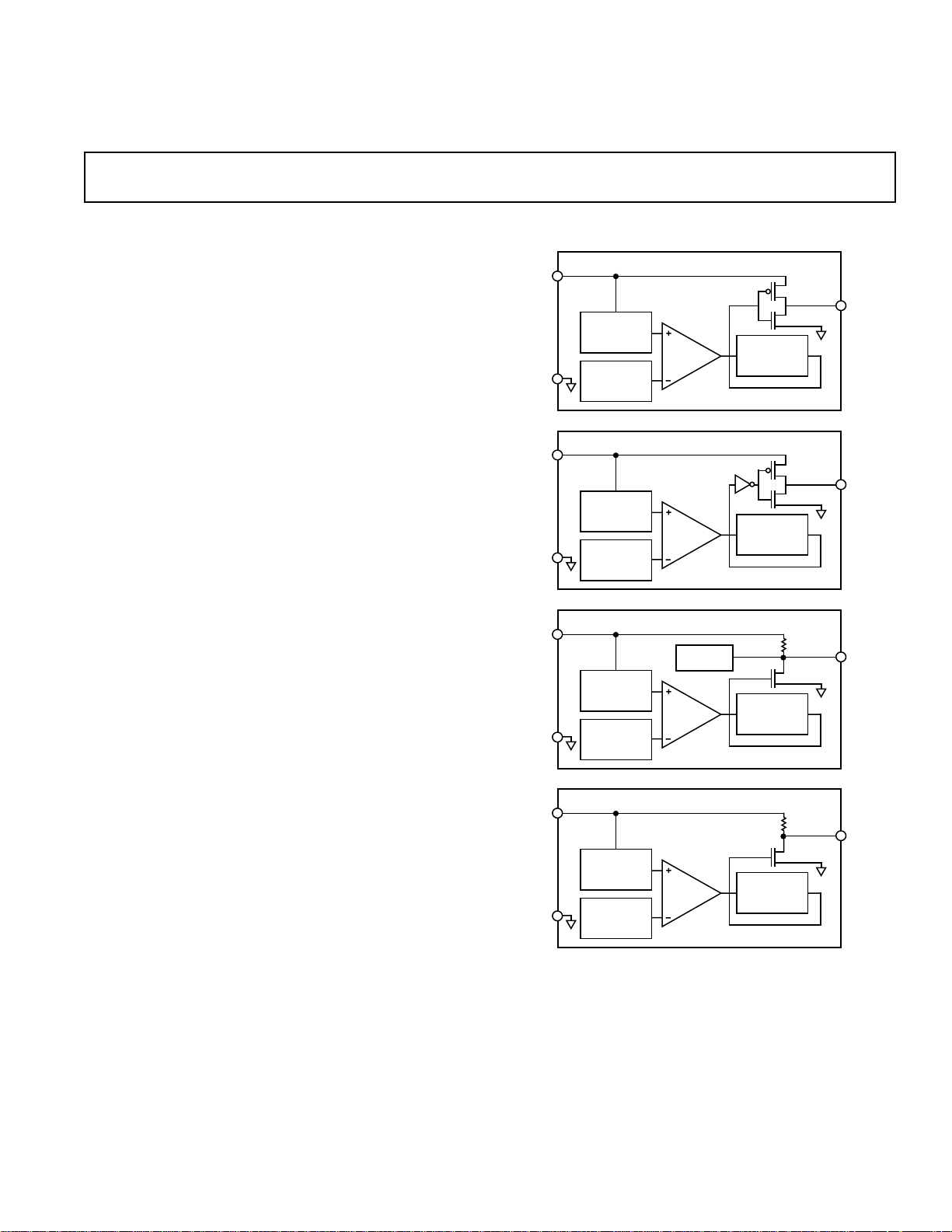
Microprocessor Reset Circuits
ADM1810–ADM1813/ADM1815–ADM1818
FEATURES
FUNCTIONAL BLOCK DIAGRAMS
Reliable Low Cost Voltage Monitor with Reset Output
Supports Monitoring of Supplies Within 5%, 10%, 15%
and 20% Tolerance
Active High and Low Push-Pull Output Choices
(ADM1810, ADM1812, ADM1815 and ADM1817)
Open Drain Output Choices (ADM1811, ADM1813,
ADM1816 and ADM1818)
Can Be Used with a Manual Push-Button to Generate a
Reset (ADM1813, ADM1818)
Initialize Microprocessor Systems with Added Safety
APPLICATIONS
Microprocessor Systems
Computers
Controllers
Intelligent Instruments
Automotive Systems
GENERAL DESCRIPTION
The ADM181x range of voltage monitoring circuits can be used
in any application where an electronic system needs to be reset
when a voltage increases above or below a predetermined value.
Because of the “reset delay time” incorporated into the ADM181x
series, these devices can provide a safe startup for electronic
systems. Before a system initializes, the power supply must stabilize. Using the ADM181x series ensures that there are typically
150 ms for the power supply to stabilize before the system is
reset and safe system initialization begins.
The ADM181x series of microprocessor reset circuits are available in low cost, space-saving SOT-23 packages.
One Technology Way, P.O. Box 9106, Norwood, MA 02062-9106, U.S.A.
Tel: 781/329-4700 World Wide Web Site: http://www.analog.com
Fax: 781/326-8703 © Analog Devices, Inc., 1999
REV. 0
Information furnished by Analog Devices is believed to be accurate and
reliable. However, no responsibility is assumed by Analog Devices for its
use, nor for any infringements of patents or other rights of third parties
which may result from its use. No license is granted by implication or
otherwise under any patent or patent rights of Analog Devices.
Page 2
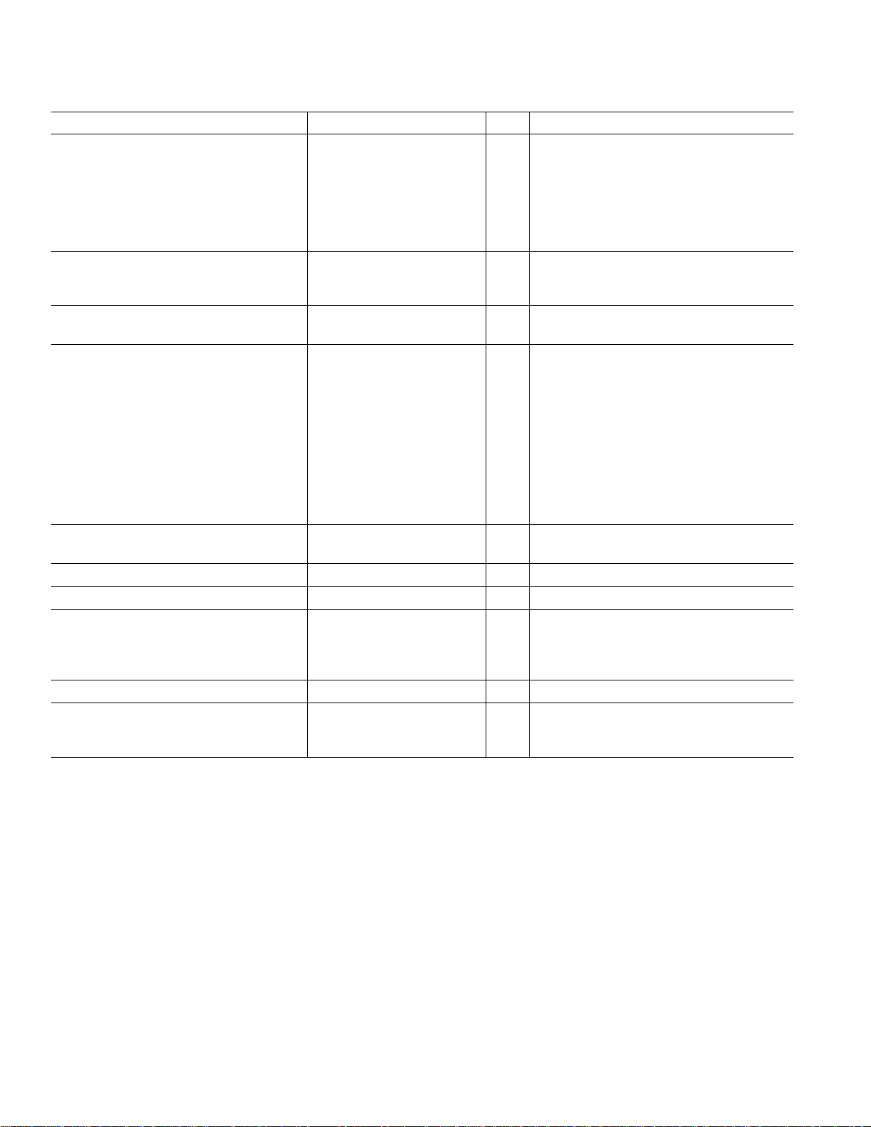
ADM1810–ADM1813/ADM1815–ADM1818–SPECIFICATIONS
(TA = –40ⴗC to +85ⴗC unless otherwise noted)
Parameter Min Typ Max Units Test Conditions/Note
SUPPLY
Voltage 1.2 5.5 V
Current 30 40 µA (ADM1810/ADM1811/ADM1813)
VCC < 5.5 V, RST Output Open
30 40 µA (ADM1812) V
28 35 µA (ADM1815/ADM1816/ADM1817/ADM1818)
VCC < 5.5 V, RST Output Open
OUTPUT CURRENT 8 mA @ 0.4 V, V
350 µA (ADM1810/ADM1812/ADM1815/ADM1817)
@ 2.4 V, V
OUTPUT VOLTAGE V
– 0.5 VCC – 0.1 V (ADM1810/ADM1812/ADM1815/ADM1817)
CC
@ 0 µA to 500 µA
V
TRIP-POINT
CC
ADM1810-5, ADM1810-10, ADM1810-15/
ADM1811/ADM1812/ADM1813-5 4.50 4.62 4.75 V (5%)
ADM1811/ADM1812/ADM1813-10 4.25 4.35 4.49 V (10%)
ADM1811/ADM1812/ADM1813-15 4.00 4.13 4.24 V (15%)
ADM1815/ADM1816/ADM1817/
ADM1818-5 2.98 3.06 3.15 V (5%)
ADM1815/ADM1816/ADM1817/
ADM1818-10 2.80 2.88 2.97 V (10%)
ADM1815/ADM1816/ADM1817/
ADM1818-20 2.47 2.55 2.64 V (20%)
INTERNAL PULL-UP RESISTOR
ADM1811/ADM1813/ADM1816/ADM1818 3.5 5.5 7.5 kΩ
OUTPUT CAPACITANCE 10 pF
RESET ACTIVE TIME 100 150 300 ms
V
DETECT TO RST
CC
Falling 5 10 µs (ADM1810/ADM1811/ADM1812/ADM1813)
715µs (ADM1815/ADM1816/ADM1817/ADM1818)
Rising 100 150 300 ms t
= 5 µs
R
PUSH-BUTTON DETECT TO RST 1 µs (ADM1813/ADM1818)
PUSH-BUTTON RESET
100 150 300 ms (ADM1818) 2.7 V ≤ VCC ≤ 3.3 V
100 150 300 ms (ADM1813)
NOTES
*For ADM181x-20, VCC = V
Specifications subject to change without notice.
, sink current reduces to 8 mA.
CCTP
CC
≥ 2.7 V*
CC
≥ 2.7 V
CC
< 5.5 V
–2–
REV. 0
Page 3

ADM1810–ADM1813/ADM1815–ADM1818
TOP VIEW
(Not to Scale)
RST/RST
V
CC
GND
ADM181x
1
2
3
V
CC
RST
V
CC
TRIP-POINT (MAX)
V
CC
TRIP-POINT
V
CC
TRIP-POINT (MIN)
RESET ACTIVE TIMEOUT
ORDERING GUIDE
Trip- Package Brand
Model* Point Option Information
ADM1810-5ART-REEL 4.62 V RT-3 (SOT-23) MZV
ADM1810-5ART-REEL7 4.62 V RT-3 (SOT-23) MZV
ADM1810-10ART-REEL 4.25 V RT-3 (SOT-23) MZT
ADM1810-10ART-RL7 4.25 V RT-3 (SOT-23) MZT
ADM1810-15ART-REEL 4.12 V RT-3 (SOT-23) MZQ
ADM1810-15ART-RL7 4.12 V RT-3 (SOT-23) MZQ
ADM1811-5ART-REEL 4.50 V RT-3 (SOT-23) M1V
ADM1811-5ART-RL7 4.50 V RT-3 (SOT-23) M1V
ADM1811-10ART-REEL 4.35 V RT-3 (SOT-23) M1T
ADM1811-10ART-RL7 4.35 V RT-3 (SOT-23) M1T
ADM1811-15ART-REEL 4.00 V RT-3 (SOT-23) M1Q
ADM1811-15ART-RL7 4.00 V RT-3 (SOT-23) M1Q
ADM1812-5ART-REEL 4.50 V RT-3 (SOT-23) MTV
ADM1812-5ART-RL7 4.50 V RT-3 (SOT-23) MTV
ADM1812-10ART-REEL 4.35 V RT-3 (SOT-23) MTT
ADM1812-10ART-RL7 4.35 V RT-3 (SOT-23) MTT
ADM1812-15ART-REEL 4.00 V RT-3 (SOT-23) MTQ
ADM1812-15ART-RL7 4.00 V RT-3 (SOT-23) MTQ
ADM1813-5ART-REEL 4.50 V RT-3 (SOT-23) M3V
ADM1813-5ART-RL7 4.50 V RT-3 (SOT-23) M3V
ADM1813-10ART-REEL 4.35 V RT-3 (SOT-23) M3T
ADM1813-10ART-RL7 4.35 V RT-3 (SOT-23) M3T
ADM1813-15ART-REEL 4.00 V RT-3 (SOT-23) M3Q
ADM1813-15ART-RL7 4.00 V RT-3 (SOT-23) M3Q
ADM1815-10ART-REEL 2.88 V RT-3 (SOT-23) M5E
ADM1815-10ART-RL7 2.88 V RT-3 (SOT-23) M5E
ADM1815-20ART-REEL 2.55 V RT-3 (SOT-23) M5A
ADM1815-20ART-RL7 2.55 V RT-3 (SOT-23) M5A
ADM1816-10ART-REEL 2.88 V RT-3 (SOT-23) M6E
ADM1816-10ART-RL7 2.88 V RT-3 (SOT-23) M6E
ADM1816-20ART-REEL 2.55 V RT-3 (SOT-23) M6A
ADM1816-20ART-RL7 2.55 V RT-3 (SOT-23) M6A
ADM1817-10ART-REEL 2.88 V RT-3 (SOT-23) M7E
ADM1817-10ART-RL7 2.88 V RT-3 (SOT-23) M7E
ADM1817-20ART-REEL 2.55 V RT-3 (SOT-23) M7A
ADM1817-20ART-RL7 2.55 V RT-3 (SOT-23) M7A
ADM1818-10ART-REEL 2.88 V RT-3 (SOT-23) M8E
ADM1818-10ART-RL7 2.88 V RT-3 (SOT-23) M8E
ADM1818-20ART-REEL 2.55 V RT-3 (SOT-23) M8A
ADM1818-20ART-RL7 2.55 V RT-3 (SOT-23) M8A
NOTES
RL7 or REEL7 are in reels of 3000 parts. REEL are in reels of 10000 parts.
All models in bold are ex-stock. Consult factory for availability.
*Only Available in Reels.
PIN CONFIGURATION
PIN FUNCTION DESCRIPTIONS
Pin Mnemonic Function
1 RST/RST Reset Output. RST/RST remains active while
VCC is below the reset threshold, and remains active for 150 ms (typ) after V
CC
rises
above the reset threshold.
2V
CC
Supply Voltage Being Monitored.
3 GND 0 V. Ground Reference for All Signals.
V
CC
VCC TRIP-POINT(MAX)
RST
TRIP-POINT
V
CC
V
TO RESET
CC
DELAY
VCC TRIP-POINT(MIN)
V
OL
Figure 1. Power-Down Timing Diagram
ABSOLUTE MAXIMUM RATINGS*
VCC . . . . . . . . . . . . . . . . . . . . . . . . . . . . . . . +1.2 V to +5.5 V
Input Current . . . . . . . . . . . . . . . . . . . . . . . . . . . . . . . . 40 µA
Operating Temperature Range . . . . . . . . . . . –40°C to +85°C
Power Dissipation, RT-3, SOT-23 . . . . . . . . . . . . . . 320 mW
Derate by 4 mW/°C Above +70°C
Thermal Impedance . . . . . . . . . . . . . . . . . . . . . . 333°C/W
θ
JA
Lead Temperature (Soldering, 10 sec) . . . . . . . . . . . +300°C
Vapor Phase (60 sec) . . . . . . . . . . . . . . . . . . . . . . . +215°C
Infrared (15 sec) . . . . . . . . . . . . . . . . . . . . . . . . . . . +220°C
Storage Temperature Range . . . . . . . . . . . . –65°C to +150°C
ESD Rating . . . . . . . . . . . . . . . . . . . . . . . . . . . . . . . . . . . 3 kV
*Typical values are measured at T
REV. 0
= +25°C unless otherwise noted.
A
Figure 2. Power-Up Timing Diagram
–3–
Page 4

ADM1810–ADM1813/ADM1815–ADM1818
ADM1813 AND ADM1818
The ADM1813 and ADM1818 are low cost voltage monitoring
devices with the inclusion of an optional push-button reset
function.
V
CC
ADM1813/
ADM1818
V
CC
RST
GND
MICRO-
PROCESSOR
RESET
Figure 3. ADM1813/ADM1818 Typical Application
An optional push-button reset switch can be connected between RST and ground. Pressing this switch will pull the reset
output low. If the push-button reset button pulls the RST
output low for a period greater than 1 µs, then, when the reset
button releases the RST line to float high, the RST line will
stay low for a further 150 ms typical.
VOLTAGE
INPUT LOW
PUSH-BUTTON TIME
RESET TIMEOUT
VOLTAGE
INPUT HIGH
Figure 4. Push-Button Reset Timing Diagram
The ADM1818 range has options which allow the user to
monitor 3.3 V supplies with 10% and 20% tolerance options.
While the ADM1813 range has options which allow the user
to monitor 5 V supplies with 5%, 10% and a 15% tolerance
options.
ADM1810, ADM1812, ADM1815 AND ADM1817
The ADM1812 is a 5 V low cost voltage monitor with an active
high push-pull output. The ADM1812 supports 5%, 10% and
15% tolerances. The ADM1810 is similar to the ADM1812,
except that the ADM1810 has an active low push-pull output.
The ADM1817 is 3.3 V voltage monitor with an active high
push-pull output. The ADM1817 supports 5%, 10% and 20%
tolerances. The ADM1815 is similar to the ADM1817, except
that the ADM1815 has an active low push-pull output.
The ADM1810/ADM1812/ADM1815/ADM1817 can be connected directly to most microprocessor-reset inputs without the
need for external components.
ADM1811 AND ADM1816
The ADM1811 is a low cost voltage monitor with an open drain
output. The ADM1811 is designed to monitor 5 V supplies.
The ADM1811 range comes in three different variants which
allow the monitoring of a 5 V supply with a tolerance of 5%,
10% and 15%. The ADM1816 is a 3.3 V version of the ADM1811
and supports 5%, 10% and 20% tolerance options.
V
CC
ADM1811/
ADM1816
V
CC
RST
GND
MICRO-
PROCESSOR
RESET
Figure 6. ADM1811/ADM1816 Typical Application
OUTLINE DIMENSIONS
Dimensions shown in inches and (mm).
3-Lead Plastic Surface Mount Package (SOT-23)
(RT-3)
0.1200 (3.048)
0.1102 (2.799)
0.0550 (1.397)
0.0470 (1.194)
PIN 1
0.0236 (0.599)
0.0177 (0.450)
0.0040 (0.102)
0.0005 (0.013)
SEATING
PLANE
3
1
0.0807 (2.050)
0.0701 (1.781)
0.0210 (0.533)
0.0146 (0.371)
0.1040 (2.642)
0.0827 (2.101)
2
0.0413 (1.049)
0.0374 (0.950)
0.0440 (1.118)
0.0320 (0.813)
0.0100 (0.254)
0.0050 (0.127)
0.0059 (0.150)
0.0034 (0.086)
0.027 (0.686)
REF
C3459–8–3/99
V
CC
ADM1810/
ADM1812/
ADM1815/
ADM1817
V
CC
RST/
RST
GND
MICRO-
PROCESSOR
RESET
Figure 5. ADM1810/ADM1812/ADM1815/ADM1817
Typical Application
–4–
PRINTED IN U.S.A.
REV. 0
 Loading...