

Page 1
www.BDTIC.com/ADI
Triple Processor Supervisors
FEATURES
Triple supervisory circuits
Supply voltage range of 2.0 V to 5.5 V
Pretrimmed threshold options: 1.8 V, 2.5 V, 3.3 V, and 5 V
Adjustable 0.6 V and 1.25 V voltage references
Maximum supply current of 40 μA
140 ms (minimum) reset timeout
RESET valid from V
Push-pull RESET and
8-lead, narrow body SOIC package
Temperature range: −40°C to +85°C
APPLICATIONS
Supervising DSPs/microcontrollers
Industrial and portable equipment
Wireless systems
Notebook/desktop computers
GENERAL DESCRIPTION
The ADM13307 is a triple voltage supervisor designed to
monitor up to three voltage levels in DSP and microprocessorbased systems.
There are five models available, all of which feature a combination of internally pretrimmed undervoltage threshold options
for monitoring 1.8 V, 2.5 V, 3.3 V, and 5 V supplies. There are
also two adjustable input options with undervoltage thresholds of
either 0.6 V or 1.25 V.
The ADM13307-18, ADM13307-25, and ADM13307-33
models have two internally fixed thresholds and one externally
programmable threshold via a resistor string. The ADM13307-4
and ADM13307-5 offer one internally fixed threshold and two
externally programmable thresholds. See the Ordering Guide
for a list of all available options.
During power-up,
exceeds 1.1 V. The device then monitors the SENSEv input
pins and holds the
pins remain below the rising threshold voltage, V
Once the supplies monitored at the SENSEv inputs rise above
their associated thresholds, the reset signal remains low for the
reset timeout period before deasserting. Subsequently, if a voltage monitored by the SENSEv pins falls below its associated
falling input threshold voltage, V
≥ 1.1 V
DD
outputs
RESET
is asserted when the supply voltage
RESET
output low as long as the SENSEv
RESET
, the
RESET
IT−
.
IT+
output asserts.
ADM13307
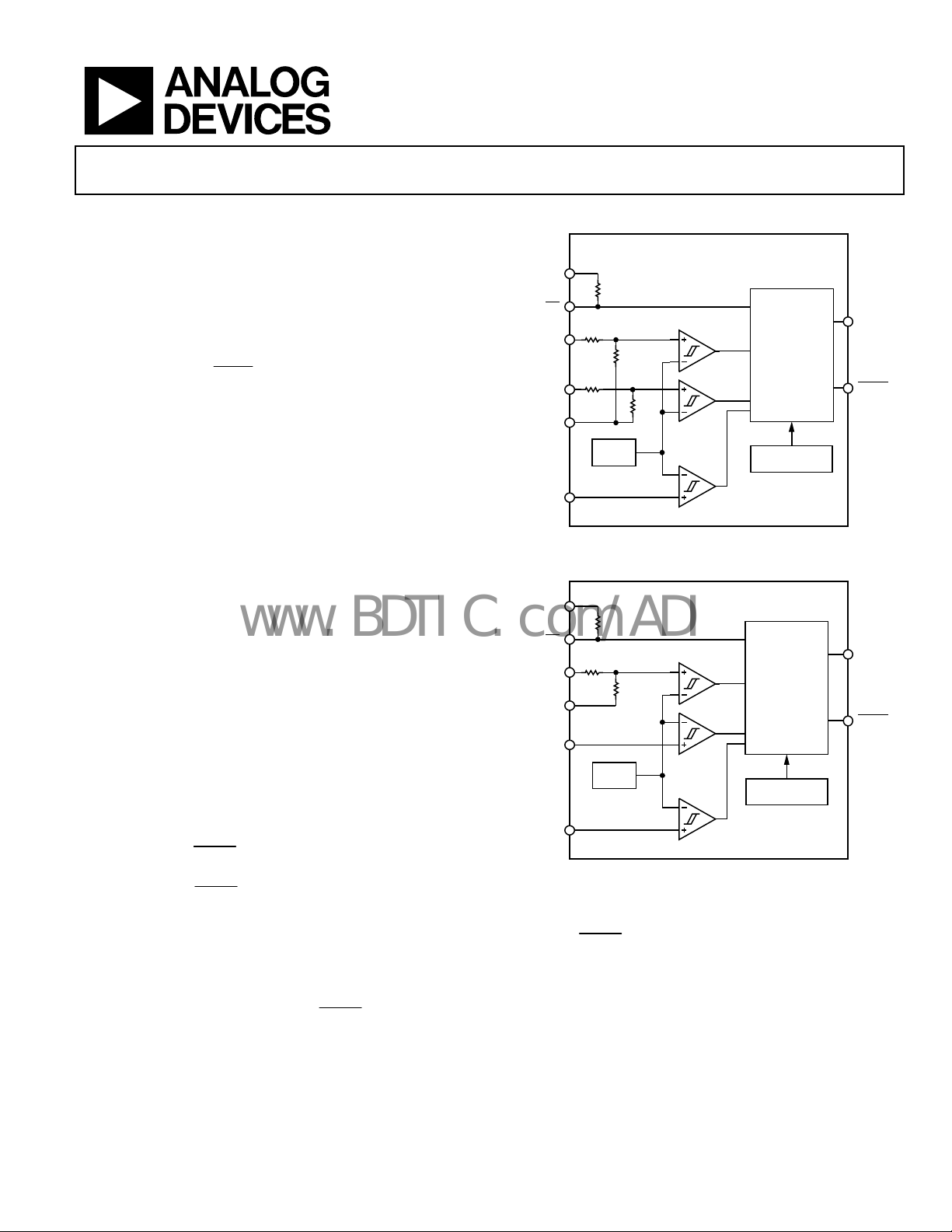
FUNCTIONAL BLOCK DIAGRAMS
ADM13307-18
V
DD
14kΩ
MR
SENSE1
SENSE2
GND
SENSE3
R1
R2
R3
R4
1.25V
Figure 1.
V
DD
14kΩ
MR
SENSE1
GND
SENSE2
SENSE3
R1
R2
0.6V
Figure 2.
The ADM13307 features both an active high RESET and an
active low
RESET
output.
The manual reset input of the ADM13307 can be used to initiate
a reset by means of an external push button or logic signal.
The ADM13307 is available in an 8-lead narrow body SOIC
package. The device operates over the extended industrial
temperature range of −40°C to +85°C.
ADM13307-25
ADM13307-33
RESET
LOGIC + TIMER
OSCIL LATO R
ADM13307-4
ADM13307-5
RESET
LOGIC + TIMER
OSCILLATOR
RESET
RESET
RESET
RESET
06923-002
06923-001
Rev. 0
Information furnished by Analog Devices is believed to be accurate and reliable. However, no
responsibility is assumed by Analog Devices for its use, nor for any infringements of patents or other
rights of third parties that may result from its use. Specifications subject to change without notice. No
license is granted by implication or otherwise under any patent or patent rights of Analog Devices.
Trademarks and registered trademarks are the property of their respective owners.
One Technology Way, P.O. Box 9106, Norwood, MA 02062-9106, U.S.A.
Tel: 781.329.4700 www.analog.com
Fax: 781.461.3113 ©2007 Analog Devices, Inc. All rights reserved.
Page 2

ADM13307
www.BDTIC.com/ADI
TABLE OF CONTENTS
Features .............................................................................................. 1
Applications ....................................................................................... 1
General Description ......................................................................... 1
Functional Block Diagrams ............................................................. 1
Revision History ............................................................................... 2
Specifications ..................................................................................... 3
Timing Requirements .................................................................. 5
Switching Characteristics ............................................................ 5
Functional Truth Table ................................................................ 5
Absolute Maximum Ratings ............................................................ 6
REVISION HISTORY
8/07—Revision 0: Initial Version
Thermal Resistance .......................................................................6
ESD Caution...................................................................................6
Pin Configuration and Function Descriptions ..............................7
Typical Performance Characteristics ..............................................8
Theory of Operation ...................................................................... 10
Input Configuration ................................................................... 10
Reset Output ............................................................................... 10
Manual Reset (MR) .................................................................... 10
Outline Dimensions ....................................................................... 11
Ordering Guide .......................................................................... 11
Rev. 0 | Page 2 of 12
Page 3
ADM13307
www.BDTIC.com/ADI
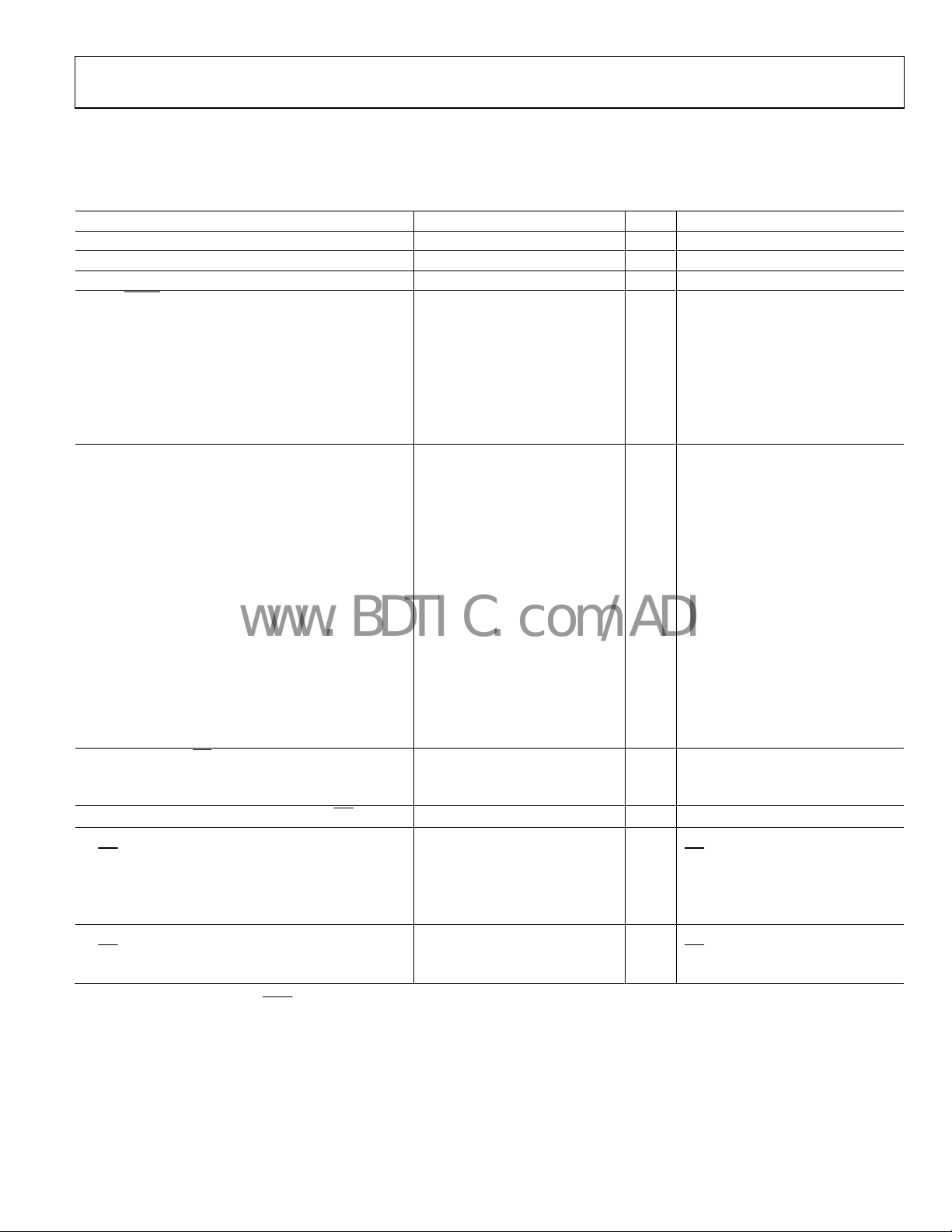
SPECIFICATIONS
VDD = 2.0 V to 5.5 V, −40°C ≤ TA ≤ +85°C, unless otherwise noted.
Table 1. ADM13307-18, ADM13307-25, and ADM13307-33
Parameter Min Typ Max Unit Test Conditions/Comments
OPERATING VOLTAGE RANGE, VDD 2.0 5.5 V
SUPPLY CURRENT, I
INPUT CAPACITANCE, CI 10 pF VI = 0 V to VDD
RESET, RESET Output
High Level Output Voltage, VOH V
V
V
Low Level Output Voltage, VOL 0.2 V IOL = 20 μA
0.4 V IOL = 2 mA, VDD = 3.3 V
0.4 V IOL = 3 mA, VDD = 5.5 V
Power-Up Reset Voltage1 0.4 V IOL = 20 μA, VDD ≥ 1.1 V
SENSE INPUTS
Falling Input Threshold Voltage, V
1.64 1.68 1.72 V TA = 0°C to 85°C
2.20 2.25 2.30 V TA = 0°C to 85°C
2.86 2.93 3.00 V TA = 0°C to 85°C
4.46 4.55 4.64 V TA = 0°C to 85°C
1.22 1.25 1.29 V TA = −40°C to +85°C
1.64 1.68 1.73 V TA = −40°C to +85°C
2.20 2.25 2.32 V TA = −40°C to +85°C
2.86 2.93 3.02 V TA = −40°C to +85°C
4.46 4.55 4.67 V TA = −40°C to +85°C
Hysteresis at SENSEv Inputs, V
15 mV V
20 mV V
30 mV V
40 mV V
INPUT VOLTAGE AT MR
High Level, VIH
Low Level, VIL
INPUT TRANSITION RISE AND FALL RATE AT MR
HIGH LEVEL INPUT CURRENT, I
MR
SENSE1 5 8 μA SENSE1 = VDD = 5.5 V
SENSE2 6 9 μA SENSE2 = VDD = 5.5 V
SENSE3 −25 +25 nA SENSE3 = VDD
LOW LEVEL INPUT CURRENT, IL
MR
SENSEv −25 +25 nA SENSE1, SENSE2, SENSE3 = 0 V
1
The lowest supply voltage at which
40 μA
DD
− 0.2 V IOH = −20 μA
DD
− 0.4 V IOH = −2 mA, VDD = 3.3 V
DD
− 0.4 V IOH = −3 mA, VDD = 5.5 V
DD
1.22 1.25 1.28 V TA = 0°C to 85°C
IT−
10 mV V
HYS
0.7 × V
0.3 × V
V
DD
V
DD
= 1.25 V
IT−
= 1.68 V
IT−
= 2.25 V
IT−
= 2.93 V
IT−
= 4.55 V
IT−
50 ns/V
H
RESET
becomes active. tr, VDD ≥ 15 μs/V.
−130 −180 μA
−430 −600 μA
MR = 0.7 × VDD, VDD = 5.5 V
MR = 0 V, VDD = 5.5 V
Rev. 0 | Page 3 of 12
Page 4
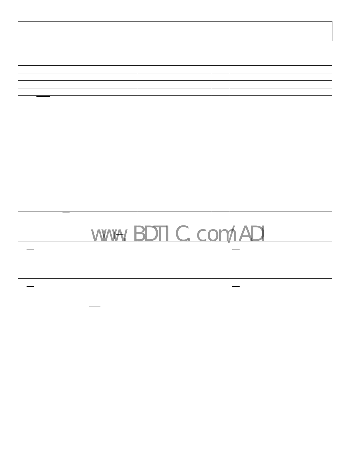
ADM13307
www.BDTIC.com/ADI
VDD = 2.0 V to 5.5 V, −40°C ≤ TA ≤ +85°C, unless otherwise noted.
Table 2. ADM13307-4 and ADM13307-5
Parameter Min Typ Max Unit Test Conditions/Comments
OPERATING VOLTAGE RANGE, VDD 2.0 5.5 V
SUPPLY CURRENT, I
INPUT CAPACITANCE, CI 10 pF VI = 0 V to VDD
RESET, RESET Output
High Level Output Voltage, VOH V
V
V
Low Level Output Voltage, VOL 0.2 V IOL = 20 μA
0.4 V IOL = 2 mA, VDD = 3.3 V
0.4 V IOL = 3 mA, VDD = 5.5 V
Power-Up Reset Voltage
SENSE INPUTS
Falling Input Threshold Voltage, V
0.5952 0.6 0.6048 V TA = −40°C to +85°C, 2.35 V ≤ VDD ≤ 5.5 V
2.23 2.25 2.29 V TA = −40°C to +85°C
2.90 2.93 2.98 V TA = −40°C to +85°C
Hysteresis at SENSEv Inputs, V
20 mV V
30 mV V
INPUT VOLTAGE AT MR
High Level, V
Low Level, V
INPUT TRANSITION RISE AND FALL RATE AT MR
HIGH LEVEL INPUT CURRENT, IH
MR
SENSE1 5 8 μA SENSE1 = VDD = 5.5 V
SENSE2 −50 +50 nA SENSE2 = VDD = 5.5 V
SENSE3 −25 +25 nA SENSE3 = VDD
LOW LEVEL INPUT CURRENT, IL
MR
SENSEv −25 +25 nA SENSE1, SENSE2, SENSE3 = 0 V
1
The lowest supply voltage at which
40 μA
DD
− 0.2 V IOH = −20 μA
DD
− 0.4 V IOH = −2 mA, VDD = 3.3 V
DD
− 0.4 V IOH = −3 mA, VDD = 5.5 V
DD
1
0.5946 0.6 0.6048 V TA = −40°C to +85°C
IT−
0 mV V
HYS
IH
IL
0.4 V IOL = 20 μA, VDD ≥ 1.1 V
= 0.6 V
IT−
= 2.25 V
IT−
= 2.93 V
IT−
0.7 × VDD V
0.3 × VDD V
50 ns/V
RESET
becomes active. tr, VDD ≥ 15 μs/V.
−130 −180 μA
−430 −600 μA
= 0.7 × VDD, VDD = 5.5 V
MR
= 0 V, VDD = 5.5 V
MR
Rev. 0 | Page 4 of 12
Page 5

ADM13307
www.BDTIC.com/ADI
TIMING REQUIREMENTS
VDD = 2.0 V to 5.5 V, RL = 1 MΩ, CL = 50 pF, TA = 25°C.
Table 3. ADM13307-18, ADM13307-25 and ADM13307-33
Parameter Min Typ Max Unit Test Conditions/Comments
Pulse Width (tw)
SENSEv 6 μs V
MR
100 ns VIH = 0.7 × VDD, VIL = 0.3 × VDD
Table 4. ADM13307-4 and ADM13307-5
Parameter Min Typ Max Unit Test Conditions/Comments
Pulse Width (tw)
SENSEv 30 μs V
MR
100 ns VIH = 0.7 × VDD, VIL = 0.3 × VDD
SWITCHING CHARACTERISTICS
VDD = 2.0 V to 5.5 V, RL = 1 MΩ, CL = 50 pF, TA = 25°C
Table 5. ADM13307-18, ADM13307-25 and ADM13307-33
Parameter Min Typ Max Unit Test Conditions/Comments
Delay Time (td) 140 200 280 ms
Propagation Delay, High-to-Low, MR to RESET1/RESET (t
Propagation Delay, Low-to-High, MR to RESET/RESET1 (t
Propagation Delay, High-to-Low, SENSEv to RESET1/RESET (t
Propagation Delay, Low-to-High, SENSEv to RESET/RESET1 (t
1
The reset timeout delay of 200 ms masks the propagation delay
200 500 ns V
)
PHL
200 500 ns V
)
PLH
1 5 μs
)
PHL
1 5 μs
)
PLH
SENSEvL
SENSEvL
= V
= V
− 0.3 V, V
IT−
− 0.3 V, V
IT−
V
I(SENSEv)
I(SENSEv)
I(SENSEv)
VIH = V
VIH = V
= V
SENSEvH
SENSEvH
≥ V
+ 0.2 V, MR ≥ 0.7 × VDD
IT+
≥ V
+ 0.2 V, VIH ≥ 0.7 × VDD, VIL ≥ 0.3 × VDD
IT+
≥ V
+ 0.2 V, VIH ≥ 0.7 × VDD, VIL ≥ 0.3 × VDD
IT+
+ 0.3 V, VIL = V
IT+
+ 0.3 V, VIL = V
IT+
+ 0.3 V
IT+
= V
+ 0.3 V
IT+
− 0.3 V, MR ≥ 0.7 × VDD
IT−
− 0.3 V, MR ≥ 0.7 × VDD
IT−
Table 6. ADM13307-4 and ADM13307-5
Parameter Min Typ Max Unit Test Conditions/Comments
Delay Time (td) 140 200 280 ms
Propagation Delay, High-to-Low, MR to RESET1/RESET (t
Propagation Delay, Low-to-High, MR to RESET/RESET1 (t
Propagation Delay, High-to-Low, SENSEv to RESET1/RESET (t
Propagation Delay, Low-to-High, SENSEv to RESET/RESET1 (t
1
The reset timeout delay of 200 ms masks the propagation delay.
200 500 ns V
)
PHL
200 500 ns V
)
PLH
30 μs
)
PHL
30 μs
)
PLH
V
I(SENSEv)
I(SENSEv)
I(SENSEv)
VIH = V
VIH = V
≥ V
+ 0.2 V, MR ≥ 0.7 × VDD
IT+
≥ V
+ 0.2 V, VIH ≥ 0.7 × VDD, VIL ≥ 0.3 × VDD
IT+
≥ V
+ 0.2 V, VIH ≥ 0.7 × VDD, VIL ≥ 0.3 × VDD
IT+
+ 0.3 V, VIL = V
IT+
+ 0.3 V, VIL = V
IT+
− 0.3 V, MR ≥ 0.7 × VDD
IT−
− 0.3 V, MR ≥ 0.7 × VDD
IT−
FUNCTIONAL TRUTH TABLE
Table 7.
SENSE1 > V
MR
L X1 X
H 0 0 0 L H
H 0 0 1 L H
H 0 1 0 L H
H 0 1 1 L H
H 1 0 0 L H
H 1 0 1 L H
H 1 1 0 L H
H 1 1 1 H L
1
X = don’t care.
SENSE2 > V
IT1
1
X
SENSE3 > V
IT2
1
L H
IT3
RESET
RESET
Rev. 0 | Page 5 of 12
Page 6

ADM13307
www.BDTIC.com/ADI
ABSOLUTE MAXIMUM RATINGS
Table 8.
Parameter Rating
Supply Voltage Range, VDD −0.3 V to +6 V
MR
SENSE1, SENSE2, SENSE3 (VDD + 0.3 V)VIT/V
RESET, RESET
Maximum Low Output Current 5 mA
Maximum High Output Current −5 mA
Input Clamp Current (VI < 0 V, VI > VDD) ±20 mA
Output Clamp Current (VO < 0 V, VO > VDD) ±20 mA
Operating Temperature Range −40°C to +85°C
Storage Temperature Range −65°C to +150°C
Lead Temperature
Soldering (10 sec) 300°C
Vapor Phase (60 sec) 215°C
Infrared (15 sec) 220°C
−0.3 V to V
−0.3 V to +6 V
+ 0.3 V
DD
REF
Stresses above those listed under Absolute Maximum Ratings
may cause permanent damage to the device. This is a stress
rating only; functional operation of the device at these or any
other conditions above those indicated in the operational
section of this specification is not implied. Exposure to absolute
maximum rating conditions for extended periods may affect
device reliability.
THERMAL RESISTANCE
Table 9.
Package Type θJA Unit
8-Lead SOIC_N (R-8) 206 °C/W
ESD CAUTION
Rev. 0 | Page 6 of 12
Page 7

ADM13307
www.BDTIC.com/ADI
PIN CONFIGURATION AND FUNCTION DESCRIPTIONS
1
SENSE1
SENSE2 2
SENSE3 3
ADM13307
TOP VIEW
(Not to Scale)
GND 4
Figure 3.Pin Configuration
8
V
DD
MR7
RESET6
RESET5
06923-003
Table 10. Pin Function Descriptions
Pin No. Mnemonic Description
1 SENSE1 Sense Voltage Input 1.
2 SENSE2 Sense Voltage Input 2.
3 SENSE3 Sense Voltage Input 3.
4 GND Ground.
5
RESET
Active Low Reset Output.
6 RESET Active High Reset Output.
7
MR
Manual Reset.
8 VDD Supply Voltage.
Rev. 0 | Page 7 of 12
Page 8

ADM13307
www.BDTIC.com/ADI
TYPICAL PERFORMANCE CHARACTERISTICS
0.6003
0.6001
(V)
IT
0.5999
0.5997
0.5995
0.5993
0.5991
0.5989
INPUT THRESHOLD VOLTAGE, V
0.5987
0.5985
–40–200 20406080
FREE AIR TEM PERATURE, TA (°C)
TA = 25°C
V
= 2V
DD
MR = OPEN
Figure 4. Sense Threshold Voltage vs. Free Air Temperature at V
40
35
30
(µA)
25
DD
20
15
10
5
SUPPLY CURRENT, I
–5
–10
0
–1.0
–0.500.5
1.0
2.0
2.5
3.0
1.5
SUPPLY VOLTAGE, VDD (V)
3.5
SENSEv = 5.5V
MR = OPEN
T
4.0
4.5
= 25°C
A
5.0
5.5
6.0
Figure 5. Supply Current vs. Supply Voltage Figure 8. ADM13307-4 and ADM13307-5 Minimum Pulse Duration at Sense
DD
6.5
10
(µs)
9
W
t
8
7
6
5
4
3
2
1
06923-004
MINIMUM PUL SE DURATION AT SENSE,
0
01
100 200 300 400 500 600 700 800 900
SENSE THRESHOLD OVERDRIVE (mV)
Figure 7. ADM13307-18, ADM13307-25 and ADM13307-33 Minimum Pulse
VDD = 5.5V
MR = OPEN
06923-007
000
Duration at Sense vs. Sense Threshold Overdrive
40
(µs)
39
W
38
37
36
35
34
33
32
31
06923-005
MINIMUM PUL SE DURATION AT SENSE, t
30
0 1000
100 200 300 400 500 600 700 800 900
SENSE THRESHOLD OVERDRIVE (mV)
VDD = 5.5V
MR = OPEN
06923-017
vs. Sense Threshold Overdrive
200
100
0
–100
(µA)
I
–200
–300
–400
–500
INPUT CURRENT, I
–600
–700
–800
–900
–1.0 7.0
–0.500.5
1.0
2.0
3.0
1.5
2.5
INPUT VOLTAGE AT MR, VI (V)
3.5
4.0
4.5
VDD = 5.5V
T
5.0
5.5
= 25°C
A
6.0
06923-006
6.5
Figure 6. Input Current vs. Input Voltage at MR
Rev. 0 | Page 8 of 12
2.50
(V)
OH
2.00
1.50
1.00
0.50
HIGH LEVEL OUTPUT VOLTAGE, V
VDD = 2V
MR = OPEN
0
0––5–4–3–2–1
HIGH LEVEL OUTPUT CURRENT, IOH (mA)
–40°C
0°C
+25°C
+85°C
Figure 9. High Level Output Voltage vs. High Level Output Current
06923-008
6
Page 9

ADM13307
www.BDTIC.com/ADI
6.0
5.5
(V)
5.0
OH
4.5
4.0
3.5
3.0
2.5
2.0
1.5
1.0
HIGH LEVEL OUTPUT VOLTAGE, V
0.5
0
VDD = 5.5V
MR = OPEN
0––50–40–30–20–10
HIGH LEVEL OUTPUT CURRENT, I
OH
(mA)
–40°C
0°C
+25°C
+85°C
60
Figure 10. High Level Output Voltage vs. High Level Output Current
06923-009
1.0
0.9
(V)
OL
0.8
0.7
0.6
0.5
0.4
0.3
0.2
LOW LEVEL OUTPUT VOLTAGE, V
0.1
–40°C
0°C
+25°C
+85°C
VDD = 5.5V
0
06
5 10152025303540455055
LOW LE VEL OUTPUT CURRENT, IOL (mA)
MR = OPEN
06923-016
0
Figure 12. Low Level Output Voltage vs. Low Level Output Current
0.25
(V)
OL
0.20
0.15
0.10
0.05
LOW LEVEL OUTPUT VOLTAGE, V
–40°C
0°C
+25°C
+85°C
0
06
24135
LOW LE VEL OUTPUT CURRENT, IOL (mA)
Figure 11. Low Level Output Voltage vs. Low Level Output Current
VDD = 2V
MR = OPEN
06923-010
Rev. 0 | Page 9 of 12
Page 10

ADM13307
www.BDTIC.com/ADI
THEORY OF OPERATION
The ADM13307 devices are triple voltage supervisors designed
to monitor up to three supplies and provide a reset signal to
DSP and microprocessor-based systems.
There are five models available, all of which feature a combination of internally pretrimmed undervoltage threshold options
for monitoring 1.8 V, 2.5 V, 3.3 V, and 5 V supplies. There are
also adjustable input options with threshold voltages of either
0.6 V or 1.25 V.
ADM13307-18, ADM13307-25, and ADM13307-33 models
have two internally fixed thresholds and one externally
programmable threshold, via a resistor string, while the
ADM13307-4 and ADM13307-5 offer one internally fixed
threshold and two externally programmable thresholds via a
resistor string. See the Ordering Guide for a list of all available
options.
INPUT CONFIGURATION
The ADM13307 is powered through VDD. To increase noise
immunity in noisy applications, place a 0.1 μF capacitor
between the V
The SENSEv inputs are resistant to short power supply glitches.
Do not allow unused SENSEv inputs to float or to be grounded,
instead connect it to a supply voltage greater than its specified
threshold voltage.
Typically, the threshold voltage at an adjustable SENSEv input
is either 0.6 V or 1.25 V. Refer to the Ordering Guide for details.
For example, to monitor a voltage greater than 1.25 V, connect a resistor divider network to the device as depicted in
Figure 13, where,
V
MONITERED
input and ground.
DD
+
R2R1
R2
V
⎞
⎟
⎠
REF
= 1.25V
=
Figure 13. Setting the Adjustable Monitor
⎜
⎝
MONITORED VOLTAGE
R1
R2
⎛
V25.1
06923-012
RESET OUTPUT
The reset outputs are guaranteed to be in the correct state for
down to 1.1 V. During power up,
V
DD
RESET
is asserted when
the supply voltage becomes greater than 1.1 V.
Once the supplies monitored at the SENSEv pins rise above their
RESET
associated threshold level, the
signal remains low for the
reset timeout period before deasserting. Subsequently, if a supply
monitored by the SENSEv pins falls below its associated thresh-
RESET
old, the
SENSEv
V
(NOM)
V
IT–
RESET
1
0
The ADM13307 features both an active-low push-pull
output reasserts.
t
d
Figure 14. Reset Timing Diagram
t
t
t
d
RESET
output and active-high push-pull RESET output.
MANUAL RESET (MR)
The ADM13307 features a manual reset input, which when driven
low, asserts the reset output, as shown in Figure 15. When
transitions from low to high, the reset remains asserted for the
duration of the reset active timeout period before deasserting.
An external push-button switch can be connected between
and ground to allow the user to generate a reset.
MR
1
0
RESET
1
0
t
d
Figure 15. Manual Reset Timing Diagram
MR
MR
t
t
06923-015
06923-013
Rev. 0 | Page 10 of 12
Page 11

ADM13307
www.BDTIC.com/ADI
OUTLINE DIMENSIONS
5.00 (0.1968)
4.80 (0.1890)
4.00 (0.1574)
3.80 (0.1497)
0.25 (0.0098)
0.10 (0.0040)
COPLANARITY
0.10
CONTROLL ING DIMENSI ONS ARE IN MILLIMETERS; INCH DI MENSIONS
(IN PARENTHESES) ARE ROUNDED-OFF MILLIMETER EQUIVALENTS FOR
REFERENCE ONLY AND ARE NOT APPROPRI ATE FOR USE IN DESIGN.
85
1
4
1.27 (0.0500)
BSC
0.51 (0.0201)
SEATING
PLANE
COMPLIANT TO JEDEC STANDARDS MS-012-A A
0.31 (0.0122)
Figure 16. 8-Lead Standard Small Outline Package [SOIC_N]
Dimensions shown in millimeters and (inches).
ORDERING GUIDE
Nominal Input Voltage Threshold Voltage (Typical)
Model
ADM13307-18ARZ
1
ADM13307-18ARZ-RL7
ADM13307-25ARZ
1
ADM13307-25ARZ-RL7
ADM13307-33ARZ
1
ADM13307-33ARZ-RL7
1
ADM13307-4ARZ
ADM13307-4ARZ-RL7
1
ADM13307-5ARZ
ADM13307-5ARZ-RL7
1
Z = RoHS Compliant Part.
2
1.25 V adjustable. External resistor divider determines the actual sense voltage.
3
0.6 V adjustable. External resistor divider determines the actual sense voltage.
SENSE1 SENSE2 SENSE3 SENSE1 SENSE2 SENSE3
Adj
Adj
Adj
Adj
Adj
Adj
Adj
Adj
Adj
2
2.93 V 1.68 V 1.25 V –40°C to +85°C 8-Lead SOIC_N R-8
2
2.93 V 1.68 V 1.25 V –40°C to +85°C 8-Lead SOIC_N R-8
2
2.93 V 2.25 V 1.25 V –40°C to +85°C 8-Lead SOIC_N R-8
2
2.93 V 2.25 V 1.25 V –40°C to +85°C 8-Lead SOIC_N R-8
2
4.55 V 2.93 V 1.25 V –40°C to +85°C 8-Lead SOIC_N R-8
2
4.55 V 2.93 V 1.25 V –40°C to +85°C 8-Lead SOIC_N R-8
3
2.25 V 0.6 V 0.6 V –40°C to +85°C 8-Lead SOIC_N R-8
3
2.25 V 0.6 V 0.6 V –40°C to +85°C 8-Lead SOIC_N R-8
3
2.93 V 0.6 V 0.6 V –40°C to +85°C 8-Lead SOIC_N R-8
3
2.93 V 0.6 V 0.6 V –40°C to +85°C 8-Lead SOIC_N R-8
3.3 V 1.8 V Adj
1
3.3 V 1.8 V
3.3 V 2.5 V
1
3.3 V 2.5 V
5 V 3.3 V
1
5 V 3.3 V
2.5 V Adj
1
2.5 V
3.3 V
1
3.3 V
Adj
Adj
Adj
3
3
3
3
6.20 (0.2441)
5.80 (0.2284)
1.75 (0.0688)
1.35 (0.0532)
Narrow Body
(R-8)
8°
0°
0.25 (0.0098)
0.17 (0.0067)
0.50 (0.0196)
0.25 (0.0099)
1.27 (0.0500)
0.40 (0.0157)
Temperature
Range
45°
012407-A
Package
Description
Package
Option
Rev. 0 | Page 11 of 12
Page 12

ADM13307
www.BDTIC.com/ADI
NOTES
©2007 Analog Devices, Inc. All rights reserved. Trademarks and
registered trademarks are the property of their respective owners.
D06923-0-8/07(0)
Rev. 0 | Page 12 of 12
 Loading...