

Page 1
±0.8% Accurate Quad UV/OV
V
Positive/Negative Voltage Supervisor
FEATURES
Quad undervoltage/overvoltage (UV/OV) positive/negative
supervisor
Supervises up to two negative rails
Adjustable UV and OV input thresholds
Industry leading threshold accuracy over the extended
temperature range: ±0.8%
1 V buffered reference output
Open-drain
Adjustable reset timeout with disable option
Outputs guaranteed down to V
Glitch immunity
62 μA supply current
16-lead QSOP package
Specified from −40°C to +125°C
APPLICATIONS
Server supply monitoring
FPGA/DSP core and I/O voltage monitoring
Telecommunications equipment
Medical equipment
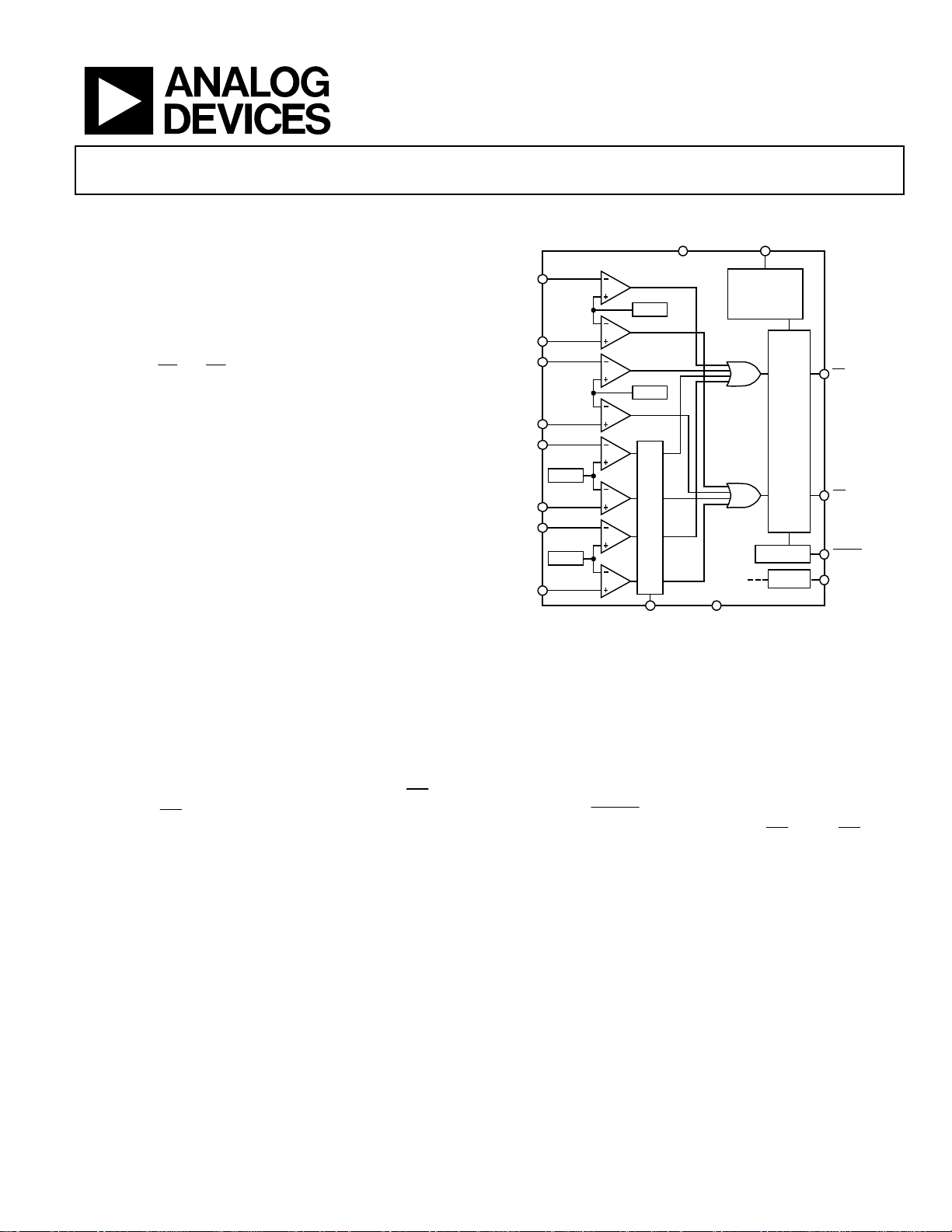
GENERAL DESCRIPTION
The ADM12914 is a quad voltage supervisory IC ideally suited
for monitoring multiple rails in a wide range of applications.
Each monitored rail has two dedicated input pins, VHx and VLx,
which allows each rail to be monitored for both undervoltage
(UV) and overvoltage (OV) conditions with high threshold
accuracy of ±0.8%. Common active low undervoltage (
overvoltage (
voltage rails.
The ADM12914 includes a 1 V buffered reference output, REF,
that acts as an offset when monitoring a negative voltage. The
three-state SEL pin determines the polarity of the third and
fourth inputs, that is, it configures the device to monitor
positive or negative supplies.
The device incorporates an internal shunt regulator that enables
the device to be used in higher voltage systems. This feature
UV
and OV reset outputs
of 0.9 V
CC
OV
) pins are shared by each of the monitored
UV
) and
ADM12914
FUNCTIONAL BLOCK DIAGRAM
CC
ADM12914
VH1
500mV
VL1
VH2
500mV
VL2
VH3
500mV
VL3
VH4
500mV
VL4
MUX
SEL GND
Figure 1.
requires a resistor to be placed between the main supply rail and
the V
pin to limit the current flow into the VCC pin at a level
CC
no greater than 10 mA. The ADM12914 uses the internal shunt
regulator to regulate V
if the supply line exceeds the absolute
CC
maximum ratings.
The ADM12914 is available in two models. The ADM12914-1
offers a latching overvoltage output that can be cleared by
toggling the
LATCH
input pin. The ADM12914-2 has a disable
pin that can override and disable both the
output signals.
The ADM12914 is available in a 16-lead QSOP package. The
device is specified over the extended temperature range of
−40°C to +125°C.
TIMER
TIMER
UV
OUTPUT
LOGIC
LOGIC
REF
and the
UV
OV
LATCH/DIS
REF
OV
08265-001
Rev. C
Information furnished by Analog Devices is believed to be accurate and reliable. However, no
responsibility is assumed by Analog Devices for its use, nor for any infringements of patents or other
rights of third parties that may result from its use. Specifications subject to change without notice. No
license is granted by implication or otherwise under any patent or patent rights of Analog Devices.
Trademarks and registered trademarks are the property of their respective owners.
One Technology Way, P.O. Box 9106, Norwood, MA 02062-9106, U.S.A.
Tel: 781.329.4700 www.analog.com
Fax: 781.461.3113 ©2009-2010 Analog Devices, Inc. All rights reserved.
Page 2

ADM12914
TABLE OF CONTENTS
Features .............................................................................................. 1
Applications ....................................................................................... 1
Functional Block Diagram .............................................................. 1
General Description ......................................................................... 1
Revision History ............................................................................... 2
Specifications ..................................................................................... 3
Absolute Maximum Ratings ............................................................ 4
ESD Caution .................................................................................. 4
Pin Configurations and Function Descriptions ........................... 5
Typical Performance Characteristics ............................................. 7
Theory of Operation ........................................................................ 9
Voltage Supervision ...................................................................... 9
Polarity Configuration ................................................................. 9
Monitoring Pin Connections .................................................... 10
Threshold Accuracy ................................................................... 10
Voltage Monitoring Example .................................................... 11
Power-Up and Power-Down ..................................................... 12
UV
/OV Timing Characteristics ............................................... 12
Timer Capacitor Selection ........................................................ 12
UV
and OV Rise and Fall Times .............................................. 13
UV
/OV OUTPUT Characteristics ........................................... 13
Glitch Immunity ......................................................................... 13
Undervoltage Lockout (UVLO) ............................................... 13
Shunt Regulator .......................................................................... 13
OV
Latch (ADM12914-1) ......................................................... 13
Disable (ADM12914-2) ............................................................. 14
Typical Applications ....................................................................... 15
Outline Dimensions ....................................................................... 16
Ordering Guide .......................................................................... 16
REVISION HISTORY
6/10—Rev. B to Rev. C
Changed V
2/10—Rev. A to Rev. B
Changes to Figure 17 and Figure 18 ............................................. 10
12/09—Rev. 0 to Rev. A
Changes to Shunt Regulator Section ............................................ 13
9/09—Revision 0: Initial Version
of 1 V to VCC of 0.9 V in Features Section ............. 1
CC
Rev. C | Page 2 of 16
Page 3
ADM12914
SPECIFICATIONS
TA = −40°C to +125°C. Typical values at TA = 25°C, unless otherwise noted. VCC = 3.3 V, VLx = 0.45 V, VHx = 0.55 V,
SEL = V
, DIS = open, unless otherwise noted.
CC
Table 1.
Parameter Symbol Min Typ Max Unit Test Conditions/Comments
SHUNT REGULATOR
VCC Shunt Regulator Voltage
VCC Shunt Regulator Load Regulation
V
6.3 6.6 6.8 V ICC = 5 mA
SHUNT
∆V
150 mV ICC = 2 mA to 10 mA
SHUNT
SUPPLY
Supply Voltage
Minimum VCC Output Valid
Supply Undervoltage Lockout
Supply Undervoltage Lockout Hysteresis
Supply Current
1
VCC 2.3 V
V
0.9 V DIS = 0 V
CCR(MIN )
V
1.94 2 2.06 V DIS = 0 V, VCC rising
CC(UVLO)
∆V
15 25 35 mV DIS = 0 V
CC(HYST )
V
SHUNT
ICC 62 100 A VCC = 2.3 V to 6.0 V
REFERENCE OUTPUT
Reference Output Voltage
V
0.994 1 1.008 V I
REF
= ±1 mA
VREF
UNDERVOLTAGE/OVERVOLTAGE CHARACTERISTICS
Undervoltage/Overvoltage Threshold
Undervoltage/Overvoltage Threshold to Output Delay t
VHx, VLx Input Current
UV/OV Timeout Period
OV LATCH CLEAR INPUT
OV Latch Clear Threshold Input High
OV Latch Clear Threshold Input Low
LATCH Input Current
V
496 500 504 mV VCC = 2.3 V to 6.0 V
UOT
100 200 350 s VHx = V
UOD
I
±10 nA
VHL
t
7.5 8.5 10.5 ms C
UOTO
TIMER
UOT
= 1 nF
V
1.2 V
(IH)
LATCH
V
0.8 V
(IL)
LATCH
I
50 nA V
LATCH
LATCH
> 0.5 V
DISABLE INPUT
DIS Input High
DIS Input Low
DIS Input Current
V
1.2 V
DIS(IH)
V
0.8 V
DIS(IL)
I
1.25 2 2.75 A V
DIS
> 0.5 V
DIS
TIMER CHARACTERISTICS
TIMER Pull-Up Current
TIMER Pull-Down Current
TIMER Disable Voltage
I
−1.7 −2.1 −2.5 A V
TIMER(UP)
I
TIMER(DOWN)
V
TIMER(DIS)
1.7 2.1 2.5 A V
−180 −270 mV Referenced to VCC
TIMER
TIMER
= 0 V
= 1.6 V
OUTPUT VOLTAGE
Output Voltage High UV/OV
Output Voltage Low UV/OV
VOH 1 V VCC = 2.3 V; I
VOL 0.1 0.3 V VCC = 2.3 V; I
0.01 0.15 V VCC = 0.9 V; IUV = 100 A
THREE-STATE INPUT SEL
Low Level Input Voltage VIL 0.4 V
High Level Input Voltage VIH 1.4 V
Pin Voltage when Left in High-Z State
SEL High, Low Input Current
Maximum SEL Input Current
1
The maximum voltage on the VCC pin is limited by the input current. The VCC pin has an internal 6.5 V shunt regulator and, therefore, a low impedance supply
exceeding 6 V may exceed the maximum allowable input current. When operating from a higher supply than 6 V, always use a dropper resistor.
VZ 0.8 0.9 1.0 V I
I
±25 A
SEL
I
±30 A SEL tied to VCC or GND
SEL(MAX)
= ±10 A
SEL
LATCH
= VCC,
− 5 mV or VLx = V
= −1 A
/
UV
OV
= 2.5 mA
/
UV
OV
+ 5 mV
UOT
Rev. C | Page 3 of 16
Page 4
ADM12914
ABSOLUTE MAXIMUM RATINGS
Table 2.
Parameter Rating
VCC −0.3 V to +6 V
UV, OV
TIMER −0.3 V to (VCC + 0.3 V)
VLx, VHx, LATCH, DIS, SEL
ICC 10 mA
Reference Load Current (I
IUV, IOV 10 mA
Storage Temperature Range −65°C to +150°C
Operating Temperature Range −40°C to +125°C
Lead Temperature (Soldering, 10 sec) 300°C
Stresses above those listed under Absolute Maximum Ratings
may cause permanent damage to the device. This is a stress
rating only; functional operation of the device at these or any
other conditions above those indicated in the operational
section of this specification is not implied. Exposure to absolute
maximum rating conditions for extended periods may affect
device reliability.
) ±1 mA
REF
−0.3 V to +16 V
−0.3 V to +7.5 V
Table 3. Thermal Resistance
Package Type θJA Unit
16-Lead QSOP 104 °C/W
ESD CAUTION
Rev. C | Page 4 of 16
Page 5
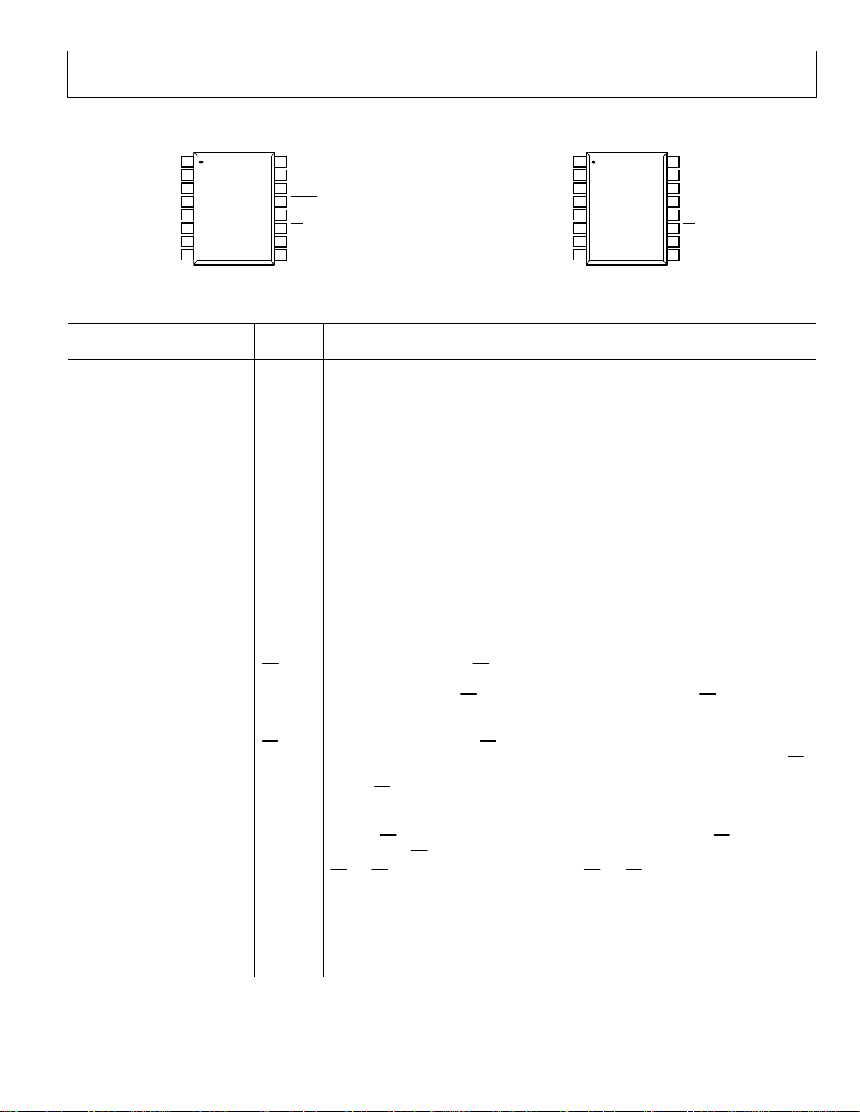
ADM12914
PIN CONFIGURATIONS AND FUNCTION DESCRIPTIONS
VH1
VL1
VH2
VL2
VH3
VL3
VH4
VL4
1
2
3
ADM12914-1
4
TOP VIEW
5
(Not to Scale)
6
7
8
16
15
14
13
12
11
10
9
V
CC
TIMER
SEL
LATCH
UV
OV
REF
GND
08265-002
Figure 2. ADM12914-1 Pin Configuration
Table 4. Pin Function Descriptions
Pin No.
ADM12914-1 ADM12914-2 Mnemonic Description
1, 3 1, 3 VH1, VH2
Voltage High Input 1 and Voltage High Input 2. If the voltage monitored by VH1 or VH2
drops below 0.5 V, an undervoltage condition is detected. Connect to V
2, 4 2, 4 VL1, VL2
Voltage Low Input 1. If the voltage monitored by VL1 or VL2 rises above 0.5 V, an
overvoltage condition is detected. Tie to GND when not in use.
5, 7 5, 7 VH3, VH4
Voltage High Input 3 and Voltage High Input 4. The polarity of these inputs is determined
by the state of the SEL pin (see Table 5). When the monitored input is configured as a
positive voltage and the voltage monitored by VH3 and VH4 drops below 0.5 V, an undervoltage condition is detected. Conversely, when the input is configured as a negative
voltage and the input drops below 0.5 V, an overvoltage condition is detected. Connect
to V
when not in use.
CC
6, 8 6, 8 VL3, VL4
Voltage Low Input 3 and Voltage Low Input 4. The polarity of these inputs is determined
by the state of the SEL pin (see Table 5). When the monitored input is configured as a
positive voltage and the voltage monitored by VL3 or VL4 rises above 0.5 V, an overvoltage
condition is detected. Conversely, when the input is configured as a negative voltage and
the input rises above 0.5 V, an undervoltage condition is detected. Tie to GND when not
in use.
9 9 GND
10 10 REF
Device Ground.
Buffered Reference Output. This pin is a 1 V reference that is used as an offset when
monitoring negative voltages. This pin can source or sink 1 mA, and drive loads up to 1 nF.
Larger capacitive loads may lead to instability. Leave unconnected when not in use.
11 11
Overvoltage Reset Output. OV is asserted low if a negative polarity input voltage drops
OV
below its associated threshold or if a positive polarity input voltage exceeds its threshold.
The ADM12914-1 allows OV
adjustable timeout period determined by the timer capacitor. This pin has a weak pull-up
and can be pulled up to 16 V externally. Leave this pin unconnected when not in use
to V
CC
12 12
Undervoltage Reset Output. UV is asserted low if a negative polarity input voltage exceeds
UV
its associated threshold or if a positive polarity input voltage drops below its threshold. UV
is held low for an adjustable timeout period set by the external capacitor tied to the TIMER
pin. The UV
pin has a weak pull-up to VCC and can be pulled up to 16 V externally via an
external pull-up resistor. Leave this pin unconnected when not in use.
13 N/A1
OV Latch Bypass Input/Clear Pin. When pulled high, the OV latch is cleared. When held
LATCH
high, the OV
output has the same delay and output characteristics as the UV output. When
pulled low, the OV output is latched when asserted. (Applies only to the ADM12914-1.)
N/A1 13 DIS
and UV Disable Input. When pulled high, the OV and UV outputs are held high
OV
irrespective of the state of the VHx and VLx input pins. However, if a UVLO condition occurs,
the OV
and UV outputs are asserted. This pin has a weak internal pull-down (2 µA) to GND.
Leave this pin unconnected when not in use. (Applies only to the ADM12914-2.)
14 14 SEL
Input Polarity Select. This three-state input pin allows the polarity of VH3, VL3, VH4, and VL4
to be configured. Connect this pin to V
possible input polarity configurations (see Tab l e 5).
VH1
VL1
VH2
VL2
VH3
VL3
VH4
VL4
1
2
3
ADM12914-2
4
TOP VIEW
5
(Not to Scale)
6
7
8
16
15
14
13
12
11
10
9
V
CC
TIMER
SEL
DIS
UV
OV
REF
GND
08265-011
Figure 3. ADM12914-2 Pin Configuration
when not in use.
CC
to be latched low. The ADM12914-2 holds OV low for an
or GND, or leave it open to select one of three
CC
Rev. C | Page 5 of 16
Page 6

ADM12914
Pin No.
ADM12914-1 ADM12914-2 Mnemonic Description
15 15 TIMER
16 16 VCC
1
N/A means not applicable.
Adjustable Reset Delay Timer. Connect an external capacitor to the TIMER pin to program
the reset timeout delay. Refer to Figure 15 in the Typical Performance Characteristics
section. Connect this pin to V
Supply Voltage. V
than 6 V, it operates as a shunt regulator. A dropper resistor must be used in this
configuration to limit the current to less than 10 mA. When used without the resistor, the
voltage at this pin must not exceed 6 V. A 0.1 F bypass capacitor or greater should be
used.
to bypass the timer.
CC
operates as a direct supply for voltages up to 6 V. For voltages greater
CC
Rev. C | Page 6 of 16
Page 7

ADM12914
V
TYPICAL PERFORMANCE CHARACTERISTICS
0.505
0.504
0.503
(V)
UOT
0.502
0.501
0.500
0.499
0.498
0.497
THRESHOLD VOLTAGE,
0.496
0.495
–40 –25 –10 1251109580655035205
TEMPERATURE (° C)
Figure 4. Input Threshold Voltage vs. Temperature
8265-012
6.80
6.75
6.70
6.65
(V)
6.60
CC
V
6.55
6.50
6.45
6.40
024681
–40°C
+85°C
+25°C
I
(mA)
CC
Figure 7. VCC Shunt Voltage vs. ICC
0
08265-015
90
85
80
75
70
(µA)
CC
I
65
60
55
50
–40 –25 –10 1251109580655035205
6.80
6.75
6.70
6.65
(V)
6.60
CC
V
6.55
6.50
6.45
6.40
–40 –25 –10 1251109580655035205
VCC = 6V
V
= 3.3V
CC
V
= 2.3V
CC
TEMPERATURE (° C)
Figure 5. Supply Current vs. Temperature
TEMPERATURE ( °C)
Figure 6. VCC Shunt Voltage vs. Temperature
200µA
1mA
2mA
5mA
10mA
1.020
1.015
(V)
1.010
REF
1.005
1.000
0.995
0.990
REFERENCE VOL TAGE, V
0.985
0.980
–40 –25 –10 1251109580655035205
08265-013
TEMPERATURE (° C)
08265-016
Figure 8. Buffered Reference Voltage vs. Temperature
1000
900
800
700
600
500
400
300
TRANSIENT DURATION (µs)
200
100
0
0.1 1 10 100
08265-014
VCC = 6V
VCC = 2.3V
COMPARATOR OV ERDRIVE (% OF V
RESET ASSERTED
ABOVE THE LINE
)
UOT
08265-017
Figure 9. Transient Duration vs. Comparator Overdrive
Rev. C | Page 7 of 16
Page 8

ADM12914
14
13
(ms)
12
UOTO
11
3.0
2.5
(mA)
2.0
UV
1.5
VHx = 0.45V
SEL = V
CC
UV = 150mV
10
9
8
UV/OV TIMEOUT PERIOD, t
7
–40 –25 –10 1251109580655035205
TEMPERATURE (°C)
Figure 10. UV/OV Timeout Period vs. Temperature
0.9
0.8
0.7
0.6
0.5
0.4
0.3
UV VOLTAGE (V)
0.2
0.1
0
–0.1
0 0.1 0.2 0.3 0.4 0.5 0.6 0.7 0.8 0.9 1.0
WITH 10kΩ PULL-UP
WITHOUT PULL-UP
SUPPLY VOLTAGE, V
(V)
CC
Figure 11. UV Output Voltage vs. VCC
1.0
SINK
SINK
, I
– 40°C
(mA)
UV = 50mV
vs. VCC
UV
(V)
CC
+25°C
08265-021
15
8265-022
0.5
PULL-DOW N CURRENT I
0
–0.5
8265-018
012 3456
SUPPLY VOLTAGE, V
Figure 13. I
1000
900
800
700
600
(mV)
OL
500
400
UV/OV, V
300
200
100
0
0510
08265-019
+85°C
I
Figure 14. UV/OV Voltage Output Low vs. Output Sink Current
5.0
VHx = 0.55V
4.5
SEL = V
CC
4.0
3.5
3.0
2.5
2.0
UV VOLTAG E (V)
1.5
1.0
0.5
0
01234
SUPPLY VOLTAGE, V
(V)
CC
Figure 12. UV Output Voltage vs. VCC
5
08265-020
10k
(ms)
1k
UOTO
t
100
10
UV/OV TIMEOUT PERIOD,
1
0.1 1 10 100 1000
TIMER PI N CAPACITANCE C
Figure 15.
UV
/OV Timeout Period vs. Capacitance
TIMER
(nF)
08265-023
Rev. C | Page 8 of 16
Page 9

ADM12914
V
THEORY OF OPERATION
VOLTAGE SUPERVISION
The ADM12914 supervises up to four voltage rails for undervoltage and overvoltage conditions. Two pins, VHx and VLx,
are assigned to monitor each rail, one for overvoltage detection
and the other for undervoltage detection. Each pin is connected
to the input of an internal voltage comparator, and its voltage
level is internally compared with a 0.5 V voltage reference with
very high threshold accuracy of ±0.8%. The device is specified over
the extended operating temperature range from −40°C to +125°C.
The output of each of the internal undervoltage comparators is
tied to a common
internal overvoltage comparators are tied to a common
output pin.
5
3.3V
PSU
2.5V
1.8V
UV
output pin. Likewise, the outputs of the
V
CC
VH1
VL1
VH2
VL2
VH3
VL3
VH4
VL4
ADM12914
SEL
TIMER
UV
OV
LATCH/DIS
OV
SYSTEM
POLARITY CONFIGURATION
The ADM12914 is capable of monitoring supply voltages of
both positive and negative polarities. The SEL pin is a threestate pin that determines the polarity of Input 3 and Input 4. As
summarized in Ta b le 5 , the SEL pin is connected to either GND
or V
, or is not connected.
CC
When an input is configured to monitor a positive voltage, using
the three resistor scheme that is shown in Figure 17, VHx is
connected to the high-side tap of the resistor divider and VLx
is connected to the low-side tap of the resistor divider.
Conversely, when an input is configured to monitor a negative
voltage, UVx and OVx are swapped internally. The negative
voltage for monitoring is then connected as shown in Figure 18.
VHx remains connected to the high-side tap and VLx remains
connected to the low-side tap. Within this configuration, an
undervoltage condition occurs when the monitored voltage is less
negative than the programmed threshold, and an overvoltage
condition occurs when the monitored voltage is more negative
than the programmed threshold.
REF
Figure 16. Typical Applications Diagram
GND
08265-003
Table 5. Polarity Configuration
Input 3 Input 4
SEL Pin Polarity UV Condition OV Condition Polarity UV Condition OV Condition
Connected to VCC Positive VH3 < 0.5 V VL3 > 0.5 V Positive VH4 < 0.5 V VL4 > 0.5 V
Left Unconnected Positive VH3 < 0.5 V VL3 > 0.5 V Negative VL4 > 0.5 V VH4 < 0.5 V
Connected to GND Negative VL3 > 0.5 V VH3 < 0.5 V Negative VL4 > 0.5 V VH4 < 0.5 V
Rev. C | Page 9 of 16
Page 10

ADM12914
V
V
M
(
M
MONITORING PIN CONNECTIONS
Positive Voltage Monitoring Scheme
When monitoring a positive supply, the desired nominal
operating voltage for monitoring is denoted by V
nominal current through the resistor divider, V
voltage trip point, and V
R
X
PH
R
Y
V
PL
R
Z
Figure 17. Positive Undervoltage/Overvoltage Monitoring Configuration
is the undervoltage trip point.
UV
M
ADM12914
VHx
VLx
UVx
0.5V
OVx
Figure 17 illustrates the positive voltage monitoring input connection. Three external resistors, R
positive voltage for monitoring,V
V
, and low-side voltage, VPL. The high-side voltage is con-
PH
, RY, and RZ, divide the
X
, into high-side voltage,
M
nected to the corresponding VHx pin and the low-side voltage
is connected to the corresponding VLx pin.
To trigger an overvoltage condition, the low-side voltage (in this
case, V
low-side voltage, V
) must exceed the 0.5 V threshold on the VLx pin. The
PL
, is given by the following equation:
PL
⎛
R
⎜
=
VV
PL
OV
⎜
⎝
⎞
Z
⎟
V5.0=
⎟
++
RRR
YX
Z
⎠
Also,
V
M
I
Therefore, R
RRR =++
YX
Z
, which sets the desired trip point for the overvoltage
Z
monitor, is calculated using the following equation:
VR)5.0(
()
M
=
Z
()
OV
(1)
()
IV
M
To trigger the undervoltage condition, the high-side voltage,
V
, must exceed the 0.5 V threshold on the VHx pin. The
PH
high-side voltage, V
VV
=
UVPH
Because R
is already known, RY can be expressed as follows:
Z
R −=
Y
()
, is given by the following equation:
PH
⎛
+
Y
⎜
⎜
⎝
V
)5.0(
()
M
R
IV
()
MUV
⎞
RR
Z
⎟
V5.0=
⎟
RRR
++
YX
Z
⎠
(2)
Z
, IM is the
M
is the over-
OV
8265-004
When R
and RZ are known, RX is calculated using the following
Y
formula:
V
)
X
M
I
()
R −−= (3)
, IM, VOV, or VUV change, each step must be recalculated.
If V
M
RR
Y
Z
Negative Voltage Monitoring Scheme
Figure 18 shows the circuit configuration for negative supply
voltage monitoring. To monitor a negative voltage, a 1 V reference
voltage is required to connect to the end node of the voltage
divider circuit. This reference voltage is generated internally
and is output through the REF pin.
ADM12914
REF
R
Z
V
NH
R
V
R
Figure 18. Negative Undervoltage/Overvoltage Monitoring Configuration
VHx
Y
NL
VLx
X
V
M
0.5V
OVx
UVx
8265-005
The equations described previously in the Positive Voltage
Monitoring Scheme section need some minor modifications for
use with negative voltage monitoring. The 1 V reference voltage
is added to the overall voltage drop; it must therefore be subtracted from V
, VUV, and VOV before using each in the previous
M
equations.
To monitor a negative voltage level, the resistor divider circuit
divides the voltage differential level between the 1 V reference
voltage and the negative supply voltage into high-side voltage,
, and low-side voltage, VNL. Similar to the positive voltage
V
NH
monitoring scheme, the high-side voltage, V
the corresponding VHx pin and the low-side voltage, V
, is connected to
NH
NL
, is
connected to the corresponding VLx pin. Refer to the Vo lt a ge
Monitoring Example section for further information.
THRESHOLD ACCURACY
The reset threshold accuracy is fundamental, especially at lower
voltage levels. Consider an FPGA application that requires a 1 V
core voltage input with a tolerance of ±5%, where the supply has
a specified regulation, for example, ±2.6%. As shown in Figure 19,
to ensure the supply is within the FPGA input voltage requirement
range, its voltage level must be monitored for UV and OV conditions. The voltage swing on the supply itself causes the voltage
band available for setting the monitoring threshold to be quite
narrow. In this example, the threshold voltages, including the
Rev. C | Page 10 of 16
Page 11

ADM12914
tolerances, must fit within a monitor region of just 0.024 V. The
ADM12914 device with 0.1% resistors can achieve this level of
accuracy.
VOLTAGE
1.05V
1.026V
1V CORE
VOLTAGE
0.974V
0.95V
UV
+5%
–5%
2.4% RANGE FOR OV MONITORING
+2.6% SUPPLY REGULATION
TOLERANCE
–2.6% SUPPLY REGULATION
2.4% RANGE FOR UV MONITO RING
TOLERANCE
Figure 19. Monitoring Accuracy Example
t
UOTO
TIME
08265-006
VOLTAGE MONITORING EXAMPLE
To illustrate how the ADM12914 device works in a real-world
application, consider the 1 V input example shown in Figure 19,
with the addition of a −5 V rail.
The first step is to choose the current flow through both voltage
divider circuits, for example, 5 µA.
For the 1 V ± 5% input, due to the specified ±2.6% regulation of
the supply, the UV and OV threshold should be set in the middle
of the undervoltage and overvoltage monitoring bands, respectively; in this case, on the ±3.8% points of the supply, which are
0.962 V for the UV threshold and 1.038 V for OV threshold.
Input these values into Equation 1 to Equation 3 as follows:
=
R (1)
Z
Insert the value of R
=
R
Y
)1)(5.0(
6
−
)105)(038.1(
×
into Equation 2.
Z
)1)(5.0(
6
−
)105)(962.0(
×
Then substitute the calculated values for R
Equation 3.
1
=
R
X
6
−
105
×
This design approach meets the application specifications. As
described previously, the 1 V rail is specified with an input
requirement of ±5% and a supply tolerance of ±2.6%. This
effectively means the OV threshold of the monitoring device,
including all the tolerance factors, must fit within the 1.026 V
to 1.05 V range. Similarly, the UV threshold range must be
between 0.95 V and 0.974 V.
k5.96
≈
≈−
k7.41k5.96
and RY into
Z
k5.96k7.41k5.96
≈−−
(2)
(3)
The four worst-case scenarios of minimum and maximum
undervoltage and overvoltage thresholds are calculated as follows:
Minimum overvoltage threshold
⎛
_
MINOV
VV
⎛
1496.0
+=
⎜
⎜
⎝
⎜
+−=
1%)8.05.0(
⎜
⎝
+
)999.0)(7410500,96(
⎞
⎟
⎟
)001.1)(500,96(
⎠
RR
−+−
YX
R
+
%)1.0(
Z
⎞
%)1.0(%)1.0(
⎟
⎟
⎠
=1.029 V > 1.026 V
Maximum overvoltage threshold
⎛
⎜
1%)8.05.0(
_
MAXOV
VV
++=
⎜
⎝
R
Z
+++
RR
YX
%)1.0(
−
⎞
%)1.0(%)1.0(
⎟
⎟
⎠
= 1.047 V < 1.05 V
The maximum and minimum overvoltage threshold values
reside within the 1.026 V to 1.05 V range specified.
The minimum and maximum undervoltage thresholds are
calculated as follows:
Minimum undervoltage threshold
⎛
⎜
V
_
MINUV
1%)8.0V5.0(
+−=
⎜
⎝
R
Y
%)1.0(
−
X
RR
+++
Z
⎞
⎟
⎟
%)1.0(%)1.0(
⎠
= 0.9557 V > 0.95 V
Maximum undervoltage threshold
+
⎛
⎜
++=
V
_
MAXUV
1%)8.0V5.0(
⎜
⎝
R
Y
%)1.0(
X
RR
Z
⎞
⎟
⎟
−+−
%)1.0(%)1.0(
⎠
= 0.9729 V < 0.974 V
These values fit within the specified undervoltage monitoring
range. All four worst-case scenarios satisfy the tolerance
requirement; therefore, the design approach is valid.
–5V RAIL
1V RAIL
5V
96.5kΩ
7.41kΩ
96.5kΩ
Figure 20. Positive and Negative Supply Monitor Example
1.09MΩ
14.3kΩ
93.1kΩ
VH1
VL1
ADM12914
VL3
VH3
REF
V
CC
GND
OV
SEL
UV
08265-007
Rev. C | Page 11 of 16
Page 12

ADM12914
(
)
(
)
V
V
Next, consider a −5 V input, which is specified with a ±12%
input. The threshold accuracy required by the supply is chosen
to be within ±5% of the −5 V rail. The UV and OV threshold
should be set in the middle of the undervoltage and overvoltage
monitoring bands, respectively. In this case, on the ±8.5%
points of the supply, which is −4.575 V for the UV threshold
and −5.425 V for the OV threshold.
The negative voltage scheme configuration requires that the 1 V
reference voltage be accounted for in Equation 1 to Equation 3.
The 1 V reference voltage is subtracted from V
and the absolute value of the result is taken.
Equation 1 becomes
−−
=
R
Z
()
Insert the value of R
=
R
Y
()
To c al c ul ate R
R
X
, insert the value of RZ and RY into Equation 3.
X
()
15
−−
=
6
−
105
×
15)5.0(
()
×−−
1051425.5
into Equation 2
Z
15)5.0(
−−
()
1051575.4
×−−
≈
−
6
6
−
()()
POWER-UP AND POWER-DOWN
On power-up, when VCC reaches 1 V, the active low UV output
OV
asserts and the
the V
pin reaches 1 V, the ADM12914 is guaranteed to assert
CC
UV
low and OV high. When VCC exceeds 1.9 V (minimum), the
output pulls up to VCC. When the voltage on
VHx and VLx inputs take control. When V
VHx inputs are valid, an internal timer begins. Subsequent to
UV
an adjustable time delay,
weakly pulls high.
UV/OV TIMING CHARACTERISTICS
UV
is an active low output. It asserts when any of the four monitored voltages is below its associated threshold. When the
voltage on the V
UV
holds
low for an adjustable period, t
on all the monitoring rails rise above their thresholds. This
allows time for all monitored power supplies to stabilize after
power-up. Similarly, any monitored voltage that falls below its
threshold initiates a timer reset, and the internal timer restarts
once all the monitoring rails rise above their thresholds.
UV
The
and OV outputs are held asserted after all faults have
cleared for an adjustable timeout period, determined by the
value of the external capacitor attached to the TIMER pin.
pin is greater than 2 V, an internal timer
CC
, VUV, and VOV,
M
kΩ1.93
kΩ3.14kΩ1.93
≈−
MΩ09.1Ωk1.93Ωk3.14
≈−−
and each of the
CC
, after the voltages
UOTO
TIMER CAPACITOR SELECTION
The UV and OV timeout period on the ADM12914 is programmable via the external timer capacitor, C
the TIMER pin and ground. The timeout period, t
calculated using the following equation:
C
TIMER
= (t
)(115)(10−9) F/sec
UOTO
Refer to Figure 15 in the Typical Performance Characteristics
section, which illustrates the delay time as a function of the
timer capacitor value. A minimum capacitor value of 10 pF is
required. The chosen timer capacitor must have a leakage current
that is less than the 1.7 μA TIMER pin charging current. To
bypass the timeout period, connect the TIMER pin to V
Hx MONITO R TI M I NG
V
VHx
UOT
t
UOD
t
V
t
V
UOD
V
UOT
UOD
UOT
UOT
t
1V
1V
1V
UOD
1V
VHx MONITOR TIMING
(TIMER PIN TIED TO V
Lx MONITOR TIMING
VLx MONITOR TIMI NG
(TIMER PIN TIED TO V
UV
VHx
UV
NOTES
1. WHEN AN I NP UT IS CONFIGURED TO MONITOR A NE GATIVE
VOLTAG E , VHx TRIG GERS AN OVERVOLTAGE CONDITIO N.
Figure 21. VHx Positive Voltage Monitoring Timing Diagrams
VLx
OV
VLx
OV
NOTES
1. WHEN AN I NP UT IS CONFIGURED TO M ONITOR A NEGATIVE
VOLTAG E , VLx TRIGGERS AN UNDERVO LTAGE CONDITION.
Figure 22. VLx Positive Voltage Monitoring Timing Diagrams
t
t
UOTO
UOTO
TIMER
)
CC
t
UOD
)
CC
t
UOD
, placed between
, is
UOTO
.
CC
08265-026
08265-027
Rev. C | Page 12 of 16
Page 13

ADM12914
V
V
−
=
UV AND OV RISE AND FALL TIMES
The UV or OV output rise times (from 10% to 90%) can be
approximated using the following equation:
t
≈ 2.2(R
R
PULL-UP
)(C
LOAD
)
where:
R
is the internal weak pull-up resistance with an approx-
PULL-UP
imate value of 400 kΩ at room temperature with V
C
is the external load capacitance on the output pin.
LOAD
UV
When a fault occurs, the
or OV output fall time can be
> 1 V.
CC
expressed as
t
where
≈ 2.2(R
F
R
PULL-DOWN
PULL-DOWN
)(C
)
LOAD
is the internal pull-down resistance, which is
approximately 50 Ω. Assuming a load capacitance of 150 pF, the
fall time is 16.5 ns.
UV/OV OUTPUT CHARACTERISTICS
Both the OV and UV outputs have strong pull-down to ground
and weak internal pull-up to V
. This permits the pins to behave
CC
as open-drain outputs. When the rise time on the pin is not
critical, the weak pull-up removes the requirement for an
external pull-up resistor. The open-drain configuration allows
for wire-OR’ing of outputs, which is particularly useful when
more than one signal needs to pull down on the output.
At V
= 1 V, a maximum VOL = 0.15 V at UV is guaranteed. At
CC
= 1 V, the weak pull-up current on OV is almost turned on.
V
CC
OV
Consequently, if the state and pull-up strength of the
important at very low V
, an external pull-up resistor of no more
CC
pin is
than 100 kΩ is advised. By adding an external pull-up resistor,
the pull-up strength on the
OV
pin is greater. Therefore, if it is
connected in a wire-OR’ed configuration, the pull-down strength
of any single device must account for this additional pull-up
strength.
GLITCH IMMUNITY
The ADM12914 is immune to short transients that may occur
on the monitored voltage rails. The device contains internal
filtering circuitry that provides immunity to fast transient
glitches. Figure 9 illustrates glitch immunity performance by
showing the maximum transient duration without causing a
reset pulse. Glitch immunity makes the ADM12914 suitable for
use in noisy environments.
UNDERVOLTAGE LOCKOUT (UVLO)
The ADM12914 has an undervoltage lockout circuit that monitors
the voltage on the V
1.94 V (minimum), the circuit activates. The
OV
and the
recovers, UV exhibits the same timing characteristics as
V
CC
output is cleared and is not allowed to assert. When
though an undervoltage condition had occurred on the inputs.
pin. When the voltage on VCC drops below
CC
UV
output is asserted
SHUNT REGULATOR
The ADM12914 is powered via the VCC pin. The VCC pin can
be directly connected to a voltage rail of up to 6 V. In this
mode, the supply current of the device does not exceed 100
µA. An internal shunt regulator allows the ADM12914 to
operate at voltage levels greater than 6V by simply placing a
dropper resistor in series between the supply rail and the V
CC
pin to limit the input current to less than 10 mA.
Once the supply voltage, V
, has been established, an
IN
appropriate value for the dropper resistor can be calculated.
Begin by determining the maximum supply current
required, I
, by adding the current drawn from the
CCtotal
reference and/or the pull resistors between the outputs and
pin to the maximum specified supply current. The
the V
CC
minimum and maximum shunt regulator voltage specified
in Table 1, V
SHUNT min
and V
SHUNT max
, are also required in the
following calculations.
Calculate the maximum and minimum dropper resistor
values
R−=
MAX
=
R
MIN
INmin
INmax
I
CCtotal
VV
SHUNTmax
SHUNTmin
100
Based on these values, choose a real-world resistor value
within this range. Then, given the specified accuracy of this
resistor, calculate the minimum and maximum real resistor
value variation, R
REALmin
and R
, respectively.
REALmax
The maximum device power is calculated as follows:
DeviceMax
=
VP
SHUNTmax
SHUNTmax
IV
CCtotal
⎡
()
−
VV
IN
max
R
REAL
SHUNTmax
min
⎢
⎣
−
Icc
TOTAL
⎤
+
⎥
⎦
To check that the calculated value of the resistor will be
acceptable, calculate the maximum device temperature rise
PθTemp
JARISEmax
DeviceMax
Add this value to the ambient operating temperature. If the
resistor value is acceptable, the result will lie within the
specified operating temperature range of the device.
OV LATCH (ADM12914-1)
If an overvoltage condition occurs when the
OV
pulled low, the
the latch. If an
latch is bypassed and the
UV
pin, with an identical timeout period. If the
pin latches low. Pulling
OV
condition clears while
OV
pin behaves in the same way as the
pulled low while the timeout period is active, the
low, as in normal operation.
LATCH
LATCH
LATCH
OV
pin is
high clears
is high, the
LATCH
pin is
pin latches
Rev. C | Page 13 of 16
Page 14

ADM12914
DISABLE (ADM12914-2)
Pulling the DIS pin high disables both the UV and OV outputs,
and forces both outputs to remain weakly pulled high, regardless of any faults that are detected at the inputs. If a UVLO
condition is detected, the
UV
output is asserted and pulls low;
however, the timeout function is bypassed. As soon as the
UVLO condition clears, the
normal operation when the pin is left unconnected, DIS has a
weak 2 µA internal pull-down current.
UV
output pulls high. To guarantee
Rev. C | Page 14 of 16
Page 15

ADM12914
V
TYPICAL APPLICATIONS
5
3.3V
PSU
2.5V
1.8V
312kΩ
V
CC
ADM12914
LATCH/DIS
SEL
TIMER
SYSTEM
UV
OV
2.37kΩ
33.6kΩ
200kΩ
2.34kΩ
34.8kΩ
111kΩ
1.82kΩ
27.1kΩ
120kΩ
3.05kΩ
VH1
VL1
VH2
VL2
VH3
VL3
VH4
VL4
45.3kΩ
REF
GND
08265-008
Figure 23. Typical Application Diagram for Monitoring 5 V, 3.3 V, 2.5 V, and 1.8 V with 1.5% Supply Tolerance and 5% Input Tolerance Requirement
+12V
PSU
–12V
1.98MΩ
5.62kΩ
83.5kΩ
51.7kΩ
12kΩ
1420kΩ
VH1
VL1
VH2
ADM12914
VL2
VH3
VL3
VH4
VL4
REF
1kΩ
V
CC
LATCH/DIS
GND
SEL
TIMER
UV
OV
SYSTEM
8265-009
Figure 24. Typical Application Diagram for Monitoring 12 V with 1.5% Supply Tolerance and 5% Input Tolerance Requirement;
−12 V with 3% Supply Tolerance and 15% Input Tolerance Requirement
Rev. C | Page 15 of 16
Page 16

ADM12914
OUTLINE DIMENSIONS
0.065 (1.65)
0.049 (1.25)
0.010 (0.25)
0.004 (0.10)
COPLANARIT Y
0.004 (0.10)
0.197 (5.00)
0.193 (4.90)
0.189 (4.80)
16
1
0.025 (0.64)
BSC
CONTROLL ING DIMENSIONS ARE IN INCHES; MIL LIMETERS DIMENSIO NS
(IN PARENTHESES) ARE ROUNDED-O FF INCH EQ UIVALENTS FOR
REFERENCE ON LY AND ARE NOT APPROPRI ATE FOR USE IN DESIGN.
9
0.158 (4.01)
0.154 (3.91)
0.150 (3.81)
8
SEATING
0.012 (0.30)
0.008 (0.20)
COMPLIANT TO JEDEC STANDARDS MO-137-AB
PLANE
0.069 (1.75)
0.053 (1.35)
0.244 (6.20)
0.236 (5.99)
0.228 (5.79)
8°
0°
0.010 (0.25)
0.006 (0.15)
0.050 (1.27)
0.016 (0.41)
Figure 25. 16-Lead Shrink Small Outline Package [QSOP]
(RQ-16)
Dimensions shown in inches and (millimeters)
0.020 (0.51)
0.010 (0.25)
0.041 (1.04)
REF
012808-A
ORDERING GUIDE
Model1 Temperature Range Package Description Package Option
ADM12914-1ARQZ −40°C to +125°C 16-Lead Shrink Small Outline Package [QSOP] RQ-16
ADM12914-1ARQZ-RL7 −40°C to +125°C 16-Lead Shrink Small Outline Package [QSOP] RQ-16
ADM12914-2ARQZ −40°C to +125°C 16-Lead Shrink Small Outline Package [QSOP] RQ-16
ADM12914-2ARQZ-RL7 −40°C to +125°C 16-Lead Shrink Small Outline Package [QSOP] RQ-16
1
Z = RoHS Compliant Part.
©2009-2010 Analog Devices, Inc. All rights reserved. Trademarks and
registered trademarks are the property of their respective owners.
D08265-0-6/10(C)
Rev. C | Page 16 of 16
 Loading...