

Page 1
Hot-Swap Controller and Digital Power
ADM1275
Q
1
GATE
SENSE+
TIMER
TIMER
ADM1275-1
GND
R
SENSE
SENSE–
VCC
V
CP
2V TO 20V
2.95V
TO
20V
VCAP
IOUT
UV
OV
1.0V
1.0V
VOUT
VOUT
12-BIT
ADC
SCL
SDA
ADR
SENSE+
IOUT
LDO
CHARGE
PUMP
TIMEOUT
GPO2/ALERT2
PWRGD
GPO1/ALERT1/CONV
LATCH
TIMER
ON
TIMER
ON
V
CBOS
SS
CURRENT
LIMIT
FLB
ISET
TIMEOUT
CURRENT
LIMIT
CONTROL
REF
SELECT
1.0V
GATE
DRIVE/
LOGIC
LOGIC
AND
PMBus
×50
+
+
–
–
+
–
+
–
08931-001
FEATURES
Controls supply voltages from 2 V to 20 V
370 ns response time to short circuit
Resistor-programmable 5 mV to 25 mV current limit
±1% accurate, 12-bit ADC for current, V
Charge-pumped gate drive for multiple external N-channel FETs
High gate drive voltage to ensure lowest R
Foldback for tighter FET SOA protection
Automatic retry or latch-off on current fault
Programmable current limit timer for SOA
Programmable, multifunction GPOs
Power-good status output
Analog UV and OV protection
ENABLE pin (ADM1275-3 only)
Peak detect registers for current and voltage
PMBus fast mode compliant interface
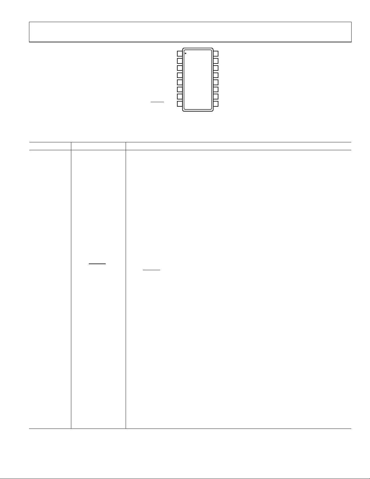
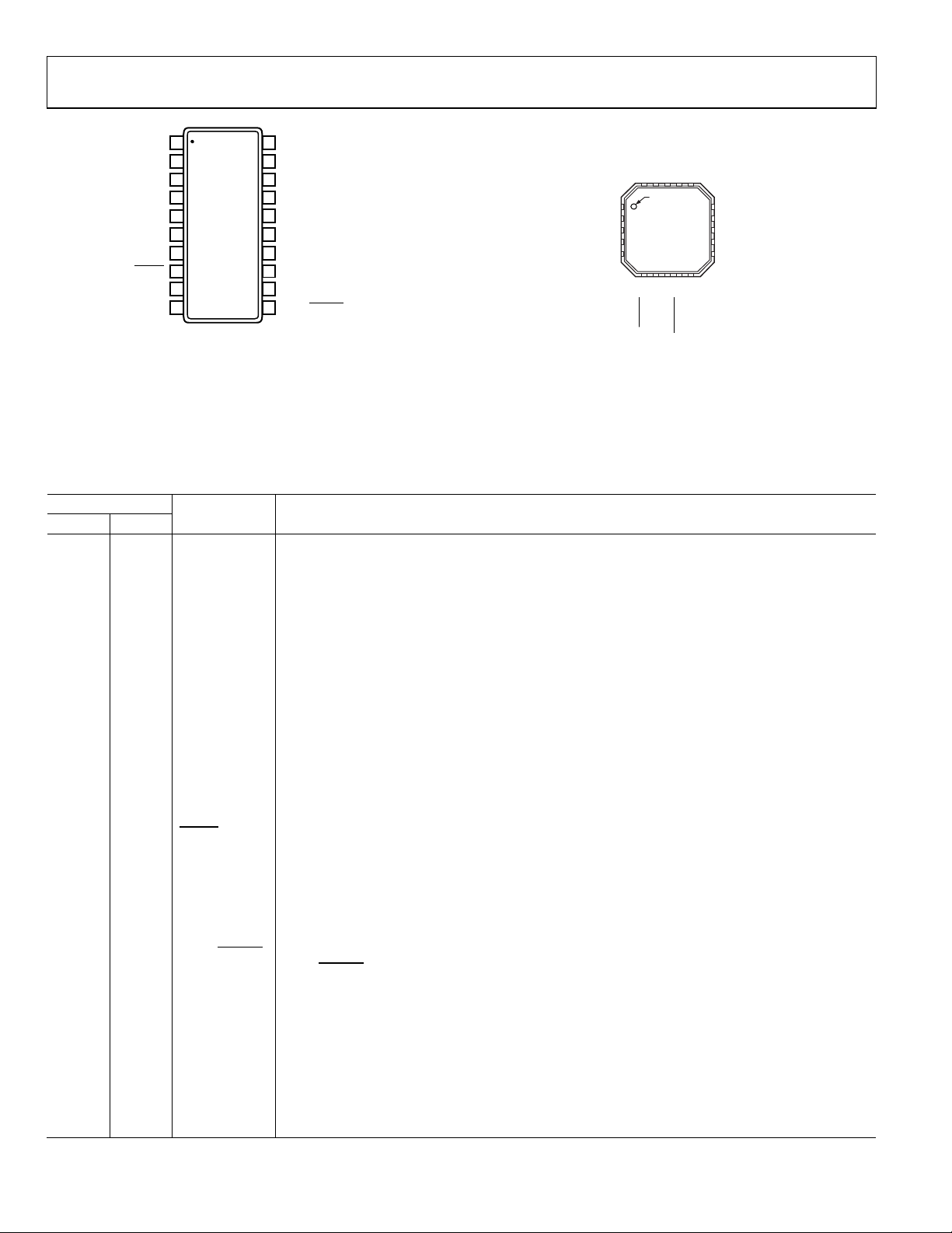
16-lead QSOP and 20-lead QSOP and LFCSP
APPLICATIONS
Power monitoring and control/power budgeting
Central office equipment
Telecommunication and data communication equipment
PCs/servers
IN/VOUT
DSON
readback
Monitor with PMBus Interface
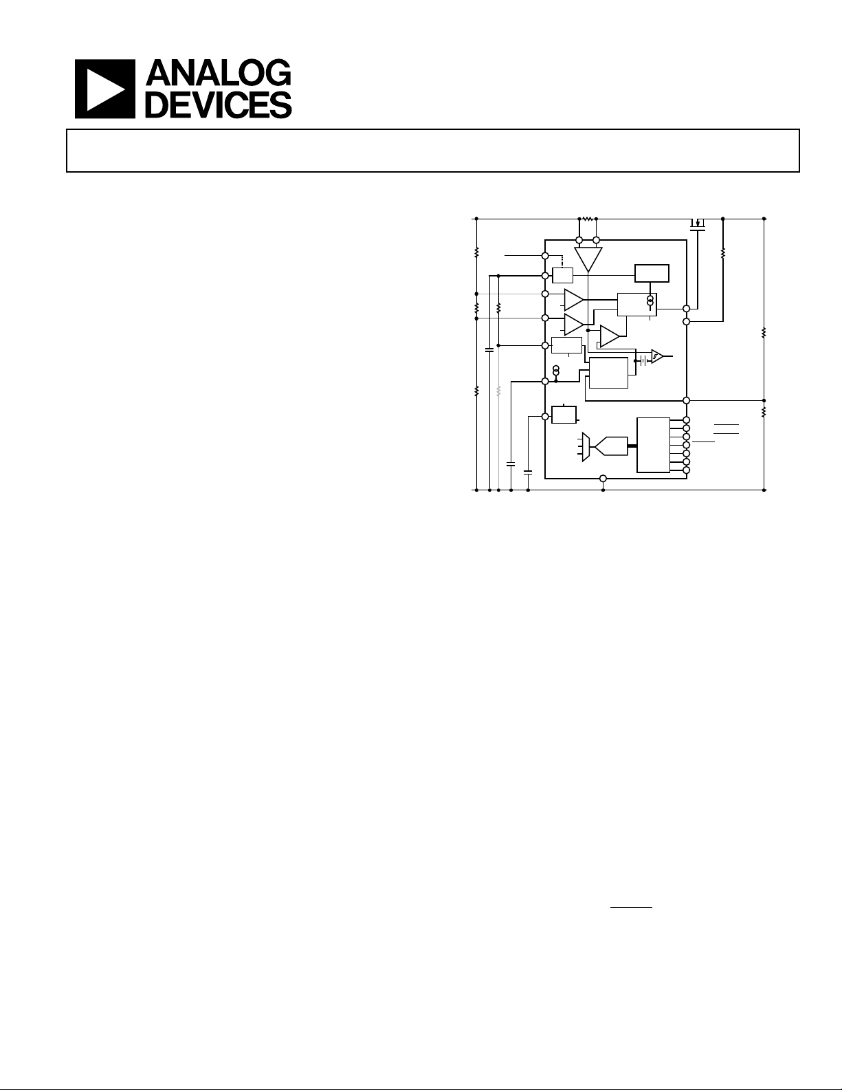
APPLICATIONS DIAGRAM
Figure 1.
GENERAL DESCRIPTION
The ADM1275 is a hot-swap controller that allows a circuit board
to be removed from or inserted into a live backplane. It also features
current and voltage readback via an integrated 12-bit analog-todigital converter (ADC), accessed using a PMBus™ interface.
The load current is measured using an internal current sense
amplifier that measures the voltage across a sense resistor in
the power path via the SENSE+ and SENSE− pins. A default
limit of 20 mV is set, but this limit can be adjusted, if required,
using a resistor divider network from the internal reference
voltage to the ISET pin.
The ADM1275 limits the current through the sense resistor by
controlling the gate voltage of an external N-channel FET in the
power path, via the GATE pin. The sense voltage—and, therefore,
the load current—is maintained below the preset maximum. The
ADM1275 protects the external FET by limiting the time that the
FET remains on while the current is at its maximum value. This
current limit time is set by the choice of capacitor connected to
the TIMER pin. In addition, a foldback resistor network can be
used to actively lower the current limit as the voltage across the
FET is increased. This helps to maintain constant power in the
FET and allows the safe operating area (SOA) to be adhered to
in an effective manner.
Rev. B
Information furnished by Analog Devices is believed to be accurate and reliable. However, no
responsibility is assumed by Analog Devices for its use, nor for any infringements of patents or other
rights of third parties that may result from its use. Specifications subject to change without notice. No
license is granted by implication or otherwise under any patent or patent rights of Analog Devices.
Trademarks and registered trademarks are the property of their respective owners.
In case of a short-circuit event, a fast internal overcurrent detector responds within 370 ns and signals the gate to shut down. A
1500 mA pull-down device ensures a fast FET response. The
ADM1275 features overvoltage and undervoltage protection,
programmed using external resistor dividers on the UV and OV
pins. A PWRGD signal can be used to detect when the output
supply is valid, using the FLB pin to monitor the output. GPO
pins can be configured as various output signals that can be
asserted when a programmed current or voltage level is reached.
The 12-bit ADC can measure the current in the sense resistor,
as well as the supply voltage on the SENSE+ pin or the output
voltage. A PMBus interface allows a controller to read current
and voltage data from the ADC. Measurements can be initiated
by a PMBus command. Alternatively, the ADC can run continuously, and the user can read the latest conversion data whenever
required. Up to four unique PMBus addresses can be selected,
depending on the way that the ADR pin is connected.
The ADM1275-1 and ADM1275-3 are available in a 20-lead QSOP
and 20-lead LFCSP and have a
for automatic retry or latch-off when an overcurrent fault occurs.
The ADM1275-2 is available in a 16-lead QSOP with latch-off
mode only.
One Technology Way, P.O. Box 9106, Norwood, MA 02062-9106, U.S.A.
Tel: 781.329.4700
Fax: 781.461.3113 ©2010–2011 Analog Devices, Inc. All rights reserved.
LATCH
pin that can be configured
www.analog.com
Page 2

ADM1275
TABLE OF CONTENTS
Features .............................................................................................. 1
Applications ....................................................................................... 1
Applications Diagram ...................................................................... 1
General Description ......................................................................... 1
Revision History ............................................................................... 3
Specifications ..................................................................................... 4
Serial Bus Timing Characteristics .............................................. 7
Absolute Maximum Ratings ............................................................ 8
Thermal Characteristics .............................................................. 8
ESD Caution .................................................................................. 8
Pin Configurations and Function Descriptions ........................... 9
Typical Performance Characteristics ........................................... 14
Functional Block Diagrams ........................................................... 20
Theory of Operation ...................................................................... 21
Powering the ADM1275 ............................................................ 21
Current Sense Inputs .................................................................. 21
Current Limit Reference ............................................................ 22
Setting the Current Limit (ISET).............................................. 22
Soft Start ...................................................................................... 23
Foldback ....................................................................................... 23
Timer ............................................................................................ 24
Hot-Swap Retry Duty Cycle ...................................................... 24
FET Gate Drive Clamps ............................................................. 24
Fast Response to Severe Overcurrent ...................................... 25
Undervoltage and Overvoltage ................................................. 25
ENABLE Input (ADM1275-3 Only) ........................................ 25
Power Good ................................................................................. 25
VOUT Measurement ................................................................. 26
FET Health .................................................................................. 26
Power Monitor ............................................................................ 26
PMBus Interface ............................................................................. 27
Device Addressing ...................................................................... 27
SMBus Protocol Usage ............................................................... 27
Packet Error Checking ............................................................... 27
SMBus Message Formats ........................................................... 28
Group Commands ...................................................................... 29
Hot-Swap Control Commands ................................................. 30
ADM1275 Information Commands ........................................ 30
Status Commands ....................................................................... 30
GPO and Alert Pin Setup Commands ..................................... 31
Rev. B | Page 2 of 48
Power Monitor Commands ...................................................... 31
Warning Limit Setup Commands ............................................ 32
PMBus Direct Format Conversion .......................................... 32
Voltage and Current Conversion using LSB values ............... 33
ADM1275 Alert Pin Behavior ...................................................... 34
Faults and Warnings .................................................................. 34
Generating an Alert ................................................................... 34
Handling/Clearing an Alert ...................................................... 34
SMBus Alert Response Address ............................................... 35
Example Use of SMBus Alert Response Address ................... 35
PMBus Command Reference........................................................ 36
OPERATION .............................................................................. 37
CLEAR_FAULTS ........................................................................ 37
CAPABILITY .............................................................................. 37
VOUT_OV_WARN_LIMIT ..................................................... 37
VOUT_UV_WARN_LIMIT ..................................................... 37
IOUT_OC_WARN_LIMIT ...................................................... 37
IOUT_WARN2_LIMIT ............................................................. 38
VIN_OV_WARN_LIMIT ......................................................... 38
VIN_UV_WARN_LIMIT ......................................................... 38
STATUS_BYTE .......................................................................... 38
STAT US_WORD ........................................................................ 38
STATUS_VOUT ......................................................................... 39
STATUS_IOUT .......................................................................... 39
STATUS_INPUT ........................................................................ 39
STATUS_MFR_SPECIFIC ........................................................ 40
READ_VIN ................................................................................. 40
READ_VOUT ............................................................................. 41
READ_IOUT .............................................................................. 41
PMBUS_REVISION .................................................................. 41
MFR_ID ....................................................................................... 41
MFR_MODEL ............................................................................ 41
MFR_REVISION ........................................................................ 42
PEAK_IOUT ............................................................................... 42
PEAK_VIN.................................................................................. 42
PEAK_VOUT ............................................................................. 42
PMON_CONTROL ................................................................... 42
PMON_CONFIG ....................................................................... 43
ALERT1_CONFIG ..................................................................... 43
ALERT2_CONFIG ..................................................................... 44
Page 3

ADM1275
DEVICE_CONFIG ..................................................................... 45
POWER_CYCLE ......................................................................... 45
REVISION HISTORY
6/11—Rev. A to Rev. B
Changes to t
Added Conditions Statement to Table 2 ....................................... 7
Changes to VOUT Pin Description, Table 5 ............................... 10
Changes to VOUT Pin Description, Table 6 ............................... 13
Changes to Figure 42 ..................................................................... 19
Changes to Current Sense Inputs Section .................................... 21
Added PMBus Direct Format Conversion Section..................... 32
Added Voltage and Current Conversion Using LSB
Values Section .................................................................................. 33
Changes to Handling/Clearing and Alert Section ...................... 34
10/10—Rev. 0 to Rev. A
Added 20-Lead LFCSP ...................................................... Universal
Changes to Table 4 ............................................................................ 8
Added Figure 4; Renumbered Figures Sequentially ..................... 9
Changes to Table 5 ............................................................................ 9
Added Table 6; Renumbered Tables Sequentially ....................... 11
Added Figure 7 and Table 7 ........................................................... 12
Updated Outline Dimensions ........................................................ 48
Changes to Ordering Guide ........................................................... 48
9/10—Revision 0: Initial Version
Parameter ................................................................ 7
BUF
Outline Dimensions ........................................................................ 46
Ordering Guide ........................................................................... 47
Rev. B | Page 3 of 48
Page 4

ADM1275
SPECIFICATIONS
VCC = 2.95 V to 20 V, VCC ≥ V
Table 1.
Parameter Min Typ Max Unit Test Conditions/Comments
POWER SUPPLY
Operating Voltage Range, VCC 2.95 20 V
Undervoltage Lockout 2.4 2.7 V VCC rising
Undervoltage Hysteresis 90 120 mV
Quiescent Current, ICC 5 mA GATE on and power monitor running
UV PIN
Input Current, IUV 100 nA UV ≤ 3.6 V
UV Threshold, UVTH 0.97 1.0 1.03 V UV falling
UV Threshold Hysteresis, UV
UV Glitch Filter, UVGF 2 7 μs 50 mV overdrive
UV Propagation Delay, UVPD 5 8 μs UV low to GATE pull-down active
OV PIN ADM1275-1 and ADM1275-3
Input Current, IOV 100 nA OV ≤ 3.6 V
OV Threshold, O VTH 0.97 1.0 1.03 V OV rising
OV Threshold Hysteresis, OV
OV Glitch Filter, OVGF 0.5 1.5 μs 50 mV overdrive
OV Propagation Delay, OVPD 1.0 2 μs OV high to GATE pull-down active
SENSE+ AND SENSE− PINS
Input Current, I
Input Imbalance, I
150 μA Per individual pin; SENSE+, SENSE− = 20 V
SENSEx
5 μA I
ΔSENSE
VCAP PIN
Internally Regulated Voltage, V
ISET PIN
Reference Select Threshold, V
Internal Reference, V
1 V Accuracies included in total sense voltage accuracies
CLREF
Gain of Current Sense Amplifier, AV
Input Current, I
100 nA V
ISET
GAT E PIN Maximum voltage on the gate is always clamped to ≤31 V
Gate Drive Voltage, ΔV
GAT E
10 12 14 V 17 V ≥ VCC ≥ 8 V; I
4.5 13 V 20 V ≥ VCC ≥ 17 V; I
8 10 V V
4.5 6 V V
Gate Pull-Up Current, I
GAT EU P
Gate Pull-Down Current, I
Gate Pull-Down Current, I
Gate Pull-Down Current, I
Gate Holdoff Resistance 20 Ω VCC = 0 V
HOT-SWAP SENSE VOLTAGE
Hot-Swap Sense Voltage Current Limit,
V
SENSECL
Foldback Inactive V
24.6 25 25.4 mV V
19.6 20 20.4 mV V
9.6 10 10.4 mV V
4.6 5 5.4 mV V
Foldback Active 3.5 4 4.5 mV V
9.6 10 10.4 mV V
, V
SENSE+
40 50 60 mV
HYST
50 60 70 mV
HYST
VCAP
ISETRSTH
= 2 V to 20 V, V
SENSE+
2.66 2.7 2.74 V 0 µA ≤ I
1.35 1.5 1.65 V If V
50 V/V Accuracies included in total sense voltage accuracies
CSAMP
SENSE
= (V
SENSE+
− V
) = 0 V, TA = −40°C to +85°C, unless otherwise noted.
SENSE−
ΔV
−20 −30 μA V
GATEDN_REG
GATEDN_SLOW
GATEDN_FAST
45 60 75 μA V
5 10 15 mA V
750 1500 2000 mA V
19.6 20 20.4 mV V
I
V
Rev. B | Page 4 of 48
= (I
ΔSENSE
GAT E
SENSE+
≤ 100 µA; C
VCAP
> V
ISET
ISETRS TH
≤ V
ISET
GAT E
SENSE+
SENSE+
GAT E
GAT E
GAT E
GAT E
ISET
VCAP
= V
− V
GAT E
= VCC = 5 V; I
= VCC = 2.95 V; I
= 0 V
≥ 2 V; V
ISET
≥ 2 V
≥ 12 V; VCC ≥ 12 V
> 1.65 V; V
= 0 μA; VSS ≥ 2 V
= (SENSE+) + 3 V; I
GAT E
= 1.25 V; V
ISET
= 1.0 V; V
ISET
= 0.5 V; V
ISET
= 0.25 V; V
ISET
= 0 V; V
FLB
ISET
≥ 1 V
SS
> 1.0 V; V
GAT E
FLB
) − (I
)
SENSE−
= 1 μF
VCAP
, an internal 1 V reference (V
SENSE+
≤ 5 μA
GAT E
≤ 5 μA
GAT E
≤ 5 μA
GATE
≤ 1 μA
GAT E
CLREF
) is used
= 1.0 V; (SENSE+) − (SENSE−) = 30 mV
> 1.12 V; V
FLB
> 1.395 V
FLB
> 1.12 V
FLB
> 0.57 V
FLB
> 0.295 V
FLB
= (SENSE+) + 3 V; I
= 0.5 V; V
= (SENSE+) + 3 V;
GAT E
= 0 μA; VSS ≥ 2 V
GAT E
GAT E
= (SENSE+) + 3 V; I
GAT E
= 0 μA; VSS ≥ 1 V
GAT E
= 0 μA;
Page 5

ADM1275
Parameter Min Typ Max Unit Test Conditions/Comments
Circuit Breaker Offset, V
SEVERE OVERCURRENT
Voltage Threshold, V
9.5 13.0 mV V
Short Glitch Filter Duration 90 200 ns V
Long Glitch Filter Duration (Default) 530 900 ns V
Response Time
With Short Glitch Filter 180 370 ns 2 mV overdrive maximum severe overcurrent threshold
With Long Glitch Filter 645 1020 ns
SOFT START (SS PIN)
SS Pull-Up Current, ISS −12 −10 −8 µA VSS = 0 V
Default V
Limit 0.5 1.25 1.8 mV When V
SENSECL
SS Pull-Down Current 100 µA VSS = 1 V
TIMER PIN
Timer Pull-Up Current (POR), I
Timer Pull-Up Current (OC Fault), I
Timer Pull-Down Current (Retry), I
Timer Retry/OC Fault Current Ratio 3.33 3.8 % Defines the limits of the autoretry duty cycle
Timer Pull-Down Current (Hold),
I
TIMERDNHOLD
Timer High Threshold, V
Timer Low Threshold, V
FOLDBACK (FLB PIN)
FLB and PWRGD Threshold, V
Input Current, I
100 nA V
FLB
100 nA V
Hysteresis Current 1.7 2.3 μA
Internal Hysteresis Voltage 1.9 3.1 mV Voltage drop across the internal 1.3 kΩ resistor
Power-Good Glitch Filter, PWRGDGF 0.3 0.7 1 μs 50 mV overdrive
Minimum Foldback Clamp 200 mV Accuracies included in total sense voltage accuracies
VOUT PIN ADM1275-1 and ADM1275-3
Input Current 20 μA VOUT = 20 V
PIN ADM1275-1 and ADM1275-3
LATC H
Output Low Voltage, V
1.5 V I
Leakage Current 100 nA V
1 µA V
GPO1/
/CONV PIN (ADM1275-1 and
ALERT1
ADM1275-2), ENABLE PIN (ADM1275-3)
Output Low Voltage, V
1.5 V I
Leakage Current 100 nA V
1 µA V
Input High Voltage, VIH 1.1 V
Input Low Voltage, VIL 0.8 V
GPO2/
PIN ADM1275-1 and ADM1275-3
ALERT2
Output Low Voltage, V
1.5 V I
Leakage Current 100 nA V
1 µA V
0.6 0.88 1.12 mV Circuit breaker trip voltage, VCB = V
CBOS
40 50 mV V
SENSEOC
= 1.0 V; V
ISET
= 0.25 V; V
ISET
> 1.65 V; V
ISET
> 1.1 V; VSS ≥ 2 V
FLB
> 1.1 V; VSS ≥ 2 V
FLB
driven from 18 mV to 52 mV;
SENSE
selectable via PMBus
driven from 18 mV to 52 mV
SENSE
reaches this level, ISS is enabled, ramping
SENSE
; VSS = 0 V
V
SENSECL
TIMERUPPOR
−2 −3 −4 µA Initial power-on reset; V
−57 −60 −63 µA Overcurrent fault; 0.2 V ≤ V
TI ME RU PFLT
1.7 2 2.3 µA After fault when GATE is off; V
TIMERDNRT
100 µA Holds TIMER at 0 V when inactive; V
0.98 1.0 1.02 V
TIMERH
0.18 0.2 0.22 V
TIMERL
1.08 1.1 1.12 V FLB rising; V
FLBTH
0.4 V I
OL_LATCH
≤ 1.0 V; V
FLB
≤ V
VCAP
= 1 mA
LAT CH
= 5 mA
LAT CH
LAT CH
LAT CH
≤ 2 V;
= 20 V;
≤ 20 V
FLB
= 1.0 V
ISET
= 1.25 V
ISET
output high-Z
LATC H
LATC H
No internal pull-up present on these pins
0.4 V I
OL_GPO1
0.4 V I
OL_GPO2
= 1 mA
GPO1
= 5 mA
GPO1
≤ 2 V; GPO output high-Z
GPO1
= 20 V; GPO output high-Z
GPO1
= 1 mA
GPO2
= 5 mA
GPO2
≤ 2 V; GPO output high-Z
GPO2
= 20 V; GPO output high-Z
GPO2
= 0.5 V
TIMER
≤ 1 V
TIMER
TIMER
output high-Z
SENSECL
= 0.5 V
TIMER
− V
CBOS
= 0.5 V
Rev. B | Page 5 of 48
Page 6

ADM1275
Parameter Min Typ Max Unit Test Conditions/Comments
PWRGD PIN
Output Low Voltage, V
1.5 V I
VCC That Guarantees Valid Output 1 V I
Leakage Current 100 nA V
1 µA V
CURRENT AND VOLTAGE MONITORING
Current Sense Absolute Error 25 mV input range; 128 sample averaging (unless
±0.2 ±0.7 % V
±0.08 % V
±1.0 % V
±0.08 % V
±0.2 % V
±1.0 % V
±0.08 % V
±0.2 % V
±2.8 % V
±0.09 % V
±0.2 % V
±0.7 % V
±0.04 % V
±0.15 % V
±0.75 % V
±0.8 % V
±1.1 % V
±2.0 % V
±4.3 % V
SENSE+/VOUT Absolute Error ±1.0 % Low input range; input voltage ≥ 3 V
±1.0 % High input range; input voltage ≥ 10 V
ADC Conversion Time 250 305 µs 1 sample of voltage and current; from command
4000 4880 µs 16 samples of voltage and current averaged; from
ADR PIN
Address Set to 00 0 0.8 V Connect to GND
Input Current for Address 00 −40 −22 μA V
Address Set to 01 135 150 165 kΩ Resistor to GND
Address Set to 10 −1 +1 μA No connect state; maximum leakage current allowed
Address Set to 11 2 V Connect to VCAP
Input Current for Address 11 3 10 μA V
SERIAL BUS DIGITAL INPUTS (SDA, SCL)
Input High Voltage, VIH 1.1 V
Input Low Voltage, VIL 0.8 V
Output Low Voltage, VOL 0.4 V IOL = 4 mA
Input Leakage, I
LEAK-PIN
−5 +5 μA Device is not powered
Nominal Bus Voltage, VDD 2.7 5.5 V 3 V to 5 V ± 10%
Capacitance for SDA, SCL Pin, C
Input Glitch Filter, tSP 0 50 ns
0.4 V I
OL_PWRGD
−10 +10 μA
5 pF
PIN
= 1 mA
PWRGD
= 5 mA
PWRGD
= 100 μA; V
SINK
≤ 2 V; PWRGD output high-Z
PWRGD
= 20 V; PWRGD output high-Z
PWRGD
OL_PWRGD
= 0.4 V
otherwise noted)
= 20 mV; V
SENSE
= 20 mV; V
SENSE
= 20 mV
SENSE
= 20 mV; TA = 25°C
SENSE
= 20 mV; TA = 0°C to 65°C
SENSE
= 20 mV; 16 sample averaging
SENSE
= 20 mV; 16 sample averaging; TA = 25°C
SENSE
= 20 mV; 16 sample averaging; TA = 0°C to 65°C
SENSE
= 20 mV; 1 sample averaging
SENSE
= 20 mV; 1 sample averaging; TA = 25°C
SENSE
= 20 mV; 1 sample averaging; TA = 0°C to 65°C
SENSE
= 25 mV; V
SENSE
= 25 mV; V
SENSE
= 25 mV; V
SENSE
= 20 mV; V
SENSE
= 15 mV; V
SENSE
= 10 mV; V
SENSE
= 5 mV; V
SENSE
= 2.5 mV; V
SENSE
= 12 V; TA = 0°C to 65°C
SENSE+
= 12 V; TA = 25°C
SENSE+
= 12 V
SENSE+
= 12 V; TA = 25°C
SENSE+
= 12 V; TA = 0°C to 65°C
SENSE+
= 12 V
SENSE+
= 12 V
SENSE+
= 12 V
SENSE+
= 12 V
SENSE+
= 12 V
SENSE+
received to valid data in register
command received to valid data in register
= 0 V to 0.8 V
ADR
= 2.0 V to VCAP; must not exceed the maximum
ADR
allowable current draw from VCAP
Rev. B | Page 6 of 48
Page 7
ADM1275
t
LOW
t
BUF
t
HD;DAT
t
SU;DAT
t
SU;STA
t
HD;STA
t
HIGH
t
R
t
F
t
SU;STO
PSSP
V
IH
V
IL
V
IH
V
IL
SCL
SDA
08931-002
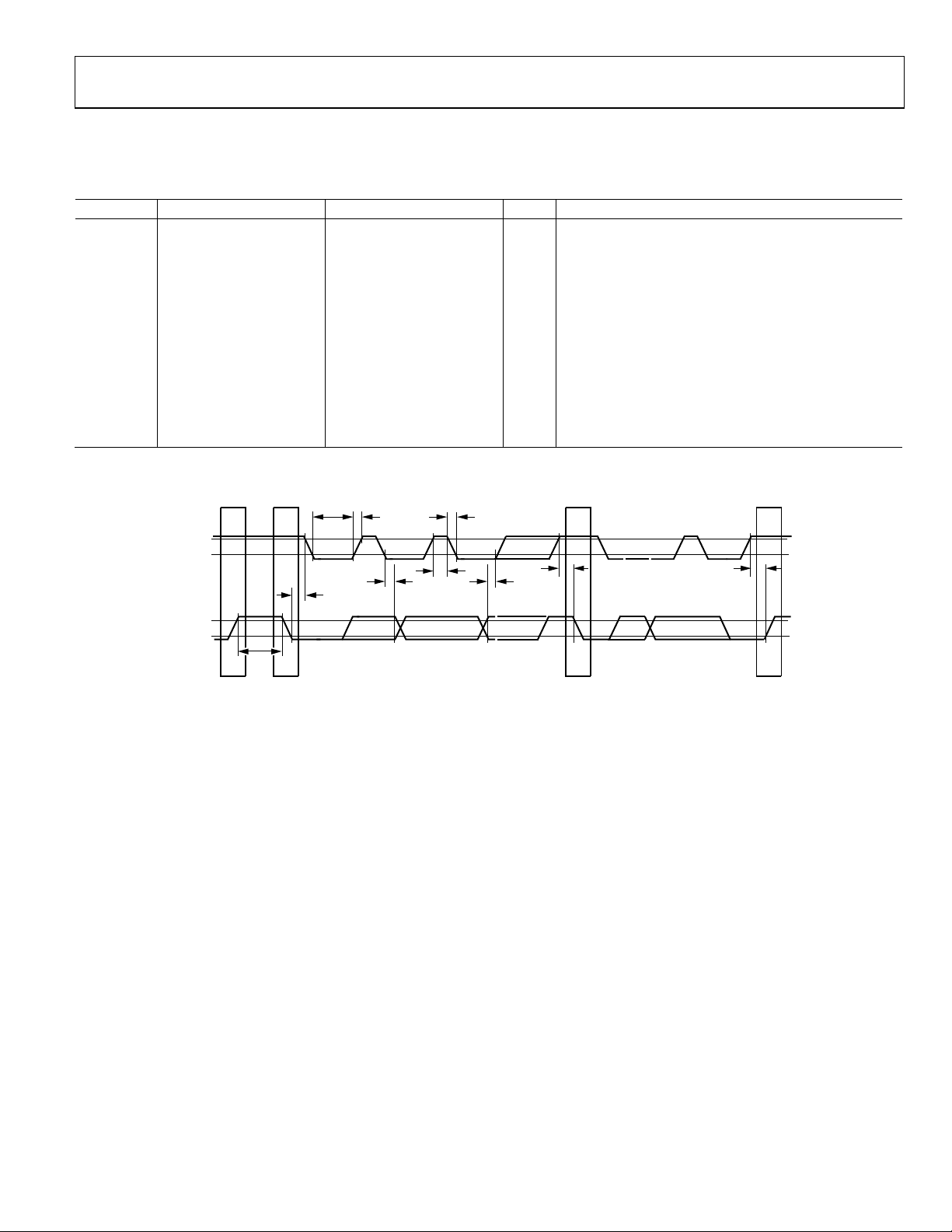
SERIAL BUS TIMING CHARACTERISTICS
tR = (V
Table 2.
Parameter Description Min Ty p Max Unit Test Conditions/Comments
f
Clock frequency 400 kHz
SCLK
t
Bus free time 1.3 µs Following the stop condition of a read transaction
BUF
4.7 µs Following the stop condition of a write transaction
t
HD ;STA
t
SU;STA
t
SU;STO
t
HD ;D AT
t
SU ;D AT
t
SCL low time 1.3 µs
LOW
t
SCL high time 0.6 µs
HIGH
tR SCL, SDA rise time 20 300 ns
tF SCL, SDA fall time 20 300 ns
Timing Diagram
IL(MAX )
– 0.15) to (V
+ 0.15) and tF = 0.9VDD to (V
IH3V3
– 0.15); where V
IL(MAX)
Start hold time 0.6 µs
Start setup time 0.6 µs
Stop setup time 0.6 µs
SDA hold time 300 900 ns
SDA setup time 100 ns
= 2.1 V and VDD = 3.3 V.
IH3V3
Figure 2. Serial Bus Timing Diagram
Rev. B | Page 7 of 48
Page 8
ADM1275
ABSOLUTE MAXIMUM RATINGS
Table 3.
Parameter Rating
VCC Pin −0.3 V to +25 V
UV Pin −0.3 V to +4 V
OV Pin −0.3 V to +4 V
SS Pin −0.3 V to VCAP + 0.3 V
TIMER Pin −0.3 V to VCAP + 0.3 V
VCAP Pin −0.3 V to +4 V
ISET Pin −0.3 V to VCAP + 0.3 V
LATCH Pin
−0.3 V to +25 V
SCL Pin −0.3 V to +6.5 V
SDA Pin −0.3 V to +6.5 V
ADR Pin −0.3 V to VCAP + 0.3 V
GPO1/ALERT1/CONV Pin, ENABLE Pin
GPO2/ALERT2 Pin
−0.3 V to +25 V
−0.3 V to +25 V
PWRGD Pin −0.3 V to +25 V
FLB Pin −0.3 V to +25 V
VOUT Pin −0.3 V to +25 V
GATE Pin (Internal Supply Only)1 −0.3 V to +36 V
SENSE+ Pin −0.3 V to +25 V
SENSE− Pin −0.3 V to +25 V
V
(V
SENSE
SENSE+
− V
) ±0.3 V
SENSE−
Continuous Current into Any Pin ±10 mA
Storage Temperature Range −65°C to +125°C
Operating Temperature Range −40°C to +85°C
Lead Temperature, Soldering (10 sec) 300°C
Junction Temperature 150°C
1
The GATE pin has internal clamping circuits to prevent the GATE pin voltage
from exceeding the maximum ratings of a MOSFET with V
internal process limits. Applying a voltage source to this pin externally may
cause irreversible damage.
= 20 V and
GSMAX
Stresses above those listed under Absolute Maximum Ratings
may cause permanent damage to the device. This is a stress
rating only; functional operation of the device at these or any
other conditions above those indicated in the operational
section of this specification is not implied. Exposure to absolute
maximum rating conditions for extended periods may affect
device reliability.
THERMAL CHARACTERISTICS
θJA is specified for the worst-case conditions, that is, a device
soldered in a circuit board for surface-mount packages.
Table 4. Thermal Resistance
Package Type θJA Unit
16-lead QSOP (RQ-16) 150 °C/W
20-lead QSOP (RQ-20) 126 °C/W
20-lead LFCSP (CP-20-9) 30.4 °C/W
ESD CAUTION
Rev. B | Page 8 of 48
Page 9
ADM1275
1
2
3
4
5
6
7
8
9
10
20
19
18
17
16
15
14
13
12
11
UV
OV
VCAP
TIMER
SS
ISET
VCC
SENSE–
GATE
GND
PWRGD
FLB
VOUT
GPO1/ALERT1/CONV
ADR
LATCH
GPO2/ALERT2
SDA
SCL
SENSE+
ADM1275-1
TOP VIEW
(Not to S cale)
08931-006
1OV
2VCAP
3ISET
4SS
5TIMER
NOTES
1. SOLDER THE EXPOSED PADDLE TO
THE BOARD TO IMPROVE THERMAL
DISSIPATION. THE EXPOSED PADDLE
CAN BE CONNECTED TO GROUND.
LATCH
ADR
GPO1/ALERT1/CONV
GPO2/ALERT2
SDA
13
14
15
12
11
FLB
VOUT
GND
PWRGD
SCL
SENSE+
VCC
UV
SENSE–
GATE
6
7
8
01
9
81
91
02
71
61
08931-109
ADM1275-1
TOP VIEW
(Not to S cale)
PIN 1
INDICATOR
PIN CONFIGURATIONS AND FUNCTION DESCRIPTIONS
Figure 3. ADM1275-1 Pin Configuration, QSOP
Figure 4. ADM1275-1 Pin Configuration, LFCSP
Table 5. ADM1275-1 Pin Function Descriptions
Pin No.
QSOP LFCSP Mnemonic Description
1 19 VCC Positive Supply Input Pin. An undervoltage lockout (UVLO) circuit resets the device when a low
2 20 UV Undervoltage Input Pin. An external resistor divider is used from the supply to this pin to allow an
3 1 OV Overvoltage Input Pin. An external resistor divider is used from the supply to this pin to allow an
4 2 VCAP Internal Regulated Supply. A capacitor with a value of 1 µF or greater should be placed on this pin
5 3 ISET This pin allows the current limit threshold to be programmed. The default limit is set when this pin
6 4 SS Soft Start Pin. A capacitor is used on this pin to set the soft start ramp profile. The voltage on the
7 5 TIMER Timer Pin. An external capacitor, C
8 6
9 7 ADR PMBus Address Pin. This pin can be tied to GND, tied to VCAP, left floating, or tied low through a
10 8 GPO1/
11 9 GPO2/
LATC H
CONV
supply voltage is detected. GATE is held low when the supply is below UVLO. During normal
operation, this pin should remain greater than or equal to SENSE+ to ensure that specifications
are adhered to. No sequencing is required.
internal comparator to detect whether the supply is under the UV limit.
internal comparator to detect whether the supply is above the OV limit.
to maintain good accuracy. This pin can be used as a reference to program the ISET pin voltage.
is connected directly to VCAP. To achieve a user-defined sense voltage, the current limit can be
adjusted using a resistor divider from VCAP. An external reference can also be used.
SS pin controls the current sense voltage limit, which controls the inrush current profile.
, sets an initial timing cycle delay and a fault delay. The GATE
TIMER
pin is pulled low when the voltage on the TIMER pin exceeds the upper threshold.
Signals that the device is latching off after an overcurrent fault. The device can be configured for
automatic retry after latch-off by connecting this pin directly back to the UV pin.
resistor to set four different PMBus addresses (see the Device Addressing section).
/
ALERT1
General-Purpose Digital Output (GPO1).
Alert (
). This pin can be configured to generate an alert signal when one or more fault or
ALERT1
warning conditions are detected.
Conversion (CONV). This pin can be used as an input signal to control when a power monitor ADC
sampling cycle begins.
At power-up, this pin defaults to a high impedance state. There is no internal pull-up on this pin.
General-Purpose Digital Output (GPO2).
ALERT2
Alert (
). This pin can be configured to generate an alert signal when one or more fault or
ALERT2
warning conditions are detected.
At power-up, this pin indicates the FET health mode by default. There is no internal pull-up on this pin.
Rev. B | Page 9 of 48
Page 10

ADM1275
Pin No.
QSOP LFCSP Mnemonic Description
12 10 SDA Serial Data Input/Output Pin. Open-drain input/output. Requires an external resistive pull-up.
13 11 SCL Serial Clock Pin. Open-drain input. Requires an external resistive pull-up.
14 12 PWRGD Power-Good Signal. Used to indicate that the supply is within tolerance. This signal is based on the
voltage present on the FLB pin.
15 13 FLB Foldback Pin. A foldback resistor divider is placed from the source of the FET to this pin. Foldback is
used to reduce the current limit when the source voltage drops. The foldback feature ensures that
the power through the FET is not increased beyond the SOA limits.
16 14 VOUT This pin is used to read back the output voltage using the internal ADC. A 1 kΩ resistor should be
inserted in series between the source of a FET and the VOUT pin.
17 15 GND Chip Ground Pin.
18 16 GAT E Gate Output Pin. This pin is the high-side gate drive of an external N-channel FET. This pin is driven
by the FET drive controller, which uses a charge pump to provide a pull-up current to charge the FET
gate pin. The FET drive controller regulates to a maximum load current by regulating the GATE pin.
GATE is held low when the supply is below UVLO.
19 17 SENSE− Negative Current Sense Input Pin. A sense resistor between the SENSE+ pin and the SENSE− pin sets
the analog current limit. The hot-swap operation of the ADM1275 controls the external FET gate to
maintain the sense voltage (V
20 18 SENSE+ Positive Current Sense Input Pin. This pin connects to the main supply input. A sense resistor
between the SENSE+ pin and the SENSE− pin sets the analog current limit. The hot-swap operation
of the ADM1275 controls the external FET gate to maintain the sense voltage (V
pin is also used to measure the supply input voltage using the ADC.
N/A EP EPAD Exposed Paddle on Underside of LFCSP. Solder the exposed paddle to the board to improve thermal
dissipation. The exposed paddle can be connected to ground.
SENSE+
− V
). This pin also connects to the FET drain pin.
SENSE−
SENSE+
− V
SENSE−
). This
Rev. B | Page 10 of 48
Page 11
ADM1275
1
2
3
4
5
6
7
8
16
15
14
13
12
11
10
9
UV
VCAP
ISET
ADR
TIMER
SS
VCC
SENSE–
GATE
GND
SCL
GPO1/ALERT1/CONV SDA
PWRGD
FLB
SENSE+
ADM1275-2
TOP VIEW
(Not to S cale)
08931-007
Foldback Pin. A foldback resistor divider is placed from the source of the FET to this pin. Foldback
Figure 5. ADM1275-2 Pin Configuration
Table 6. ADM1275-2 Pin Function Descriptions
Pin No. Mnemonic Description
1 VCC Positive Supply Input Pin. An undervoltage lockout (UVLO) circuit resets the device when a low
supply voltage is detected. GATE is held low when the supply is below UVLO. During normal
operation, this pin should remain greater than or equal to SENSE+ to ensure that specifications
are adhered to. No sequencing is required.
2 UV Undervoltage Input Pin. An external resistor divider is used from the supply to this pin to allow
an internal comparator to detect whether the supply is under the UV limit.
3 VCAP Internal Regulated Supply. A capacitor with a value of 1 µF or greater should be placed on this pin
to maintain good accuracy. This pin can be used as a reference to program the ISET pin voltage.
4 ISET This pin allows the current limit threshold to be programmed. The default limit is set when this
pin is connected directly to VCAP. To achieve a user-defined sense voltage, the current limit can
be adjusted using a resistor divider from VCAP. An external reference can also be used.
5 SS Soft Start Pin. A capacitor is used on this pin to set the soft start ramp profile. The voltage on the
SS pin controls the current sense voltage limit, which controls the inrush current profile.
6 TIMER Timer Pin. An external capacitor, C
TIMER
GAT E pin is pulled low when the voltage on the TIMER pin exceeds the upper threshold.
7 ADR PMBus Address Pin. This pin can be tied to GND, tied to VCAP, left floating, or tied low through a
resistor to set four different PMBus addresses (see the Device Addressing section).
8 GPO1/
/CONV General-Purpose Digital Output (GPO1).
ALERT1
Alert (
). This pin can be configured to generate an alert signal when one or more fault or
ALERT1
warning conditions are detected.
Conversion (CONV). This pin can be used as an input signal to control when a power monitor
ADC sampling cycle begins.
At power-up, this pin defaults to a high impedance state. There is no internal pull-up on this pin.
9 SDA Serial Data Input/Output Pin. Open-drain input/output. Requires an external resistive pull-up.
10 SCL Serial Clock Pin. Open-drain input. Requires an external resistive pull-up.
11 PWRGD Power-Good Signal. Used to indicate that the supply is within tolerance. This signal is based on
the voltage present on the FLB pin.
12 FLB
is used to reduce the current limit when the source voltage drops. The foldback feature ensures
that the power through the FET is not increased beyond the SOA limits.
13 GND Chip Ground Pin.
14 GATE Gate Output Pin. This pin is the high-side gate drive of an external N-channel FET. This pin is
driven by the FET drive controller, which uses a charge pump to provide a pull-up current to
charge the FET gate pin. The FET drive controller regulates to a maximum load current by
regulating the GATE pin. GATE is held low when the supply is below UVLO.
15 SENSE− Negative Current Sense Input Pin. A sense resistor between the SENSE+ pin and the SENSE− pin
sets the analog current limit. The hot-swap operation of the ADM1275 controls the external FET
gate to maintain the sense voltage (V
16 SENSE+ Positive Current Sense Input Pin. This pin connects to the main supply input. A sense resistor
between the SENSE+ pin and the SENSE− pin sets the analog current limit. The hot-swap operation
of the ADM1275 controls the external FET gate to maintain the sense voltage (V
This pin is also used to measure the supply input voltage using the ADC.
Rev. B | Page 11 of 48
, sets an initial timing cycle delay and a fault delay. The
SENSE+
− V
). This pin also connects to the FET drain pin.
SENSE−
SENSE+
− V
SENSE−
).
Page 12
ADM1275
1
2
3
4
5
6
7
8
9
1
0
20
19
18
17
16
15
14
13
12
11
UV
OV
VCAP
TIMER
SS
ISET
VCC
SENSE–
GATE
GND
PWRGD
FLB
VOUT
ENABLE
ADR
LATCH
GPO2/ALERT2
SDA
SCL
SENSE+
ADM1275-3
TOP VIEW
(Not to S cale)
08931-008
1OV
2VCAP
3ISET
4SS
5TIMER
LATCH
ADR
ENABLE
GPO2/ALERT2
SDA
13
14
15
12
11
FLB
VOUT
GND
PWRGD
SCL
SENSE+
VCC
UV
SENSE–
GATE
6
7
8
01
9
81
91
02
71
61
08931-110
ADM1275-3
TOP VIEW
(Not to S cale)
PIN 1
INDICATOR
NOTES
1. SOLDER THE EXPOSED PADDLE TO
THE BOARD TO IMPROVE THERMAL
DISSIPATION. THE EXPOSED PADDLE
CAN BE CONNECTED TO GROUND.
Figure 6. ADM1275-3 Pin Configuration, QSOP
Table 7. ADM1275-3 Pin Function Descriptions
Pin No.
QSOP LFCSP Mnemonic Description
1 19 VCC Positive Supply Input Pin. An undervoltage lockout (UVLO) circuit resets the device when a low
2 20 UV Undervoltage Input Pin. An external resistor divider is used from the supply to this pin to allow an
3 1 OV Overvoltage Input Pin. An external resistor divider is used from the supply to this pin to allow an
4 2 VCAP Internal Regulated Supply. A capacitor with a value of 1 µF or greater should be placed on this pin
5 3 ISET This pin allows the current limit threshold to be programmed. The default limit is set when this pin
6 4 SS Soft Start Pin. A capacitor is used on this pin to set the soft start ramp profile. The voltage on the
7 5 TIMER Timer Pin. An external capacitor, C
8 6
9 7 ADR PMBus Address Pin. This pin can be tied to GND, tied to VCAP, left floating, or tied low through a
10 8 ENABLE Digital Logic Input. This input must be high to allow the ADM1275-3 hot-swap controller to begin a
11 9 GPO2/
12 10 SDA Serial Data Input/Output Pin. Open-drain input/output. Requires an external resistive pull-up.
13 11 SCL Serial Clock Pin. Open-drain input. Requires an external resistive pull-up.
14 12 PWRGD Power-Good Signal. Used to indicate that the supply is within tolerance. This signal is based on the
15 13 FLB Foldback Pin. A foldback resistor divider is placed from the source of the FET to this pin. Foldback is
Figure 7. ADM1275-3 Pin Configuration, LFCSP
supply voltage is detected. GATE is held low when the supply is below UVLO. During normal
operation, this pin should remain greater than or equal to SENSE+ to ensure that specifications are
adhered to. No sequencing is required.
internal comparator to detect whether the supply is under the UV limit.
internal comparator to detect whether the supply is above the OV limit.
to maintain good accuracy. This pin can be used as a reference to program the ISET pin voltage.
is connected directly to VCAP. To achieve a user-defined sense voltage, the current limit can be
adjusted using a resistor divider from VCAP. An external reference can also be used.
SS pin controls the current sense voltage limit, which controls the inrush current profile.
, sets an initial timing cycle delay and a fault delay. The GATE
TIMER
pin is pulled low when the voltage on the TIMER pin exceeds the upper threshold.
Signals that the device is latching off after an overcurrent fault. The device can be configured for
LATC H
automatic retry after latch-off by connecting this pin directly back to the UV pin.
resistor to set four different PMBus addresses (see the Device Addressing section).
power-up sequence. If this pin is held low, the ADM1275-3 is prevented from powering up. There is
no internal pull-up on this pin.
General-Purpose Digital Output (GPO2).
ALERT2
Alert (
). This pin can be configured to generate an alert signal when one or more fault or
ALERT2
warning conditions are detected.
At power-up, this pin indicates the FET health mode by default. There is no internal pull-up on this pin.
voltage present on the FLB pin.
used to reduce the current limit when the source voltage drops. The foldback feature ensures that
the power through the FET is not increased beyond the SOA limits.
Rev. B | Page 12 of 48
Page 13

ADM1275
Pin No.
QSOP LFCSP Mnemonic Description
16 14 VOUT This pin is used to read back the output voltage using the internal ADC. A 1 kΩ resistor should be
inserted in series between the source of a FET and the VOUT pin.
17 15 GND Chip Ground Pin.
18 16 GATE Gate Output Pin. This pin is the high-side gate drive of an external N-channel FET. This pin is driven
by the FET drive controller, which uses a charge pump to provide a pull-up current to charge the FET
gate pin. The FET drive controller regulates to a maximum load current by regulating the GATE pin.
GATE is held low when the supply is below UVLO.
19 17 SENSE− Negative Current Sense Input Pin. A sense resistor between the SENSE+ pin and the SENSE− pin sets
the analog current limit. The hot-swap operation of the ADM1275 controls the external FET gate to
maintain the sense voltage (V
SENSE+
− V
20 18 SENSE+ Positive Current Sense Input Pin. This pin connects to the main supply input. A sense resistor
between the SENSE+ pin and the SENSE− pin sets the analog current limit. The hot-swap operation
of the ADM1275 controls the external FET gate to maintain the sense voltage (V
pin is also used to measure the supply input voltage using the ADC.
N/A EP EPAD Exposed Paddle on Underside of LFCSP. Solder the exposed paddle to the board to improve thermal
dissipation. The exposed paddle can be connected to ground.
). This pin also connects to the FET drain pin.
SENSE−
SENSE+
− V
SENSE−
). This
Rev. B | Page 13 of 48
Page 14
ADM1275
0
1
2
3
4
5
I
CC
(mA)
VCC (V)
2 4 6 8 10 12 14 16 18
20
08931-009
+25°C
+85°C
–40°C
0
1
2
3
4
5
–40 –20 0
I
CC
(mA)
TEMPERATURE (°C)
VCC = 20V
VCC = 12V
V
CC
= 2.95V
08931-010
20 40
60 80
0
2
4
6
8
10
12
14
2 4 6 8 1210 14 16 18 20
I
GATEDN_SLOW
(mA)
VCC (V)
08931-011
+25°C
–40°C
+85°C
0
2
4
6
8
10
12
14
I
GATEDN_SLOW
(mA)
TEMPERATURE (°C)
08931-012
V
CC
= 12V
–40
–20 0 20 40 60 80
0
1
2
3
4
5
6
7
8
9
10
11
12
13
14
15
0 5 10 15 20 25
I
GATEDN_SLOW
(mA)
V
GATE
(V)
08931-013
–40
–35
–30
–25
–20
–15
–10
–5
0
2 4 6 8 10 12 14 16 18 20
I
GATEUP
(µA)
VCC (V)
08931-014
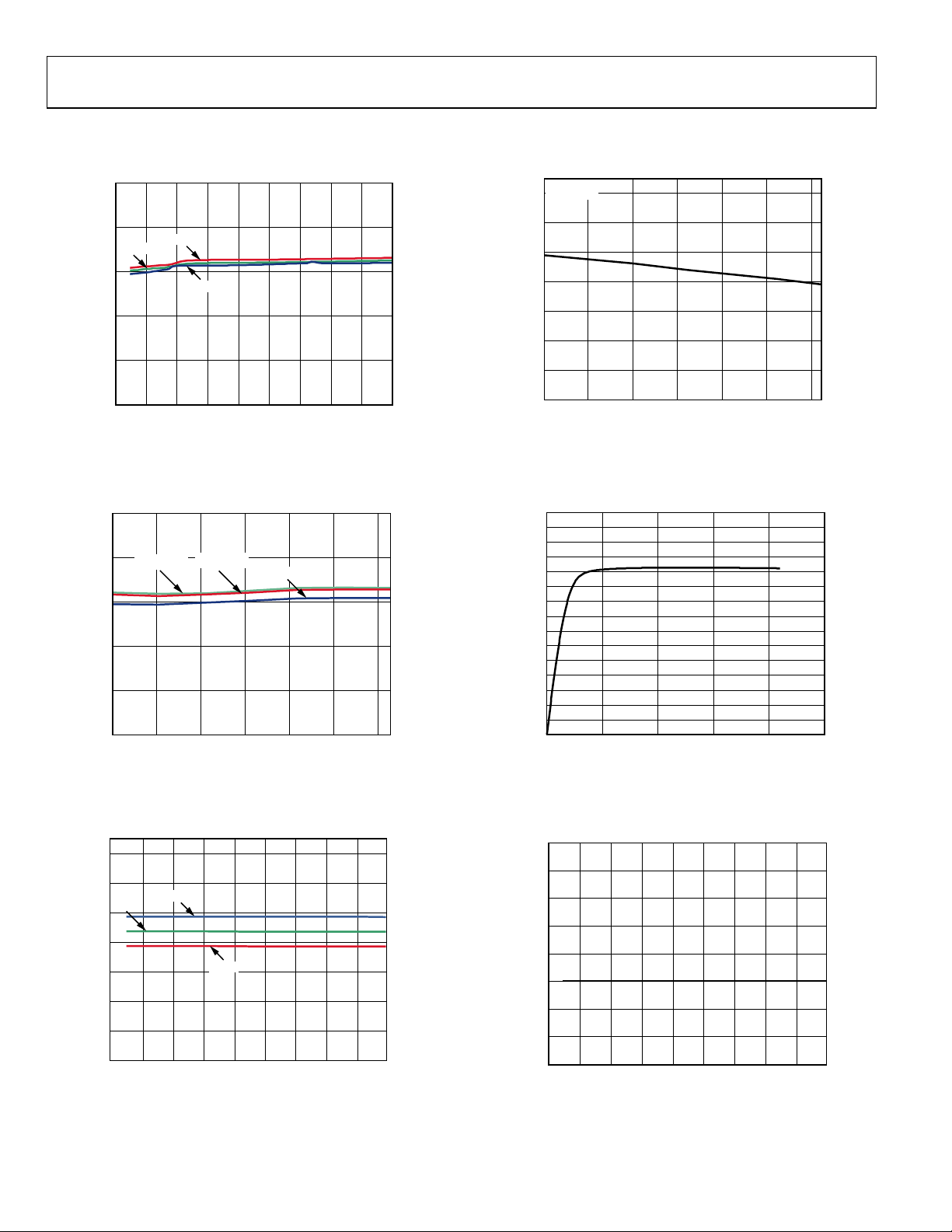
TYPICAL PERFORMANCE CHARACTERISTICS
Figure 8. Supply Current (ICC) vs. Supply Voltage (VCC)
Figure 11. Gate Pull-Down Current (I
GATEDN_SLOW
) vs. Temperature
Figure 9. Supply Current (I
Figure 10. Gate Pull-Down Current (I
GATEDN_SLOW
) vs. Temperature
CC
) vs. Supply Voltage (VCC)
Figure 12. Gate Pull-Down Current (I
GATEDN_S LOW
) vs. Gate Voltage (V
GATE
)
Figure 13. Gate Pull-Up Current (I
) vs. Supply Voltage (VCC)
GATEUP
Rev. B | Page 14 of 48
Page 15
ADM1275
0
5
10
15
20
25
30
0 5 10 15 20 25
I
GATEUP
(µA)
V
GATE
(V)
VCC = 12V
V
CC
= 2.95V
08931-016
–40
–35
–30
–25
–20
–15
–10
–5
0
I
GATEUP
(µA)
TEMPERATURE (°C)
V
CC
= 12V
08931-015
–40
–20 0 20 40 60 80
0
2
4
6
8
10
12
14
16
2 20
ΔV
GATE
(V)
V
CC
(V)
+85°C
+25°C
–40°C
08931-017
4 6 8 10 12 14 16 18
0
2
4
6
8
10
12
14
16
ΔV
GATE
(V)
V
CC
(V)
08931-018
2 4 6 8 10 12 14 16 18 20
+25°C
+85°C
–40°C
0
2
4
6
8
10
12
14
16
–40 –20 0 20 40 60
ΔV
GATE
(V)
TEMPERATURE (°C)
V
CC
= 12V
V
CC
= 20V
V
CC
= 2.95V
08931-019
80
–20
–18
–16
–14
–12
–10
–8
–6
–4
–2
0
–40
I
SS
PULL-UP (µA)
TEMPERATURE (°C)
V
CC
= 12V
08931-020
–20 0 20 40 60 80
Figure 14. Gate Pull-Up Current (I
Figure 15. Gate Pull-Up Current (I
) vs. Gate Voltage (V
GATEUP
) vs. Temperature
GATEUP
GATE
)
Figure 17. Gate Drive Voltage (ΔV
Figure 18. Gate Drive Voltage (ΔV
) vs. Supply Voltage (VCC), 5 µA Load
GATE
) vs. Temperature, No Load
GATE
Figure 16. Gate Drive Voltage (ΔV
) vs. Supply Voltage (VCC), No Load
GATE
Rev. B | Page 15 of 48
Figure 19. Soft Start Pull-Up Current (I
) vs. Temperature
SS
Page 16

ADM1275
–80
–70
–60
–50
–40
–30
–20
–10
0
I
TIMERUPFLT
(µA)
–40
TEMPERATURE (°C)
08931-021
–20 0 20 40 60 80
VCC = 12V
–20 0 20 40 60 80
–10
–8
–6
–4
–2
0
I
TIMERUPPOR
(µA)
–40
TEMPERATURE (°C)
V
CC
= 12V
08931-022
–40
–20 0 20 40 60
80
0
1.5
3.0
4.5
I
TIMERDNRT
(µA)
V
CC
= 12V
TEMPERATURE (°C)
08931-023
0
100
200
300
400
500
600
700
800
900
1000
1100
TIMER T HRE S HOLD (mV)
–40
TEMPERATURE (°C)
08931-024
–20 0 20 40
60 80
LOW THRESHOLD (V
CC
= 12V)
HIGH THRES HOLD (V
CC
= 12V)
–40 –20 0
TEMPERATURE (°C)
20 40 60 80
0
0.1
0.2
0.3
0.4
0.5
0.6
0.7
0.8
0.9
1.0
1.1
1.2
1.3
FOLDBACK T HRE S HOLD (V)
2.95V
12V
20V
08931-025
0
0.5
1.0
1.5
2.0
2.5
3.0
FOLDBACK HYS TERESIS CURRENT (µA)
08931-026
2.95V
12V
20V
–40 –20 0
TEMPERATURE (°C)
20 40 60 80
Figure 20. Timer Pull-Up Current, Overcurrent Fault (I
vs. Temperature
Figure 21. Timer Pull-Up Current, Power-On Reset (I
vs. Temperature
TIMERUPFL T
TIMERUPPOR
)
)
Figure 23. Timer Thresholds vs. Temperature
Figure 24. Foldback Threshold vs. Temperature
Figure 22. Timer Pull-Down Current, Retry (I
vs. Temperature
TIMERDNRT
)
Figure 25. Foldback Hysteresis Current vs. Temperature
Rev. B | Page 16 of 48
Page 17

ADM1275
0
20
40
60
80
100
120
140
160
180
200
220
240
FOLDBACK CL AMP (mV)
TEMPERATURE (°C)
08931-027
VCC = 12V
–40
–20 0 20 40 60 80
0
25
50
75
100
125
150
175
200
225
250
275
300
325
350
375
400
2 20
OC RESPONSE TIME (ns)
VCC (V)
08931-128
4 6 8 10 12 14 16 18
+85°C
–40°C
+25°C
0
25
50
75
100
125
150
175
200
225
250
275
300
325
350
375
400
OC RESPONSE TIME (ns)
VCC (V)
08931-129
2 20
4 6 8 10 12 14 16 18
+85°C
+25°C
–40°C
0
0.2
0.4
0.6
0.8
1.0
1.2
1.4
1.6
1.8
2.0
2 20
V
CBOS
(mV)
VCC (V)
–40°C
08931-130
+85°C
+25°C
4 6 8 10 12 14 16 18
0
5
10
15
20
25
30
V
SENSECL
(mV)
TEMPERATURE (°C)
–40
08931-131
–20 0 20 40 60 80
V
CC
= 12V
0
5
10
15
20
25
30
1.11.00.90.80.70.60.50.40.30.20.10
V
SENSECL
(mV)
V
FLB
(V)
T
A
= 25°C
08931-132
Figure 26. Foldback Clamp vs. Temperature
Figure 29. Circuit Breaker Offset (V
) vs. Supply Voltage (VCC)
CBOS
Figure 27. Severe Overcurrent Response Time vs. Supply Voltage (VCC),
V
ISET
Figure 28. Severe Overcurrent Response Time vs. Supply Voltage (VCC),
V
= 0.25 V
= 1 V
ISET
Figure 30. Hot-Swap Sense Voltage Current Limit (V
SENSECL
)
vs. Temperature
Figure 31. Hot-Swap Sense Voltage Current Limit (V
vs. Foldback Voltage (V
)
FLB
SENSECL
)
Rev. B | Page 17 of 48
Page 18

ADM1275
0
5
10
15
20
25
30
35
40
45
50
V
SENSEOC
(mV)
VCC (V)
08931-133
T
A
= 25°C
2 4 6 8 10 12 14 16 18 20
15
10
5
0
20
25
30
35
40
45
50
V
SENSEOC
(mV)
VCC = 12V
TEMPERATURE (°C)
08931-144
–40 –20 0 20 40 60 80
0 1 2 3 4 5 6 7 8 9 10 11 12
0
50
100
150
08931-134
I
SENSEx
(µA)
V
SENSEx
(V)
0
5
10
15
20
0 –2 –4 –6 –8 –10 –12 –14 –16 –18 –20 –22 –24 –26
ΔV
GATE
(V)
I
GATEUP
(µA)
V
CC
= 2.95V
VCC = 12V
VCC = 20V
08931-135
0
0.2
0.4
0.6
0.8
1.0
1.2
1.4
1.6
1.8
2.0
0 1 2 3 4 5 6 7 8 9 10
V
OL_PWRGD
(V)
I
OL
(mA)
V
CC
= 2.95V
VCC = 12V
08931-136
0
0.2
0.4
0.6
0.8
1.0
1.2
1.4
1.6
1.8
2.0
V
OL
(V)
V
CC
= 2.95V
V
CC
= 12V
08931-137
0 1 2 3 4 5 6 7 8 9 10
I
OL
(mA)
Figure 32. Severe Overcurrent Voltage Threshold (V
vs. Supply Voltage (V
), V
= V
CC
ISET
VCAP
Figure 33. Severe Overcurrent Voltage Threshold (V
vs. Temperature, V
ISET
= V
VCAP
SENSEOC
SENSEOC
)
)
Figure 35. Gate Drive Voltage (ΔV
Figure 36. PWRGD Pin, V
) vs. Gate Pull-Up Current (I
GATE
vs. IOL
OL_PWRGD
GATEUP
)
Figure 34. SENSE+/SENSE− Input Current (I
SENSEx
) vs. Voltage (V
)
SENSEx
Rev. B | Page 18 of 48
Figure 37.
LATCH
and GPOx/
ALERTx
Digital Outputs, VOL vs. IOL
Page 19

ADM1275
0
0.5
1.0
1.5
2.0
2.5
3.0
0 50 100
V
VCAP
(V)
I
VCAP
(µA)
+85°C
+25°C
–40°C
08931-138
0
100
200
300
400
500
600
700
800
900
1000
1100
1200
–40 –20 20 40 600 80
UV THRESHOLD (mV)
TEMPERATURE (°C)
V
CC
= 12V
08931-139
–40
TEMPERATURE (°C)
0
100
200
300
400
500
600
700
800
900
1000
1100
1200
OV THRESHOLD (mV)
VCC = 12V
08931-140
–20 20 40 600 80
0
0.5
1.0
1.5
2.0
2.5
3.0
–25 –20 –15 –10 –5 0 5
V
ADR
(V)
I
ADR
(µA)
00 DECODE 01 DECODE 10 DECODE
11 DECODE
08931-141
08931-142
0
1
2
3
4
5
6
7
8
9
10
0 5 10 15 20 25 30
ACCURACY (%)
SENSE VOLTAGE (mV)
16× AVERAGING
128× AVERAGING
Figure 38. VCAP Voltage (V
) vs. VCAP Load (I
VCAP
VCAP
)
Figure 41. ADR Pin Voltage (V
) vs. Current (I
ADR
ADR
)
Figure 39. UV Threshold (UV
Figure 40. OV Threshold (OV
) vs. Temperature
TH
) vs. Temperature
TH
Figure 42. Worst-Case Current Sense Power Monitor Error vs. Current Sense
Voltage (V
), 0°C to 65°C, V
SENSE
SENSE+
= 12 V
Rev. B | Page 19 of 48
Page 20

ADM1275
GATE
SENSE+
TIMER
TIMER
ADM1275-1
GND
SENSE–
VCC
V
CP
×50
+
–
VCAP
IOUT
UV
OV
1.0V
1.0V
VOUT
VOUT
SCL
SDA
ADR
SENSE+
IOUT
LDO
CHARGE
PUMP
TIMEOUT
GPO2/ALERT2
PWRGD
GPO1/ALERT1/CONV
LATCH
CURRENT
LIMIT
SS
CURRENT
LIMIT
FLB
ISET
TIMEOUT
CURRENT
LIMIT
CONTROL
REF
SELECT
1.0V
GATE
DRIVE/
LOGIC
LOGIC
AND
PMBus
–
+
–
+
–
+
08931-003
12-BIT
ADC
GATE
SENSE+
TIMER
TIMER
ADM1275-2
GND
SENSE–
VCC
V
CP
VCAP
IOUT
UV
1.0V
VOUT
SCL
SDA
ADR
SENSE+
IOUT
LDO
CHARGE
PUMP
TIMEOUT
PWRGD
GPO1/ALERT1/CONV
CURRENT
LIMIT
SS
CURRENT
LIMIT
FLB
ISET
TIMEOUT
CURRENT
LIMIT
CONTROL
REF
SELECT
1.0V
GATE
DRIVE/
LOGIC
LOGIC
AND
PMBus
×50
+
+
–
–
+
–
08931-004
12-BIT
ADC
GATE
SENSE+
TIMER
TIMER
ADM1275-3
GND
SENSE–
VCC
V
CP
VCAP
ENABLE
IOUT
UV
OV
1.0V
1.0V
VOUT
VOUT
12-BIT
ADC
SCL
SDA
ADR
SENSE+
IOUT
LDO
CHARGE
PUMP
TIMEOUT
GPO2/ALERT2
PWRGD
LATCH
CURRENT
LIMIT
SS
CURRENT
LIMIT
FLB
ISET
TIMEOUT
CURRENT
LIMIT
CONTROL
REF
SELECT
1.0V
GATE
DRIVE/
LOGIC
LOGIC
AND
PMBus
×50
+
+
+
+
–
–
–
–
08931-005
FUNCTIONAL BLOCK DIAGRAMS
Figure 43. ADM1275-1 Functional Block Diagram
Figure 44. ADM1275-2 Functional Block Diagram
Figure 45. ADM1275-3 Functional Block Diagram
Rev. B | Page 20 of 48
Page 21

ADM1275
2.95V TO 20V
R
SENSE
Q
1
SENSE–
GND
GATE
VCC
SENSE+
ADM1275
08931-028
2.95V TO 20V
R
SENSE
Q
1
SENSE–
GND
GATE
VCC
330nF
SENSE+
22Ω
ADM1275
08931-029
R
SENSE
Q
1
SENSE–
GND
GATE
VCC
SENSE+
ADM1275
OVERCURRENT
REFERENCE
×50
08931-030
+
+––
THEORY OF OPERATION
When circuit boards are inserted into a live backplane, discharged
supply bypass capacitors draw large transient currents from the
backplane power bus as they charge. These transient currents can
cause permanent damage to connector pins, as well as dips on
the backplane supply that can reset other boards in the system.
The ADM1275 is designed to control the powering on and
off of a system in a controlled manner, allowing a board to be
removed from, or inserted into, a live backplane by protecting
it from excess currents. The ADM1275 can reside on the backplane or on the removable board.
POWERING THE ADM1275
A supply voltage from 2.95 V to 20 V is required to power the
ADM1275 via the VCC pin. The VCC pin provides the majority
of the bias current for the device; the remainder of the current
needed to control the gate drive and best regulate the V
voltage is supplied by the SENSE+ pin.
To ensure correct operation of the ADM1275, the voltage on
the VCC pin must be greater than or equal to the voltage on
the SENSE+ pin. No sequencing of the VCC and SENSE+ rails
is necessary. The SENSE+ pin can be as low as 2 V for normal
operation provided that a voltage of at least 2.95 V is connected
to the VCC pin. In most applications, both the VCC and
SENSE+ pins are connected to the same voltage rail, but they
are connected via separate traces to prevent accuracy loss in the
sense voltage measurement (see Figure 46).
Figure 46. Powering the ADM1275
To protect the ADM1275 from unnecessary resets due to transient
supply glitches, an external resistor and capacitor can be added,
as shown in Figure 47. The values of these components should be
chosen to provide a time constant that can filter any expected
glitches. The resistor should, however, be small enough to keep
voltage drops due to quiescent current to a minimum. A supply
decoupling capacitor should not be placed on the rail before the
FET unless a resistor is used to limit the inrush current.
GS
CURRENT SENSE INPUTS
The load current is monitored by measuring the voltage drop
across an external sense resistor, R
internal current sense amplifier provides a gain of 50 to the
voltage drop detected across R
an internal reference and used by the hot-swap control logic to
detect when an overcurrent condition occurs.
The SENSE inputs may be connected to multiple parallel sense
resistors, which can affect the voltage drop detected by the
ADM1275. The current flowing through the sense resistors
creates an offset, resulting in reduced accuracy.
To achieve better accuracy, averaging resistors sum the current
from the nodes of each sense resistor, as shown in Figure 49. The
typical value for the averaging resistors is 10 Ω. The value of the
averaging resistors is chosen to be much greater than the trace
resistance between the sense resistors terminals and the inputs
to the ADM1275. This greatly reduces the effects of differences
in the trace resistances.
Rev. B | Page 21 of 48
Figure 47. Transient Glitch Protection Using an RC Network
(see Figure 48). An
SENSE
. The result is compared to
SENSE
Figure 48. Hot-Swap Current Sense Amplifier
Page 22

ADM1275
Q
1
SENSE–
GND
GATEVCC
SENSE+
BIAS
CURRENT
2.95V
TO 20V
08931-031
R
SENSE
Q
1
SENSE–
GND
GATE
VCC
ISET
SS
FLB
SENSE+
ADM1275
OVERCURRENT
×50
08931-032
SS
FLB
ISET1V
0.2V
0.1V
V
t
CURRENT LIM IT REFERENCE
08931-033
ADM1275
VCAP
ISET
C1
GND
08931-034
Figure 49. Connection of Multiple Sense Resistors to the SENSE Pins
CURRENT LIMIT REFERENCE
The current limit reference voltage determines the load current
level to which the ADM1275 limits the current during an
overcurrent event. This reference voltage is compared to the
gained-up current sense voltage to determine whether the limit
is reached.
An internal current limit reference selector block continuously
compares the ISET, soft start, and foldback voltages to determine
which voltage is the lowest at any given time; the lowest voltage
is used as the current limit reference. This ensures that the
programmed current limit, ISET, is used in normal operation,
and that the soft start and foldback features reduce the current
limit when required during startup and/or fault conditions.
Figure 51. Interaction of Soft Start, Foldback, and ISET Current Limits
SETTING THE CURRENT LIMIT (ISET)
The maximum current limit is partially determined by selecting
a sense resistor to match the current sense voltage limit on the
controller for the desired load current. However, as currents
become larger, the sense resistor requirements become smaller,
and resolution can be difficult to achieve when selecting the
appropriate sense resistor. The ADM1275 provides an adjustable
current sense voltage limit to handle this issue. The device allows
the user to program the required current sense voltage limit
from 5 mV to 25 mV.
The default value of 20 mV is achieved by connecting the ISET
pin directly to the VCAP pin. This configures the device to use
an internal 1 V reference, which equates to 20 mV at the sense
inputs (see Figure 52).
Figure 50. Current Limit Reference Selection
The foldback and soft start voltages vary during different modes
of operation and are, therefore, clamped to minimum levels of
200 mV and 100 m V, respectively, to prevent zero current flow
due to the current limit being too low. Figure 51 provides an
example of how the soft start, foldback, and ISET voltages
interact during startup as the ADM1275 is enhancing the FET
and charging the load capacitances. Depending on how the soft
start and foldback features are configured, the hand-off point
can vary to ensure that the FET is operated correctly.
Figure 52. Fixed 20 mV Current Sense Limit
To program the sense voltage from 5 mV to 25 mV, a resistor
divider is used to set a reference voltage on the ISET pin (see
Figure 53).
Rev. B | Page 22 of 48
Page 23

ADM1275
ADM1275
GND
VCAP
ISET
C1 R1
R2
08931-035
ISET
SS
SS
V
tIC×
=
GATE
SENSE+
ADM1275
GND
SENSE–
×50
SS
CURRENT
LIMIT
FLB
ISET
TIMEOUT
CURRENT
LIMIT
CONTROL
REF
SELECT
1.0V
CURRENT
LIMIT
VCAP
10µA
GATE
DRIVE/
LOGIC
+
+
–
–
08931-036
V
CP
Figure 53. Adjustable 5 mV to 25 mV Current Sense Limit
The VCAP pin has a 2.7 V (±1.5%) internal generated voltage
that can be used to set a voltage at the ISET pin. Assuming that
V
equals the voltage on the ISET pin, the resistor divider
ISET
should be sized to set the ISET voltage as follows:
V
where V
ISET
= V
SENSE
× 50
SENSE
is the current sense voltage limit.
The VCAP rail can also be used as the pull-up supply for setting
2
the I
C address. The VCAP pin should not be used for any other
purpose. To guarantee accuracy specifications, care should be
taken not to load the VCAP pin by more than 100 µA.
SOFT START
A capacitor connected to the SS pin determines the inrush
current profile. Before the FET is enabled, the output voltage of
the current limit reference selector block is clamped at 100 mV.
This, in turn, holds the hot-swap sense voltage current limit,
V
, at approximately 2 mV. When the FET is requested to
SENSECL
turn on, the SS pin is held at ground until the voltage between
the SENSE+ and SENSE− pins (V
breaker voltage, V
V
= V
CB
where V
is typically 0.88 mV, making VCB = 1.12 mV.
CBOS
SENSECL
.
CB
− V
CBOS
When the load current generates a sense voltage equal to V
10 µA current source is enabled, which charges the SS capacitor
and results in a linear ramping voltage on the SS pin. The current
limit reference also ramps up accordingly, allowing the regulated
load current to ramp up while avoiding sudden transients during
power-up. The SS capacitor value is given by
where:
I
= 10 µA.
SS
t = SS ramp time.
For example, a 10 nF capacitor gives a soft start time of 1 ms.
Note that the SS voltage may intersect with the FLB (foldback)
voltage, and the current limit reference may change to follow
FLB (see Figure 51). This change has minimal impact on startup
because the output voltage rises at a similar rate to the SS voltage.
) reaches the circuit
SENSE
Figure 54. Soft Start
FOLDBACK
Foldback is a method to actively reduce the current limit as the
voltage drop across the FET increases. It keeps the power across
the FET to a minimum during power-up, overcurrent, or shortcircuit events. It also avoids the need to oversize the FET to
accommodate worst-case conditions, resulting in board size and
cost savings.
The ADM1275 detects the voltage drop across the FET by
looking at a resistor-divided version of the output voltage. It is
assumed that the supply voltage remains constant and within
tolerance. The device therefore relies on the principle that the
drain of the FET is at the maximum expected supply voltage,
and that the magnitude of the output voltage is relative to that
, a
CB
Rev. B | Page 23 of 48
of the V
voltage to the FLB pin, a relationship from V
to V
The resistor divider should be designed to output a voltage
equal to ISET when V
should be well below the working tolerance of the supply rail.
As V
V
FLB
limit reference selector block. This results in a reduction of the
current limit and, therefore, the regulated load current. To
prevent complete current flow restriction, a clamp becomes
active when the current limit reference reaches 200 m V. T he
current limit cannot drop below this level.
To su it the SOA characteristics of a particular FET, the required
minimum current for this clamp varies from design to design.
However, the current limit reference fixes this clamp at 200 mV,
which equates to 4 mV at the sense resistor. Therefore, the main
ISET voltage can be adjusted to align this clamp to the required
percentage current reduction. For example, if ISET equals 0.8 V,
the clamp can be set at 25% of the maximum current.
of the FET. Using a resistor divider from the output
DS
, and thus VDS,
OUT
can be derived.
FLB
falls below the desired level. This
OUT
continues to drop, the current limit reference follows
OUT
because it is now the lowest voltage input to the current
Page 24

ADM1275
A100
)(
A3 µ
×−
+
µ
×
=
TIMERTIMERLTIMERHTIMERTIMERH
INITIAL
CVVCV
t
TIMER
The TIMER pin handles several timing functions with an
external capacitor, C
V
(0.2 V) and V
TIMERL
sources: a 3 μA pull-up, a 60 μA pull-up, a 2 μA pull-down, and
a 100 μA pull-down.
These current and voltage levels, together with the value of
C
chosen by the user, determine the initial timing cycle
TIMER
time, the fault current limit time, and the hot-swap retry duty
cycle. The TIMER capacitor value is determined using the
following equation:
C
= (tON × 60 μA)/V
TIMER
where t
is the time that the FET is allowed to spend in regu-
ON
lation at the set current limit. The choice of FET is based on
matching this time with the SOA requirements of the FET.
Foldback can be used to simplify the selection.
When VCC is connected to the backplane supply, the internal
supply of the ADM1275 must be charged up. In a very short
time, the internal supply is fully charged up and, because the
undervoltage lockout (UVLO) voltage is exceeded at VCC, the
device comes out of reset. During this first short reset period,
the GAT E and TIMER pins are both held low.
The ADM1275 then goes through an initial timing cycle. The
TIMER pin is pulled high with 3 μA. When the TIMER reaches
the V
threshold (1.0 V), the first portion of the initial timing
TIMERH
cycle is complete. The 100 μA current source then pulls down the
TIMER pin until it reaches V
cycle duration is related to C
For example, a 100 nF capacitor results in a delay of approximately 34 ms. If the UV and OV inputs indicate that the supply
is within the defined window of operation when the initial
timing cycle terminates, the device is ready to start a hot-swap
operation.
When the voltage across the sense resistor reaches the circuit
breaker trip voltage, V
activated, and the gate begins to regulate the current at the
current limit. This initiates a ramp-up on the TIMER pin. If the
sense voltage falls below this circuit breaker trip voltage before
the TIMER pin reaches V
and the 2 µA pull-down is enabled.
The circuit breaker trip voltage is not the same as the hot-swap
sense voltage current limit. There is a small circuit breaker offset,
V
, which means that the timer actually starts a short time
CBOS
before the current reaches the defined current limit.
. The two comparator thresholds are
TIMER
(1 V). There are four timing current
TIMERH
TIMERH
(0.2 V). The initial timing
TIMERL
by the following equation:
TIMER
, the 60 µA timer pull-up current is
CB
, the 60 µA pull-up is disabled
TIMERH
However, if the overcurrent condition is continuous and the
sense voltage remains above the circuit breaker trip voltage, the
60 µA pull-up remains active and the FET remains in regulation.
This allows the TIMER pin to reach V
and initiate the
TIMERH
GATE shutdown. On the ADM1275-1 and ADM1275-3, the
LATCH
pin is pulled low immediately.
In latch-off mode, the TIMER pin is switched to the 2 µA
pull-down when it reaches the V
threshold. The
TIMERH
LATCH
pin (ADM1275-1 and ADM1275-3) remains low. While the
TIMER pin is being pulled down, the hot-swap controller is
kept off and cannot be turned back on.
When the voltage on the TIMER pin goes below the V
TIMERL
threshold, the hot-swap controller can be reenabled by toggling
the UV pin or by using the PMBus OPERATION command to
toggle the ON bit from on to off and then on again.
HOT-SWAP RETRY DUTY CYCLE
The ADM1275-1 and ADM1275-3 turn off the FET after an
overcurrent fault and then use the capacitor on the TIMER pin
to provide a delay before automatically retrying the hot-swap
operation. To configure the ADM1275-1 and ADM1275-3 for
autoretry mode, the
LATCH
pin is tied to the UV pin or to the
ENABLE pin (ADM1275-3 only). Note that a pull-up is
required on the
LATCH
pin.
When an overcurrent fault occurs, the TIMER capacitor is
charged with a 60 μA pull-up current. When the TIMER pin
reaches V
LATCH
, the GATE pin is pulled down. When the
TIMERH
pin is tied to the UV pin or the ENABLE pin for
autoretry mode, the TIMER pin is pulled down with a 2 μA
current sink. When the TIMER pin reaches V
TIMERL
(0.2 V),
it automatically restarts the hot-swap operation.
The duty cycle of this automatic retry cycle is set by the ratio of
2 µA/60 µA, which approximates to being on about 4% of the
time. The value of the timer capacitor determines the on time of
this cycle, which is calculated as follows:
t
t
ON
OFF
= V
= (V
TIMERH
TIMERH
× (C
− V
TIMER
TIMERL
/60 μA)
) × (C
TIMER
/2 μA)
A 100 nF TIMER capacitor gives an on time of 1.67 ms and an
off time of 40 ms. The device retries indefinitely in this manner
and can be disabled manually by holding the UV or ENABLE
pin low or by disconnecting the
LATCH
pin. To prevent thermal
stress, an RC network can be used to extend the retry time to
any desired level.
FET GATE DRIVE CLAMPS
The charge pump used on the GATE pin is capable of driving
the pin to V
above the SENSE pins and less than 31 V. These clamps ensure
that the maximum V
+ (2 × VCC), but it is clamped to less than 14 V
CC
rating of the FET is not exceeded.
GS
Rev. B | Page 24 of 48
Page 25

GATE
SENSE+
ADM1275
GND
SENSE–
GATE
DRIVE
R
SENSE
Q1
V
IN
1V
1V
IOUT
UV
OV
VCC
08931-037
×50
+ –
–
+
+
–
V
IN
R1
D1
R2
EN
UV
SYSTEM CONTROL
ADM1275
08931-038
V
OUT
FLB
2μA
R1
R2
R3
PWRGD
1.3kΩ
SWITCH IS ON WHEN
COMPARATOR OUTPUT IS HIGH
1.1 × V
ISET
08931-039
ADM1275
FAST RESPONSE TO SEVERE OVERCURRENT
The ADM1275 features a separate high bandwidth current
sense amplifier that is used to detect a severe overcurrent that
is indicative of a short-circuit condition. A fast response time
allows the ADM1275 to handle events of this type that could
otherwise cause catastrophic damage if not detected and acted
on very quickly. The fast response circuit ensures that the
ADM1275 can detect an overcurrent event at approximately
200% to 250% of the normal current limit (ISET) and can
respond to and control the current within 1 µs, in most cases.
UNDERVOLTAGE AND OVERVOLTAGE
The ADM1275 monitors the supply voltage for undervoltage
(UV) and overvoltage (OV) conditions. The UV and OV pins
are connected to the input of an internal voltage comparator,
and its voltage level is internally compared with a 1 V voltage
reference.
Figure 55 illustrates the voltage monitoring input connections.
An external resistor network divides the supply voltage for
monitoring. An undervoltage event is detected when the voltage
connected to the UV pin falls below 1 V, and the gate is shut
down using the 10 mA pull-down device. Similarly, when an
overvoltage event occurs and the voltage on the OV pin exceeds
1 V, the gate is shut down using the 10 mA pull-down device.
Figure 55. Undervoltage and Overvoltage Supply Monitoring
ENABLE INPUT (ADM1275-3 ONLY)
The ADM1275-3 provides a dedicated ENABLE digital input pin
instead of the GPO1/
ALERT1
and the ADM1275-2.
The ENABLE pin allows the ADM1275-3 to be kept off using a
hardware signal, even when the voltage on the UV pin is above
1.0 V and the voltage on the OV pin is less than 1.0 V. Although
the UV pin can be used to provide a digital enable signal, using
the ENABLE pin for this purpose means that the ability to
monitor for undervoltage conditions is not lost.
In addition to the conditions for the UV and OV pins, the
ADM1275-3 ENABLE input pin must be high for the device
to begin a power-up sequence.
/CONV pin on the ADM1275-1
Rev. B | Page 25 of 48
If an enable function is required on the ADM1275-1 or
ADM1275-2, which do not have a dedicated ENABLE pin, a
similar function can be achieved using the UV pin directly.
Alternatively, if the UV divider function is still required, the
configuration shown in Figure 56 can be used.
Figure 56. Using the UV Pin as an Enable
Diode D1 prevents the external driver pull-up from affecting
the UV threshold. Select Diode D1 using the following criteria:
(V
× D1) + (VOL × EN) << 1.0 V (IF = VIN/R1)
F
Make sure that the EN sink current does not exceed the specified
V
value. If the open-drain device has no pull-up, the diode is
OL
not required.
POWER GOOD
The PWRGD output can be used to indicate whether the output
voltage is above a user-defined threshold and can, therefore, be
considered good. The PWRGD output is derived using the FLB
resistor network, composed of R1 and R2 (see Figure 57).
PWRGD is an open-drain output that pulls low when the voltage
at the FLB pin is lower than 1.1 × V
voltage at the FLB pin is above this threshold (indicating that
the output voltage is up), the open-drain pull-down is disabled,
allowing PWRGD to be pulled high. PWRGD is guaranteed to
be in a valid state for VCC ≥ 1 V.
Hysteresis on the FLB pin is provided by a 2 μA internal current
source that is switched on when the V
the input threshold. The current source is disconnected when
V
drops below the foldback threshold voltage minus the
OUT
hysteresis voltage. Resistor R3 is internal to the ADM1275. The
hysteresis voltage at the FLB pin can be varied by adjusting the
parallel combination of Resistor R1 and Resistor R2.
Figure 57. Generation of PWRGD Signal
(power bad). When the
ISET
input voltage exceeds
FLB
Page 26

ADM1275
VOUT MEASUREMENT
The VOUT pin on the ADM1275-1 and ADM1275-3 can be
used to provide an alternate voltage for the power monitor to
measure. The user can choose to measure the voltage at the
SENSE+ pin or the voltage at the VOUT pin, using either the
low or high input voltage range.
If the VOUT pin will be used to measure the output voltage after
the FE T, a 1 kΩ resistor should be inserted in series between the
source of the FET and the VOUT pin. This resistor provides some
separation between the ADM1275 and the FET source during a
fault condition, so that ADM1275 operation is not affected.
FET HEALTH
The ADM1275 provides a method of detecting a shorted pass
FET. The FET health status can be used to generate an alert on
the GPO1/
at power-up, an alert is generated on the GPO2/
the ADM1275-1 and ADM1275-3 if the FET health status
indicates that a bad FET is present. FET health is considered
bad if all of the following conditions are true:
• The ADM1275 is holding the FET off, for example, during
• V
• V
ALERT1
the initial power-on cycle time.
> 2 mV.
SENSE
< ~1 V, that is, less than the FET gate threshold.
GATE
/CONV and GPO2/
ALERT2
pins. By default
ALERT2
pin of
POWER MONITOR
The ADM1275 features an integrated ADC that is used to
accurately measure the current sense voltage and either the
input or output voltage. Because the ADM1275-1 and
ADM1275-3 have a VOUT pin, the power monitor can be
configured using the PMBus to measure either the input or the
output voltage. The ADM1275-2 does not have a VOUT pin, so
only the input voltage at the SENSE+ pin can be measured.
The ADM1275 can report the measured current and either the
input or output voltage. The PEAK_IOUT, PEAK_VIN, and
PEAK_VOUT commands can be used to read the highest peak
current or voltage since the value was last cleared.
An averaging function is provided for voltage and current that
allows a number of samples to be averaged by the ADM1275.
This function reduces the need for postprocessing of sampled
data by the host processor. The number of samples that can be
averaged is 2
The power monitor current sense amplifier is bipolar and can
measure both positive and negative currents. The power
monitor amplifier has an input range of ±25 mV.
Two input voltage ranges are available and can be selected using
the PMBus interface: 0 V to 6 V (low input range) and 0 V to
20 V (high input range).
The two basic modes of operation for the power monitor are
single shot and continuous. In single-shot mode, the power
monitor samples the input voltage and current a number of
times, depending on the averaging value selected by the user.
The ADM1275 returns a single value corresponding to the
average voltage and current measured. When configured for
continuous mode, the power monitor continuously samples
voltage and current, making the most recent sample available
to be read.
The single-shot mode can be triggered in a number of ways.
The simplest is by selecting the single-shot mode using the
PMON_CONFIG command and writing the CONVERT bit
using the PMON_CONTROL command. The CONVERT bit
can also be written as part of a PMBus group command. Using a
group command allows multiple devices to be written to as part
of the same I
command when the stop condition appears on the bus. In this
way, several devices can be triggered to sample at the same time.
When the GPO1/
(CONV) mode, an external hardware signal can be used to
trigger the single-shot sampling of one or more parts at the
same time.
N
, where N is in the range of 0 to 7.
2
C bus transaction, with all devices executing the
ALERT1
/CONV pin is set to the convert
Rev. B | Page 26 of 48
Page 27

ADM1275
PMBus INTERFACE
The I2C bus is a common, simple serial bus used by many devices
to communicate. It defines the electrical specifications, the bus
timing, the physical layer, and some basic protocol rules.
SMBus is based on I
fault-tolerant bus. Functions such as bus timeout and packet
error checking are added to help achieve this robustness, along
with more specific definitions of the bus messages used to read
and write data to devices on the bus.
PMBus is layered on top of SMBus and, in turn, on I
SMBus defined bus messages, PMBus defines a set of standard
commands that can be used to control a device that is part of a
power chain.
The ADM1275 command set is based upon the PMBus™ Power
System Management Protocol Specification, Part I and Part II,
Revision 1.1. This version of the standard is intended to provide
a common set of commands for communicating with dc-to-dc
type devices. However, many of the standard PMBus commands
can be mapped directly to the functions of a hot-swap controller.
Part I and Part II of the PMBus standard describe the basic
commands and how they can be used in a typical PMBus setup.
The following sections describe how the PMBus standard and
the ADM1275 specific commands are used.
2
C and aims to provide a more robust and
2
C. Using the
DEVICE ADDRESSING
The ADM1275 is available in three models: the ADM1275-1,
the ADM1275-2, and the ADM1275-3. The PMBus address is
7 bits in size. The upper 5 bits (MSBs) of the address word are
fixed and are different for each model, as follows:
• ADM1275-1: Base address is 00100xx (0x10)
• ADM1275-2: Base address is 00110xx (0x18)
• ADM1275-3: Base address is 01000xx (0x20)
The ADM1275-1, ADM1275-2, and ADM1275-3 all have a
single ADR pin that is used to select one of four possible
addresses for a given model. The ADR pin connection selects
the lowest two bits (LSBs) of the 7-bit address word (see Tab l e 8).
SMBus PROTOCOL USAGE
All I2C transactions on the ADM1275 are done using SMBus
defined bus protocols. The following SMBus protocols are
implemented by the ADM1275:
• Send byte
• Receive byte
• Write byte
• Read byte
• Write word
• Read word
• Block read
PACKET ERROR CHECKING
The ADM1275 PMBus interface supports the use of the packet
error checking (PEC) byte that is defined in the SMBus standard.
The PEC byte is transmitted by the ADM1275 during a read
transaction or sent by the bus host to the ADM1275 during a
write transaction. The ADM1275 supports the use of PEC with
all the SMBus protocols that it implements.
The use of the PEC byte is optional. The bus host can decide
whether to use the PEC byte with the ADM1275 on a messageby-message basis. There is no need to enable or disable PEC in
the ADM1275.
The PEC byte is used by the bus host or the ADM1275 to detect
errors during a bus transaction, depending on whether the transaction is a read or a write. If the host determines that the PEC
byte read during a read transaction is incorrect, it can decide to
repeat the read if necessary. If the ADM1275 determines that the
PEC byte sent during a write transaction is incorrect, it ignores
the command (does not execute it) and sets a status flag.
Within a group command, the host can choose to send or not
send a PEC byte as part of the message to the ADM1275.
Table 8. PMBus Addresses and ADR Pin Connection
Value of Address LSBs ADR Pin Connection
00 Connect to GND
01 150 kΩ resistor to GND
10 No connection (floating)
11 Connect to VCAP
Rev. B | Page 27 of 48
Page 28

ADM1275
S PAAWSLA
VE ADDRESS DATA BYTE
S PAAWSLAVEADDRESS DATA BYTE PEC
A
MASTER TO SLAVE
SLAVE TO MASTER
08931-040
S
PAARSLAVEADDRESS DATA BYTE
S PAARSLAVE ADDRESS DATA BYTE PEC
MASTER TO SLAVE
SLAVE TO MASTER
08931-041
A
S AAWSLAVE ADDRESS COMMAND CO DE DATA BYTE
PA
S AAWSLAVE ADDRESS COMMAND CO DE DATA BYTE
PA PEC
A
MASTER TO SLAVE
SLAVE TO MASTER
08931-042
A
SLAVEADDRESS
R
DATA BYTE
Sr
A
A
S
A
AWSLAVE ADDRESS COMMAND CODE
PA
PEC
S AAWSLAVE ADDRESS COMMAND CO DE SLAVEADDRESS
PR DATA BYTESrA
MASTER TO SLAVE
SLAVE TO MASTER
08931-043
P
S AAWSLAVE ADDRESS COMMAND CO DE DATA BYTE LOW
A A
S AAWSLAVE ADDRESS COMMAND CO DE DATA BYTE LOW
A DATA BYTE HIGH
DATA BYTE HIGH
A
PA
PEC
MASTER TO SLAVE
SLAVE TO MASTER
08931-044
SrA SLAVE ADDRESS
AR
S AWSLAVE ADDRESS COMMAND CODE
A
DATA BYTE LOW
PA
A
A
DATA BYTE HIGH
SrA SLAVE ADDRESS
ARS AWSLAVE ADDRESS COMMAND CODE
A
DATA BYTE LOW
DATA BYTE HIGH
P
PEC
MASTER TO SLAVE
SLAVE TO MASTER
08931-045
SMBus MESSAGE FORMATS
Figure 58 to Figure 65 show all the SMBus protocols supported
by the ADM1275, along with the PEC variant. In these figures,
unshaded cells indicate that the bus host is actively driving the
bus; shaded cells indicate that the ADM1275 is driving the bus.
Figure 58 to Figure 65 use the following abbreviations:
S = start condition
Sr = repeated start condition
P = stop condition
R = read bit
W
= write bit
A = acknowledge bit (0)
A
= acknowledge bit (1)
“A” represents the ACK (acknowledge) bit. The ACK bit is typically active low (Logic 0) if the transmitted byte is successfully
received by a device. However, when the receiving device is the
bus master, the acknowledge bit for the last byte read is a Logic 1,
indicated by
A
.
Figure 58. Send Byte and Send Byte with PEC
Figure 59. Receive Byte and Receive Byte with PEC
Figure 60. Write Byte and Write Byte with PEC
Figure 61. Read Byte and Read Byte with PEC
Figure 62. Write Word and Write Word with PEC
Figure 63. Read Word and Read Word with PEC
Rev. B | Page 28 of 48
Page 29

ADM1275
SrA SLAVE ADDRESS
AR
S AWSLAVE ADDRESS COMMAND CODE
A
BYTE COUNT = N
A
DATA BYTE 1
P
DATA BYTE NA
DATA BYTE 2
SrA SLAVE ADDRESS
AR
S AWSLAVE ADDRESS COMMAND CODE
A
BYTE COUNT = N
A
DATA BYTE 1
ADATA BYTE N
PPECA
DATA BYTE 2
MASTER TO SLAVE
SLAVE TO MASTER
08931-046
A
A
MASTER TO SLAVE
SLAVE TO MASTER
A LOW DATA BYTE
A
S A
WDEVICE 1 ADDRESS COMMAND CODE 1
AHIGH DATA BYTE
ONE OR MO RE DATA BYTES
A LOW DATA BYTE
ASr AWDEVICE 2 ADDRESS COMMAND CODE 2
AHIGH DATA BYTE
ONE OR MO RE DATA BYTES
A
LOW DATA BYTE
ASr AWDEVICE NADDRESS COMMAND CO DE N
A P
HIGH DATA BYTE
ONE OR MO RE DATA BYTES
08931-047
MASTER TO SLAVE
SLAVE TO MASTER
A
PEC 1
P
A LOW DATA BYTE
A
S AWDEVICE 1 ADDRESS COMMAND CODE 1
AHIGH DATA BYTE
ONE OR MO RE DATA BYTES
A
PEC 2
A LOW DATA BYTE ASr AWDEVICE 2 ADDRESS
COMMAND CODE 2
A
HIGH DATA BYTE
ONE OR MO RE DATA BYTES
A
PEC N
A LOW DATA BYTE A
Sr AWDEVICE NADDRESS COMMAND CODE N
AHIGH DATA BYTE
ONE OR MO RE DATA BYTES
08931-048
GROUP COMMANDS
The PMBus standard defines what are known as group
commands. Group commands are single bus transactions that
send commands or data to more than one device at the same
time. Each device is addressed separately, using its own address;
there is no special group command address. A group command
transaction can contain only write commands that send data to
a device. It is not possible to use a group command to read data
from devices.
From an I
consists of the following:
• I
• Slave address bits and a write bit (followed by ACK from
• One or more data bytes (each of which is followed by ACK
• I
2
C protocol point of view, a normal write command
2
C start condition
the slave device)
from the slave device)
2
C stop condition to end the transaction
Figure 64. Block Read and Block Read with PEC
Figure 65. Group Command and Group Command with PEC
Rev. B | Page 29 of 48
A group command differs from a nongroup command in that
after the data is written to one slave device, a repeated start
condition is put on the bus followed by the address of the next
slave device and data. This continues until all the devices have
been written to, at which point the stop condition is put on the
bus by the master device.
The format of a group command and a group command with
PEC is shown in Figure 65.
Each device that is written to as part of the group command
does not immediately execute the command written. The device
must wait until the stop condition appears on the bus. At that
point, all devices execute their commands at the same time.
Using a group command, it is possible, for example, to turn
multiple PMBus devices on or off at the same time. In the case
of the ADM1275, it is also possible to issue a power monitor
command that initiates a conversion, causing multiple ADM1275
devices to sample together at the same time. This is analogous
to connecting the GPO1/
configuring the pin in the convert (CONV) mode to drive the
ALERT1
/CONV pins together and
power monitor sampling.
Page 30

ADM1275
HOT-SWAP CONTROL COMMANDS
OPERATION Command
The GATE pin that drives the FET is controlled by a dedicated
hot-swap state machine. The UV and OV input pins, along with
the TIMER and SS pins and the current sense, all feed into the
state machine and control when and how strongly the gate is
turned off.
It is also possible to control the hot-swap GATE output using
commands over the PMBus interface. The OPERATION command can be used to request the hot-swap output to turn on.
However, if the UV pin indicates that the input supply is less
than required, the hot-swap output is not turned on, even if the
OPERATION command indicates that the output should be
enabled.
If the OPERATION command is used to disable the hot-swap
output, the GATE pin is held low, even if all hot-swap state
machine control inputs indicate that it can be enabled.
The default state of the OPERATION command ON bit is 1,
so the hot-swap output is always enabled when the ADM1275
comes out of UVLO. If the ON bit is never changed, the UV
input (or the ENABLE input on the ADM1275-3) is the hotswap master on/off control signal.
By default at power-up, the OPERATION command is disabled
and must be enabled using the DEVICE_CONFIG command.
This prevents inadvertent shutdowns of the hot-swap controller
by software.
If the ON bit is set to 0 while the UV signal is high, the hot-swap
output is turned off. If the UV signal is low or if the OV signal
is high, the hot-swap output will already be off and the status
of the ON bit has no effect.
If the ON bit is set to 1, the hot-swap output is requested to turn
on. If the UV signal is low or if the OV signal is high, setting the
ON bit to 1 has no effect, and the hot-swap output remains off.
It is possible to determine at any time whether the hot-swap output
is enabled using the STATUS_BYTE or the STATUS_WORD
command (see the Status Commands section).
The OPERATION command can also be used to clear any latched
faults in the status registers. To clear latched faults, set the ON
bit to 0 and then reset it to 1.
DEVICE_CONFIG Command
The DEVICE_CONFIG command is used to configure certain
settings within the ADM1275, for example, to enable or disable
foldback in the hot-swap controller or to modify the duration of
the severe overcurrent glitch filter. This command is also used
to configure the polarity of the second IOUT current warnings.
At power-up, the OPERATION command is disabled and
the ADM1275 responds with a NACK if the OPERATION
command is received. To allow use of the OPERATION
command, the OPERATION_CMD_EN bit must be set
using the DEVICE_CONFIG command.
POWER_CYCLE Command
The POWER_CYCLE command can be used to request that the
ADM1275 be turned off for ~4 seconds and then back on. This
command can be useful if the processor that controls the
ADM1275 is also powered off when the ADM1275 is turned off.
This command allows the processor to request that the ADM1275
turn off and back on again as part of a single command.
ADM1275 INFORMATION COMMANDS
CAPABILITY Command
The CAPABILITY command can be used by host processors
to determine the I
The features reported are the maximum bus speed and whether
the device supports the packet error checking (PEC) byte and
the SMBAlert reporting function.
2
C bus features supported by the ADM1275.
PMBUS_REVISION Command
The PMBUS_REVISION command reports the version of Part I
and Part II of the PMBus standard.
MFR_ID, MFR_MODEL, and MFR_REVISION Commands
The MFR_ID, MFR_MODEL, and MFR_REVISION
commands return ASCII strings that can be used to facilitate
detection and identification of the ADM1275 on the bus.
These commands are read using the SMBus block read message
type. This message type requires that the ADM1275 return a
byte count corresponding to the length of the string data that is
to be read back.
STATUS COMMANDS
The ADM1275 provides a number of status bits that are used
to report faults and warnings from the hot-swap controller and
the power monitor. These status bits are located in six different
registers that are arranged in a hierarchy. The STATUS_BYTE
and STATUS_WORD commands provide 8 bits and 16 bits of
high level information, respectively. The STATUS_BYTE and
STATUS_WORD commands contain the most important status
bits, as well as pointer bits that indicate whether any of the four
other status registers need to be read for more detailed status
information.
In the ADM1275, a particular distinction is made between
faults and warnings. A fault is always generated by the hot-swap
controller and is defined by hardware component values. Three
events can generate a fault:
• Overcurrent condition that causes the hot-swap timer to
time out
• Overvoltage condition on the OV pin
• Undervoltage condition on the UV pin
When a fault occurs, the hot-swap controller always takes some
action, usually to turn off the GATE pin, which is driving the
FE T. A f a u lt can also generate an SMBAlert on one or both of
the GPOx/
ALERTx
pins.
Rev. B | Page 30 of 48
Page 31

ADM1275
All warnings in the ADM1275 are generated by the power
monitor sampling voltage and current and then comparing
these measurements to the threshold values set by the various
limit commands. A warning has no effect on the hot-swap
controller, but it may generate an SMBAlert on one or both of
the GPOx/
When a status bit is set, it always means that the status condition—
fault or warning—is active or was active at some point in the past.
When a fault or warning bit is set, it is latched until it is explicitly
cleared using either the OPERATION or the CLEAR_FAULTS
command. Some other status bits are live, that is, they always
reflect a status condition and are never latched.
ALERTx
output pins.
STATUS_BYTE and STATUS_WORD Commands
The STATUS_BYTE and STATUS_WORD commands can
be used to obtain a snapshot of the overall part status. These
commands indicate whether it is necessary to read more
detailed information using the other status commands.
The low byte of the word returned by the STATUS_WORD
command is the same byte returned by the STATUS_BYTE
command. The high byte of the word returned by the
STATUS_WORD command provides a number of bits that can
be used to determine which of the other status commands
needs to be issued to obtain all active status bits.
STATUS_INPUT Command
The STATUS_INPUT command returns a number of bits
relating to voltage faults and warnings on the input supply.
STATUS_VOUT Command
The STATUS_VOUT command returns a number of bits
relating to voltage faults and warnings on the output supply.
This command is not available on the ADM1275-2.
STATUS_IOUT Command
The STATUS_IOUT command returns a number of bits
relating to current faults and warnings on the output supply.
STATUS_MFR_SPECIFIC Command
The STAT U S _MFR_SPECIFIC command is a standard PMBus
command, but the contents of the byte returned is specific to
the ADM1275.
CLEAR_FAULTS Command
The CLEAR_FAULTS command is used to clear fault and
warnings bits when they are set. Fault and warnings bits are
latched when they are set. In this way, a host can read the bits
any time after the fault or warning condition occurs and
determine which problem actually occurred.
If the CLEAR_FAULTS command is issued and the fault or
warning condition is no longer active, the status bit is cleared.
If the condition is still active—for example, if an input voltage
is below the undervoltage threshold of the UV pin—the
CLEAR_FAULTS command attempts to clear the status bit, but
that status bit is immediately set again.
GPO AND ALERT PIN SETUP COMMANDS
Two multipurpose pins are provided on the ADM1275-1:
ALERT1
GPO1/
purpose pin is provided on the ADM1275-2 (GPO1/
CONV), and on the ADM1275-3 (GPO2/
The GPO1/
output modes of operation. These pins can be configured independently over the PMBus as general-purpose digital outputs. They
can both be configured to generate an SMBAlert when one or more
fault/warning status bits become active in the PMBus status registers.
For an example of how to configure these pins to generate an
SMBAlert and how to respond and clear the condition, see the
Example Use of SMBus Alert Response Address section.
The GPO1/
input (CONV) to drive the power monitor in single-shot run
mode and to control when a power monitor ADC sampling
cycle begins. This function can be used to synchronize sampling
across multiple ADM1275 devices, if required.
/CONV and GPO2/
ALERT1
ALERT1
/CONV and GPO2/
/CONV pin can also be configured as an
ALERT2
ALERT2
ALERT2
. One multi-
ALERT1
).
pins have two
/
ALERT1_CONFIG and ALERT2_CONFIG Commands
Using combinations of bit masks, the ALERT1_CONFIG and
ALERT2_CONFIG commands can be used to select the status
bits that, when set, generate an SMBAlert signal to a processor.
They can also be used to set a GPO mode on the pin, so that it
is under software control. If this mode is set, the SMBAlert
masking bits are ignored.
On the ADM1275-1, one of the inputs can also be configured
as a hardware-based convert control signal. If this mode is set,
the GPO and SMBAlert masking bits are ignored.
POWER MONITOR COMMANDS
The ADM1275 provides a high accuracy, 12-bit current and
voltage power monitor. The power monitor can be configured
in a number of different modes of operation and can run in
either continuous mode or single-shot mode with a number
of different sample averaging options.
PMON_CONFIG Command
The power monitor can run in a number of different modes with
different input voltage range settings. The PMON_CONFIG
command is used to set up the power monitor.
The settings that can be configured are as follows:
• Single-shot or continuous sampling
• VIN or VOUT sampling (no VOUT sampling for the
ADM1275-2)
• Volt a ge input range
• Current and voltage sample averaging
Modifying the power monitor settings while the power monitor
is sampling is not supported. The power monitor must be
stopped before any of these settings are changed to ensure
correct operation and avoid any potential spurious data and
status alerts being generated.
Rev. B | Page 31 of 48
Page 32

ADM1275
PMON_CONTROL Command
Power monitor sampling can be initiated via software or via
hardware, as follows:
• PMON_CONTROL command. This command can be
used with single-shot or continuous mode.
• GPO1/
ALERT1
convert mode, an external hardware signal can be used to
take this pin high, triggering the single-shot sampling of
one or more parts together.
/CONV pin. If this pin is configured for
READ_VIN, READ_VOUT, and READ_IOUT Commands
The ADM1275 power monitor measures the voltage developed
across the sense resistor to provide a current measurement. On
the ADM1275-1 and ADM1275-3, the user can choose to
measure either the input voltage from the SENSE+ pin or the
output voltage present on the VOUT pin. The ADM1275-2 can
measure only the input voltage from the SENSE+ pin.
PEAK_IOUT, PEAK_VIN, and PEAK_VOUT Commands
In addition to the standard PMBus commands for reading
voltage and current, the ADM1275 provides commands that
can report the maximum peak voltage or current sample since
the peak value was last cleared.
The peak values are updated only after the power monitor has
sampled and averaged the current and voltage measurements.
Individual peak values are cleared by writing a 0 value with the
corresponding command.
WARNING LIMIT SETUP COMMANDS
The ADM1275 power monitor can monitor a number of different warning conditions simultaneously and report any current
or voltage values that exceed the user-defined thresholds using
the status commands.
All comparisons performed by the power monitor require the
measured voltage or current value to be strictly greater or less
than the threshold value.
At power-up, all threshold limits are set to either minimum
scale (for undervoltage or undercurrent conditions) or to
maximum scale (for overvoltage or overcurrent conditions).
This effectively disables the generation of any status warnings
by default; warning bits are not set in the status registers until
the user explicitly sets the threshold values.
VIN_OV_WARN_LIMIT and VIN_UV_WARN_LIMIT Commands
The VIN_OV_WARN_LIMIT and VIN_UV_WARN_LIMIT
commands are used to set the OV and UV thresholds on the
input voltage, as measured at the SENSE+ pin.
VOUT_OV_WARN_LIMIT and VOUT_UV_WARN_LIMIT Commands
The VOUT_OV_WARN_LIMIT and VOUT_UV_WARN_
LIMIT commands are used to set the OV and UV thresholds
on the output voltage, as measured at the VOUT pin on the
ADM1275-1 and ADM1275-3.
IOUT_OC_WARN_LIMIT Command
The IOUT_OC_WARN_LIMIT command is used to set the OC
threshold for the current flowing through the sense resistor.
IOUT_WARN2_LIMIT Command
The IOUT_WARN2_LIMIT command provides a second
current warning threshold that can be programmed. The
polarity of this warning can be set to overcurrent or
undercurrent using the DEVICE_CONFIG command.
PMBus DIRECT FORMAT CONVERSION
The ADM1275 uses the PMBus direct format to represent realworld quantities such as voltage and current values. A direct
format number takes the form of a 2-byte, twos complement,
binary integer value.
It is possible to convert between direct format value and realworld quantities using the following equations. Equation 1
converts from real-world quantities to PMBus direct values,
and Equation 2 converts PMBus direct format values to realworld values.
Y = (mX + b) × 10
X = 1/m × (Y × 10
where:
Y is the value in PMBus direct format.
X is the real-world value.
m is the slope coefficient, a 2-byte, twos complement integer.
b is the offset, a 2-byte, twos complement integer.
R is a scaling exponent, a 1-byte, twos complement integer.
The same equations are used for voltage and current
conversions, the only difference being the values of the
m, b, and R coefficients that are used.
Table 9 lists all the coefficients required for the ADM1275. The
current coefficients shown are dependent on the value of the
external sense resistor used in a given application. This means
that an additional calculation must be performed to take the
sense resistor value into account to obtain the coefficients for
a specific sense resistor value.
The sense resistor value used in the calculations to obtain the
coefficients is expressed in milliohms. The m coefficients are
defined as 2-byte twos complement numbers in the PMBus
standard, therefore the maximum positive value that can be
represented is 32767. If the m value is greater than that, and is
to be stored in PMBus standard form, then the m coefficients
should be divided by 10, and the R coefficient increased by a
value of 1. For example, if on the 20 V range, a 10 milliohm
sense resistor is used, the m coefficient is 6043, and the R
coefficient is −1.
R
(1)
−R
− b) (2)
Rev. B | Page 32 of 48
Page 33

ADM1275
Table 9. PMBus Conversion to Real-World Coefficients
Voltage (V)
Coefficient Current (A)
m 807 × R
6720 19,199
SENSE
b 20,475 0 0
R −1 −1 −2
0 V to 6 V Range 0 V to 20 V Range
Example 1
IOUT_OC_WARN_LIMIT requires a current-limit value
expressed in direct format.
If the required current limit is 10 A, and the sense resistor is
2 mΩ, then the first step is to determine the voltage coefficient.
This is simply m = 807 × 2, giving 1614.
Using Equation 1 and expressing X, in units of Amps
Y = ((1614 × 10) + 20,475) × 10
−1
Y = 3661.5 = 3662 (rounded up to integer form)
Writing a value of 3662 with the IOUT_OC_WARN_LIMIT
command sets an overcurrent warning at 10 A.
Example 2
The READ_IOUT command returns a direct format value of
3339 representing the current flowing through a sense resistor
of 1 mΩ.
To convert this value to the current flowing, use Equation 2, with
m = 807 × 1.
X = 1/807 × (3339 × 10
1
− 20,475)
X = 16.00 A
This means that when READ_IOUT returns a value of 3339,
16.00 A is flowing in the sense resistor.
VOLTAGE AND CURRENT CONVERSION USING LSB VALUES
The direct format voltage and current values returned by the
READ_VIN, READ_VOUT, READ_IOUT commands, and
the corresponding peak versions, are actually the data output
directly by the ADM1275 ADC. As the voltages and currents
are really a 12-bit ADC output code, they can also be converted
to real-world values with knowledge of the size of the LSB on
the ADC.
The m, b, R coefficients defined for the PMBus conversion
are required to be whole integers by the standard, and have
therefore been rounded-off slightly. Using this alternative
method, with the exact LSB values, can provide slightly more
accurate numerical conversions.
To convert an ADC code to current in amperes, the following
formulas can be used:
V
I
SENSE
OUT
= LSB
= V
SENSE
25mV
/(R
× (I
SENSE
− 2048)
ADC
× 0.001)
where:
V
= (V
SENSE
LSB
= 12.4 µV.
25mV
I
is the 12-bit ADC code.
ADC
I
is the measured current value in amperes.
OUT
R
is the value of the sense resistor in milliohms.
SENSE
SENSE+
) − (V
SENSE−
).
To convert an ADC code to a voltage, the following formula can
be used:
V
= LSBxV × (V
M
ADC
+ 0.5)
where:
V
is the measured value in volts.
M
V
is the 12-bit ADC code.
ADC
LSB
values are based on the voltage range (see Table 10).
xV
Table 10. Voltage Ranges and LSB Values
Voltage Range, LSB
xV
LSB Magnitude
0 V to 6 V 1.488 mV
0 V to 20 V 5.208 mV
To convert a current in amperes to a 12-bit value, the following
formula can be used (round the result to the nearest integer):
V
= IA × R
SENSE
= 2048 + (V
I
CODE
SENSE
× 0.001
/LSB
SENSE
25mV
)
where:
V
= (V
SENSE
I
is the current value in amperes.
A
R
is the value of the sense resistor in milliohms.
SENSE
I
is the 12-bit ADC code.
CODE
LSB
= 12.4 µV.
25mV
SENSE+
) − (V
SENSE−
).
To convert a voltage to a 12-bit value, the following formula can
be used (round the result to the nearest integer):
V
= (VA/LSBxV) − 0.5
CODE
where:
V
is the 12-bit ADC code.
CODE
V
is the voltage value in volts.
A
LSB
values are based on the voltage range (see Table 10).
xV
Rev. B | Page 33 of 48
Page 34

ADM1275
ADM1275 ALERT PIN BEHAVIOR
The ADM1275 provides a very flexible alert system, whereby
one or more fault/warning conditions can be indicated to an
external device.
FAULTS AND WARNINGS
A PMBus fault on the ADM1275 is always generated due to an
analog event and causes a change in state in the hot-swap output,
turning it off. The three defined fault sources are as follows:
• Undervoltage (UV) event detected on the UV pin
• Overvoltage (OV) event detected on the OV pin
• Overcurrent (OC) event that causes a hot-swap timeout
Faults are continuously monitored, and, as long as power is
applied to the device, they cannot be disabled. When a fault
occurs, a corresponding status bit is set in one or more
STAT US_xxx registers.
A value of 1 in a status register bit field always indicates a fault
or warning condition. Fault and warning bits in the status
registers are latched when set to 1. To clear a latched bit to 0—
provided that the fault condition is no longer active—use the
CLEAR_FAULTS command or use the OPERATION command
to turn the hot-swap output off and then on again.
A warning is less severe than a fault and never causes a change
in the state of the hot-swap controller. The eight sources of a
warning are defined as follows:
• CML: a communications error occurred on the I
• HS timer was activ e ( H STA ) : the current regulation was
active, but does not necessarily shut the system down
• IOUT OC warning from the ADC
• IOUT Warning 2 from the ADC
• VIN UV warning from the ADC
• VIN OV warning from the ADC
• VOUT UV warning from the ADC (ADM1275-1 and
ADM1275-3 only)
• VOUT OV warning from the ADC (ADM1275-1 and
ADM1275-3 only)
2
C bus
GENERATING AN ALERT
A host device can periodically poll the ADM1275 using the
status commands to determine whether a fault/warning is
active. However, this polling is very inefficient in terms of
software and processor resources. The ADM1275 has
ALERTx
GPOx/
interrupts to a host processor.
• ADM1275-1: GPO1/
• ADM1275-2: GPO1/
• ADM1275-3: GPO2/
output pins that can be used to generate
ALERT1
ALERT1
ALERT2
/CONV and GPO2/
/CONV
ALERT2
By default at power-up, the open-drain GPOx/
outputs are high impedance, so the pins can be pulled high
through resistors. No faults or warnings are enabled on the
ALERT1
GPO1/
enable the faults or warnings to be monitored. The FET health
bad warning is active by default on the GPO2/
power-up.
Any one or more of the faults and warnings listed in the Faults
and Warnings section can be enabled and cause an alert, making
the corresponding GPOx/
active state of a GPOx/
For example, to use GPO1/
VOUT UV warning from the ADC, the followings steps must
be performed:
1. Set a threshold level with the VOUT_UV_WARN_LIMIT
command.
2. Start the power monitor sampling on VOUT.
If a VOUT sample is taken that is below the configured
VOUT UV value, the GPO1/
low, signaling an interrupt to a processor.
/CONV pin at power-up; the user must explicitly
ALERTx
ALERTx
pin active. By default, the
pin is low.
ALERT1
/CONV to monitor the
ALERT1
/CONV pin is taken
HANDLING/CLEARING AN ALERT
When faults/warnings are configured on the GPOx/
the pins become active to signal an interrupt to the processor.
(These pins are active low, unless inversion is enabled.) The
ALERTx
GPOx/
Note that the GPOx/
dently of each other, but they are always made inactive together.
A processor can respond to the interrupt in one of two basic ways:
• If there is only one device on the bus, the processor can
simply read the status bytes and issue a CLEAR_FAULTS
command to clear all the status bits, which causes the
deassertion of the GPOx/
fault—for example, an undervoltage on the input—the status
bits remain set after the CLEAR_FAULTS command is
executed because the fault has not been removed. However,
the GPOx/
warning becomes active. If the cause of the SMBAlert is a
power monitor generated warning and the power monitor
is running continuously, the next sample generates a new
SMBAlert after the CLEAR_FAULTS command is issued.
• If there are several devices on the bus, the processor can
issue an SMBus alert response address command to find
out which device asserted the SMBAlert line. The
processor can read the status bytes from that device and
issue a CLEAR_FAULTS command.
signal functions as an SMBAlert.
ALERTx
ALERTx
pins can become active indepen-
ALERTx
line is not pulled low unless a new fault/
line. If there is a persistent
ALERTx
ALERT2
ALERTx
pin at
pins,
Rev. B | Page 34 of 48
Page 35

ADM1275
SMBus ALERT RESPONSE ADDRESS
The SMBus alert response address (ARA) is a special address
that can be used by the bus host to locate any devices that need
to talk to it. A host typically uses a hardware interrupt pin to
monitor the SMBus ALERT pins of a number of devices. When
the host interrupt occurs, the host issues a message on the bus
using the SMBus receive byte or receive byte with PEC protocol.
The special address used by the host is 0x0C. Any devices that
have an SMBAlert signal return their own 7-bit address as the
seven MSBs of the data byte. The LSB value is not used and can
be either 1 or 0. The host reads the device address from the
received data byte and proceeds to handle the alert condition.
More than one device may have an active SMBAlert signal and
attempt to communicate with the host. In this case, the device
with the lowest address dominates the bus and succeeds in
transmitting its address to the host. The device that succeeds
disables its SMBus alert signal. If the host sees that the SMBus
alert signal is still low, it continues to read addresses until all
devices that need to talk to it have successfully transmitted their
addresses.
EXAMPLE USE OF SMBus ALERT RESPONSE ADDRESS
The full sequence of steps that occurs when an SMBAlert is
generated and cleared is as follows:
1. A fault or warning is enabled using the ALERT1_CONFIG
command, and the corresponding status bit for the fault or
warning goes from 0 to 1, indicating that the fault/warning
has just become active.
2. The GPOx/
an SMBAlert is active.
3. The host processor issues an SMBus alert response address
to determine which device has an active alert.
4. If there are no other active alerts from devices with lower
2
I
C addresses, this device makes the GPOx/
inactive (high) during the NACK bit period after it sends
its address to the host processor.
5. If the GPOx/
continue to issue SMBus alert response address commands
to devices to find out the addresses of all devices whose
status it must check.
6. The ADM1275 continues to operate with the GPOx/
pin inactive and the contents of the status bytes unchanged
until the host reads the status bytes and clears them, or until
a new fault occurs. That is, if a status bit for a fault/warning
that is enabled on the GPOx/
already active (equal to 1) goes from 0 to 1, a new alert is
generated, causing the GPOx/
active again.
ALERTx
ALERTx
pin becomes active (low) to signal that
ALERTx
pin stays low, the host processor must
ALERTx
pin and that was not
ALERTx
pin to become
pin
ALERTx
Rev. B | Page 35 of 48
Page 36

ADM1275
PMBus COMMAND REFERENCE
Register addresses are in hexadecimal format.
Table 11. PMBus Command Summary
Command Code Command Name SMBus Transaction Type Number of Data Bytes Default Value at Reset
0x01 OPERATION Read/write byte 1 0x80
0x03 CLEAR_FAULTS Send byte 0 Not applicable
0x19 CAPABILITY Read byte 1 0xB0
0x42 VOUT_OV_WARN_LIMIT Read/write word 2 0x0FFF
0x43 VOUT_UV_WARN_LIMIT Read/write word 2 0x0000
0x4A IOUT_OC_WARN_LIMIT Read/write word 2 0x0FFF
0x57 VIN_OV_WARN_LIMIT Read/write word 2 0x0FFF
0x58 VIN_UV_WARN_LIMIT Read/write word 2 0x0000
0x78 STATUS_BYTE Read byte 1 0x00
0x79 STATUS_WORD Read word 2 0x0000
0x7A STATUS_VOUT Read byte 1 0x00
0x7B STATUS_IOUT Read byte 1 0x00
0x7C STATUS_INPUT Read byte 1 0x00
0x80 STATUS_MFR_SPECIFIC Read byte 1 0x00
0x88 READ_VIN Read word 2 0x0000
0x8B READ_VOUT Read word 2 0x0000
0x8C READ_IOUT Read word 2 0x0000
0x98 PMBUS_REVISION Read byte 1 0x11
0x99 MFR_ID Block read 1 (byte count) + 3 (data) 0x03 + ASCII “ADI”
0x9A MFR_MODEL Block read 1 (byte count) + 9 (data) 0x09 + ASCII “ADM1275-x”1
0x9B MFR_REVISION Block read 1 (byte count) + 1 (data) 0x01 + ASCII “1”
0xD0 PEAK_IOUT Read/write word 2 0x0000
0xD1 PEAK_VIN Read/write word 2 0x0000
0xD2 PEAK_VOUT Read/write word 2 0x0000
0xD3 PMON_CONTROL Read/write byte 1 0x00
0xD4 PMON_CONFIG Read/write byte 1 0x2C
0xD5 ALERT1_CONFIG Read/write word 2 0x0000
0xD6 ALERT2_CONFIG Read/write word 2 0x8000
0xD7 IOUT_WARN2_LIMIT Read/write word 2 0x0000
0xD8 DEVICE_CONFIG Read/write byte 1 0x00
0xD9 POWER_CYCLE Send byte 0 Not applicable
1
The character “x” in the string is 1, 2, or 3, depending on the model of the ADM1275 that is being queried (ADM1275-1, ADM1275-2, or ADM1275-3).
Rev. B | Page 36 of 48
Page 37

ADM1275
OPERATION
Code: 0x01, read/write byte. Value after reset: 0x80.
Table 12. Bit Descriptions for OPERATION Command
Bits Bit Name Settings Description
7 ON 0 Hot-swap output is disabled.
1 Default. Hot-swap output is enabled.
[6:0] Reserved 0000000 Always reads as 0000000.
CLEAR_FAULTS
Code: 0x03, send byte, no data.
CAPABILITY
Code: 0x19, read byte. Value after reset: 0xB0.
Table 13. Bit Descriptions for CAPABILITY Command
Bits Bit Name Settings Description
7 Packet error checking 1 Always reads as 1. Packet error checking (PEC) is supported.
[6:5] Maximum bus speed 01 Always reads as 01. Maximum supported bus speed is 400 kHz.
4 SMBALERT# 1 Always reads as 1. Device supports SMBAlert and alert response address (ARA).
[3:0] Reserved 0000 Always reads as 0000.
VOUT_OV_WARN_LIMIT
Code: 0x42, read/write word. Value after reset: 0x0FFF.
This command is supported on the ADM1275-1 and the ADM1275-3. The ADM1275-2 does not have a VOUT pin.
Table 14. Bit Descriptions for VOUT_OV_WARN_LIMIT Command
Bits Bit Name Settings Description
[15:12] Reserved 0000 Always reads as 0000.
[11:0] VOUT_OV_WARN_LIMIT Overvoltage threshold for the VOUT pin measurement, expressed in ADC codes.
VOUT_UV_WARN_LIMIT
Code: 0x43, read/write word. Value after reset: 0x0000.
This command is supported on the ADM1275-1 and the ADM1275-3. The ADM1275-2 does not have a VOUT pin.
Table 15. Bit Descriptions for VOUT_UV_WARN_LIMIT Command
Bits Bit Name Settings Description
[15:12] Reserved 0000 Always reads as 0000.
[11:0] VOUT_UV_WARN_LIMIT Undervoltage threshold for the VOUT pin measurement, expressed in ADC codes.
IOUT_OC_WARN_LIMIT
Code: 0x4A, read/write word. Value after reset: 0x0FFF.
Table 16. Bit Descriptions for IOUT_OC_WARN_LIMIT Command
Bits Bit Name Settings Description
[15:12] Reserved 0000 Always reads as 0000.
[11:0] IOUT_OC_WARN_LIMIT Overcurrent threshold for the IOUT measurement through the sense resistor,
expressed in ADC codes.
Rev. B | Page 37 of 48
Page 38

ADM1275
IOUT_WARN2_LIMIT
Code: 0xD7, read/write word. Value after reset: 0x0000.
Table 17. Bit Descriptions for IOUT_WARN2_LIMIT Command
Bits Bit Name Settings Description
[15:12] Reserved 0000 Always reads as 0000.
[11:0] IOUT_WARN2_LIMIT Threshold for the IOUT measurement through the sense resistor, expressed in ADC
codes. This value can be either an undercurrent or an overcurrent, depending on the
state of the IOUT_WARN2_SELECT bit set using the DEVICE_CONFIG command.
VIN_OV_WARN_LIMIT
Code: 0x57, read/write word. Value after reset: 0x0FFF.
Table 18. Bit Descriptions for VIN_OV_WARN_LIMIT Command
Bits Bit Name Settings Description
[15:12] Reserved 0000 Always reads as 0000.
[11:0] VIN_OV_WARN_LIMIT Overvoltage threshold for the SENSE+ pin measurement, expressed in ADC codes.
VIN_UV_WARN_LIMIT
Code: 0x58, read/write word. Value after reset: 0x0000.
Table 19. Bit Descriptions for VIN_UV_WARN_LIMIT Command
Bits Bit Name Settings Description
[15:12] Reserved 0000 Always reads as 0000.
[11:0] VIN_UV_WARN_LIMIT Undervoltage threshold for the SENSE+ pin measurement, expressed in ADC codes.
STATUS_BYTE
Code: 0x78, read byte. Value after reset: 0x00.
Table 20. Bit Descriptions for STATUS_BYTE Command
Bits Bit Name Behavior Settings Description
7 Reserved 0 Always reads as 0.
6 HOTSWAP_OFF Live 0 The hot-swap gate drive output is enabled.
1 The hot-swap gate drive output is disabled, and the GATE pin is pulled
down. This can be due to, for example, an overcurrent fault that causes
the ADM1275 to latch off, an undervoltage condition on the UV pin, or
the use of the OPERATION command to turn the output off.
5 Reserved 0 Always reads as 0.
4 IOUT_OC_FAULT Latched 0 No overcurrent output fault detected.
1 The hot-swap controller detected an overcurrent condition and the time
limit set by the capacitor on the TIMER pin has elapsed, causing the hot-
swap gate drive to shut down.
3 VIN_UV_FAULT Latched 0 No undervoltage input fault detected on the UV pin.
1 An undervoltage input fault was detected on the UV pin.
2 Reserved 0 Always reads as 0.
1 CML_ERROR Latched 0 No communications error detected on the I2C/PMBus interface.
1 An error was detected on the I2C/PMBus interface. Errors detected are
unsupported command, invalid PEC byte, and incorrectly structured
message.
0 NONE_OF_THE_ABOVE Live 0 No other active status bit to be reported by any other status command.
1 Active status bits are waiting to be read by one or more status commands.
STATUS_WORD
Code: 0x79, read word. Value after reset: 0x0000.
Rev. B | Page 38 of 48
Page 39

ADM1275
Table 21. Bit Descriptions for STATUS_WORD Command
Bits Bit Name Behavior Settings Description
15 VOUT_STATUS Live 0 There are no active status bits to be read by STATUS_VOUT.
1 There are one or more active status bits to be read by STATUS_VOUT.
14 IOUT_STATUS Live 0 There are no active status bits to be read by STATUS_IOUT.
1 There are one or more active status bits to be read by STATUS_IOUT.
13 V I N _ STATUS Live 0 There are no active status bits to be read by STATUS_INPUT.
1 There are one or more active status bits to be read by STATUS_INPUT.
12 MFR_STATUS Live 0 There are no active status bits to be read by STATUS_MFR_SPECIFIC.
1 There are one or more active status bits to be read by STATUS_MFR_SPECIFIC.
11 POWER_GOOD# Live 0 The voltage on the FLB pin is above the required threshold, indicating
that output power is considered good. This bit is the logical inversion of
the PWRGD pin on the part.
1 The voltage on the FLB pin is below the required threshold, indicating
that output power is considered bad.
[10:8] Reserved 000 Always reads as 000.
[7:0] STATUS_BYTE This byte is the same as the byte returned by the STATUS_BYTE command.
STATUS_VOUT
Code: 0x7A, read byte. Value after reset: 0x00.
This command is supported on the ADM1275-1 and the ADM1275-3. The ADM1275-2 does not have a VOUT pin.
Table 22. Bit Descriptions for STATUS_VOUT Command
Bits Bit Name Behavior Settings Description
7 Reserved 0 Always reads as 0.
6 VOUT_OV_WARN Latched 0 No overvoltage condition on the output supply detected by the power
monitor.
1 An overvoltage condition on the output supply was detected by the
power monitor.
5 VOUT_UV_WARN Latched 0 No undervoltage condition on the output supply detected by the power
monitor.
1 An undervoltage condition on the output supply was detected by the
power monitor.
[4:0] Reserved 00000 Always reads as 00000.
STATUS_IOUT
Code: 0x7B, read byte. Value after reset: 0x00.
Table 23. Bit Descriptions for STATUS_IOUT Command
Bits Bit Name Behavior Settings Description
7 IOUT_OC_FAULT Latched 0 No overcurrent output fault detected.
1 The hot-swap controller detected an overcurrent condition and the time
limit set by the capacitor on the TIMER pin has elapsed, causing the hot-
swap gate drive to shut down.
6 Reserved 0 Always reads as 0.
5 IOUT_OC_WARN Latched 0 No overcurrent condition on the output supply detected by the power
monitor using the IOUT_OC_WARN_LIMIT command.
1 An overcurrent condition was detected by the power monitor using the
IOUT_OC_WARN_LIMIT command.
[4:0] Reserved 00000 Always reads as 00000.
STATUS_INPUT
Code: 0x7C, read byte. Value after reset: 0x00.
Rev. B | Page 39 of 48
Page 40

ADM1275
Table 24. Bit Descriptions for STATUS_INPUT Command
Bits Bit Name Behavior Settings Description
7 VIN_OV_FAULT Latched 0 No overvoltage detected on the OV pin.
1 An overvoltage was detected on the OV pin.
6 VIN_OV_WARN Latched 0 No overvoltage condition on the input supply detected by the power
monitor.
1 An overvoltage condition on the input supply was detected by the power
monitor.
5 VIN_UV_WARN Latched 0 No undervoltage condition on the input supply detected by the power
monitor.
1 An undervoltage condition on the input supply was detected by the
power monitor.
4 VIN_UV_FAULT Latched 0 No undervoltage detected on the UV pin.
1 An undervoltage was detected on the UV pin.
[3:0] Reserved 0000 Always reads as 0000.
STATUS_MFR_SPECIFIC
Code: 0x80, read byte. Value after reset: 0x00.
Table 25. Bit Descriptions for STATUS_MFR_SPECIFIC Command
Bits Bit Name Behavior Settings Description
7 FET_HEALTH_BAD Latched 0 FET behavior appears to be as expected.
1 FET behavior suggests that the FET may be shorted.
6 UV_CMP_OUT Live 0 Input voltage to UV pin is above threshold.
1 Input voltage to UV pin is below threshold.
5 OV_CMP_OUT Live 0 Input voltage to OV pin is below threshold.
1 Input voltage to OV pin is above threshold.
4 Reserved 0 Always reads as 0.
3 HS_INLIM Latched 0 The ADM1275 has not actively limited the current into the load.
1 The ADM1275 has actively limited current into the load. This bit differs
from the IOUT_OC_FAULT bit in that the HS_INLIM bit is set immediately,
whereas the IOUT_OC_FAULT bit is not set unless the time limit set by the
capacitor on the TIMER pin elapses.
[2:1] HS_SHUTDOWN_CAUSE Latched 00 The ADM1275 is either enabled and working correctly, or has been shut
down using the OPERATION command.
01 An IOUT_OC_FAULT condition occurred that caused the ADM1275 to shut
down.
10 A VIN_UV_FAULT condition occurred that caused the ADM1275 to shut
down.
11 A VIN_OV_FAULT condition occurred that caused the ADM1275 to shut
down.
0 IOUT_WARN2 Latched 0 No overcurrent condition on the output supply detected by the power
monitor using the IOUT_WARN2_LIMIT command.
1 An undercurrent or overcurrent condition on the output supply was
detected by the power monitor using the IOUT_WARN2_LIMIT command.
The polarity of the threshold condition is set by the IOUT_WARN2_SELECT
bit using the DEVICE_CONFIG command.
READ_VIN
Code: 0x88, read word. Value after reset: 0x0000.
Table 26. Bit Descriptions for READ_VIN Command
Bits Bit Name Settings Description
[15:12] Reserved 0000 Always reads as 0000.
[11:0] VIN Input voltage from the SENSE+ pin measurement, expressed in ADC codes.
Rev. B | Page 40 of 48
Page 41

ADM1275
READ_VOUT
Code: 0x8B, read word. Value after reset: 0x0000.
This command is supported on the ADM1275-1 and the ADM1275-3. The ADM1275-2 does not have a VOUT pin.
Table 27. Bit Descriptions for READ_VOUT Command
Bits Bit Name Settings Description
[15:12] Reserved 0000 Always reads as 0000.
[11:0] VOUT Output voltage from the VOUT pin measurement, expressed in ADC codes.
READ_IOUT
Code: 0x8C, read word. Value after reset: 0x0000.
Table 28. Bit Descriptions for READ_IOUT Command
Bits Bit Name Settings Description
[15:12] Reserved 0000 Always reads as 0000.
[11:0] IOUT Output current from the measurement through the sense resistor.
PMBUS_REVISION
Code: 0x98, read byte. Value after reset: 0x11.
Table 29. Bit Descriptions for PMBUS_REVISION Command
Bits Bit Name Settings Description
[7:4] Part I Revision 0001 Always reads as 0001, PMBus Specification Part I, Revision 1.1.
[3:0] Part II Revision 0001 Always reads as 0001, PMBus Specification Part II, Revision 1.1.
MFR_ID
Code: 0x99, block read. Value after reset: 0x03 + ASCII “ADI”.
Table 30. Bit Descriptions for MFR_ID Command
Byte Byte Name Value Description
0 Byte count 0x03
1 Character 1 0x41 or “A” Always reads as 0x41.
2 Character 2 0x44 or “D” Always reads as 0x44.
3 Character 3 0x49 or “I” Always reads as 0x49.
Always reads as 0x03, the number of data bytes that the block read command
should expect to read.
MFR_MODEL
Code: 0x9A, block read. Value after reset: 0x09 + ASCII “ADM1275-x”.
Table 31. Bit Descriptions for MFR_MODEL Command
Byte Byte Name Value Description
0 Byte count 0x09
1 Character 1 0x41 or “A” Always reads as 0x41.
2 Character 2 0x44 or “D” Always reads as 0x44.
3 Character 3 0x4D or “M” Always reads as 0x4D.
4 Character 4 0x31 or “1” Always reads as 0x31.
5 Character 5 0x32 or “2” Always reads as 0x32.
6 Character 6 0x37 or “7” Always reads as 0x37.
7 Character 7 0x35 or “5” Always reads as 0x35.
8 Character 8 0x2D or “-” Always reads as 0x2D.
Always reads as 0x09, the number of data bytes that the block read command
should expect to read.
Rev. B | Page 41 of 48
Page 42

ADM1275
Byte Byte Name Value Description
9 Character 9 0x31 or “1” Always reads as 0x31 on the ADM1275-1.
0x32 or “2” Always reads as 0x32 on the ADM1275-2.
0x33 or “3” Always reads as 0x33 on the ADM1275-3.
MFR_REVISION
Code: 0x9B, block read. Value after reset: 0x01 + ASCII “1”.
Table 32. Bit Descriptions for MFR_REVISION Command
Byte Byte Name Value Description
0 Byte count 0x01
1 Character 1 0x31 or “1” Always reads as 0x31, Revision 1 of the ADM1275.
PEAK_IOUT
Code: 0xD0, read/write word. Value after reset: 0x0000 (writing 0x0000 clears the peak value).
Table 33. Bit Descriptions for PEAK_IOUT Command
Bits Bit Name Settings Description
[15:12] Reserved 0000 Always reads as 0000.
[11:0] PEAK_IOUT Returns the peak IOUT current since the register was last cleared.
Always reads as 0x01, the number of data bytes that the block read command
should expect to read.
PEAK_VIN
Code: 0xD1, read/write word. Value after reset: 0x0000 (writing 0x0000 clears the peak value).
Table 34. Bit Descriptions for PEAK_VIN Command
Bits Bit Name Settings Description
[15:12] Reserved 0000 Always reads as 0000.
[11:0] PEAK_VIN Returns the peak VIN voltage since the register was last cleared.
PEAK_VOUT
Code: 0xD2, read/write word. Value after reset: 0x0000 (writing 0x0000 clears the peak value).
This command is supported on the ADM1275-1 and the ADM1275-3. The ADM1275-2 does not have a VOUT pin.
Table 35. Bit Descriptions for PEAK_VOUT Command
Bits Bit Name Settings Description
[15:12] Reserved 0000 Always reads as 0000.
[11:0] PEAK_VOUT Returns the peak VOUT voltage since the register was last cleared.
PMON_CONTROL
Code: 0xD3, read/write byte. Value after reset: 0x00.
Table 36. Bit Descriptions for PMON_CONTROL Command
Bits Bit Name Settings Description
[7:1] Reserved 0000000 Always reads as 0000000.
0 CONVERT 0 Default. Power monitor is not running.
1
Start the sampling of current and voltage with the power monitor. In single-shot mode,
this bit clears itself after one complete cycle. In continuous mode, this bit must be
written to 0 to stop sampling.
Rev. B | Page 42 of 48
Page 43

ADM1275
PMON_CONFIG
Code: 0xD4, read/write byte. Value after reset: 0x2C.
Modifying the power monitor settings while the power monitor is sampling is not supported. The power monitor must be stopped before
any setting in Table 37 is changed to ensure correct operation and to prevent any potential spurious data and status alerts being generated.
Table 37. Bit Descriptions for PMON_CONFIG Command
Bits Bit Name Settings Description
7 PMON_MODE 0 Default. This setting selects single-shot sampling mode.
1 This setting selects continuous sampling mode.
6 VIN_VOUT_SELECT 0
1 The power monitor will sample the output voltage on the VOUT pin.
5 VRANGE 0 Sets the voltage input range from 0 V to 6 V (low input voltage range).
1 Default. Sets the voltage input range from 0 V to 20 V (high input voltage range).
4 Reserved 0 Reserved. This bit must always be written as 0.
3 Reserved 1
[2:0] AVERAGING 000 Disables sample averaging for current and voltage.
001 Sets sample averaging for current and voltage to 2 samples.
010 Sets sample averaging for current and voltage to 4 samples.
011 Sets sample averaging for current and voltage to 8 samples.
100 Sets sample averaging for current and voltage to 16 samples.
101 Sets sample averaging for current and voltage to 32 samples.
110 Sets sample averaging for current and voltage to 64 samples.
111 Sets sample averaging for current and voltage to 128 samples.
ALERT1_CONFIG
Code: 0xD5, read/write word. Value after reset: 0x0000.
This command is supported on the ADM1275-1 and the ADM1275-2. The ADM1275-3 does not have a GPO1/
Default. The power monitor will sample the input voltage on the SENSE+ pin. On the
ADM1275-2, this bit should always be written as 0.
Default. This bit must be set to 1 for the power monitor current sense to operate
correctly.
ALERT1
/CONV pin.
Table 38. Bit Descriptions for ALERT1_CONFIG Command
Bits Bit Name Settings Description
15 FET_HEALTH_BAD_EN1 0 Default. Disables generation of SMBAlert when the FET_HEALTH_BAD bit is set.
1 Generate SMBAlert when the FET_HEALTH_BAD bit is set.
14 IOUT_OC_FAULT_EN1 0 Default. Disables generation of SMBAlert when the IOUT_OC_FAULT bit is set.
1 Generate SMBAlert when the IOUT_OC_FAULT bit is set.
13 VIN_OV_FAULT_EN1 0 Default. Disables generation of SMBAlert when the VIN_OV_FAULT bit is set.
1 Generate SMBAlert when the VIN_OV_FAULT bit is set.
12 VIN_UV_FAULT_EN1 0 Default. Disables generation of SMBAlert when the VIN_UV_FAULT bit is set.
1 Generate SMBAlert when the VIN_UV_FAULT bit is set.
11 CML_ERROR_EN1 0 Default. Disables generation of SMBAlert when the CML_ERROR bit is set.
1 Generate SMBAlert when the CML_ERROR bit is set.
10 IOUT_OC_WARN_EN1 0 Default. Disables generation of SMBAlert when the IOUT_OC_WARN bit is set.
1 Generate SMBAlert when the IOUT_OC_WARN bit is set.
9 IOUT_WARN2_EN1 0 Default. Disables generation of SMBAlert when the IOUT_WARN2 bit is set.
1 Generate SMBAlert when the IOUT_WARN2 bit is set.
8 VIN_OV_WARN_EN1 0 Default. Disables generation of SMBAlert when the VIN_OV_WARN bit is set.
1 Generate SMBAlert when the VIN_OV_WARN bit is set.
7 VIN_UV_WARN_EN1 0 Default. Disables generation of SMBAlert when the VIN_UV_WARN bit is set.
1 Generate SMBAlert when the VIN_UV_WARN bit is set.
6 VOUT_OV_WARN_EN1 0 Default. Disables generation of SMBAlert when the VOUT_OV_WARN bit is set.
1 Generate SMBAlert when the VOUT_OV_WARN bit is set.
Rev. B | Page 43 of 48
Page 44

ADM1275
Bits Bit Name Settings Description
5 VOUT_UV_WARN_EN1 0 Default. Disables generation of SMBAlert when the VOUT_UV_WARN bit is set.
1 Generate SMBAlert when the VOUT_UV_WARN bit is set.
4 HS_INLIM_EN1 0 Default. Disables generation of SMBAlert when the HS_INLIM bit is set.
1 Generate SMBAlert when the HS_INLIM bit is set.
3 INVERT_SMBALERT_1 0 Default. SMBAlert is active low when a fault/warning bit that is enabled becomes set.
1 SMBAlert is active high when a fault/warning bit that is enabled becomes set.
2 CONVERT_EN 0
1
1 GPO1_EN 0
1
0 GPO1_DATA 0
1
Default. GPO1/ALERT1
GPO1/ALERT1
are ignored.
Default. GPO1/ALERT1
input or an SMBAlert output.
GPO1/ALERT1
set to 1.
Default. Sets GPO1/ALERT1
Sets GPO1/ALERT1
/CONV is configured as an input pin. All other settings in ALERT1_CONFIG
/CONV is configured as a general-purpose output unless CONVERT_EN is
ALERT2_CONFIG
Code: 0xD6, read/write word. Value after reset: 0x8000.
This command is supported on the ADM1275-1 and the ADM1275-3. The ADM1275-2 does not have a GPO2/
/CONV is configured as an output pin.
/CONV can be configured as either a power monitor convert
/CONV low when configured as a general-purpose output.
/CONV high when configured as a general-purpose output.
ALERT2
pin.
Table 39. Bit Descriptions for ALERT2_CONFIG Command
Bits Bit Name Settings Description
15 FET_HEALTH_BAD_EN2 0 Disables generation of SMBAlert when the FET_HEALTH_BAD bit is set.
1
14 IOUT_OC_FAULT_EN2 0 Default. Disables generation of SMBAlert when the IOUT_OC_FAULT bit is set.
1 Generate SMBAlert when the IOUT_OC_FAULT bit is set.
13 VIN_OV_FAULT_EN2 0 Default. Disables generation of SMBAlert when the VIN_OV_FAULT bit is set.
1 Generate SMBAlert when the VIN_OV_FAULT bit is set.
12 VIN_UV_FAULT_EN2 0 Default. Disables generation of SMBAlert when the VIN_UV_FAULT bit is set.
1 Generate SMBAlert when the VIN_UV_FAULT bit is set.
11 CML_ERROR_EN2 0 Default. Disables generation of SMBAlert when the CML_ERROR bit is set.
1 Generate SMBAlert when the CML_ERROR bit is set.
10 IOUT_OC_WARN_EN2 0 Default. Disables generation of SMBAlert when the IOUT_OC_WARN bit is set.
1 Generate SMBAlert when the IOUT_OC_WARN bit is set.
9 IOUT_WARN2_EN2 0 Default. Disables generation of SMBAlert when the IOUT_WARN2 bit is set.
1 Generate SMBAlert when the IOUT_WARN2 bit is set.
8 VIN_OV_WARN_EN2 0 Default. Disables generation of SMBAlert when the VIN_OV_WARN bit is set.
1 Generate SMBAlert when the VIN_OV_WARN bit is set.
7 VIN_UV_WARN_EN2 0 Default. Disables generation of SMBAlert when the VIN_UV_WARN bit is set.
1 Generate SMBAlert when the VIN_UV_WARN bit is set.
6 VOUT_OV_WARN_EN2 0 Default. Disables generation of SMBAlert when the VOUT_OV_WARN bit is set.
1 Generate SMBAlert when the VOUT_OV_WARN bit is set.
5 VOUT_UV_WARN_EN2 0 Default. Disables generation of SMBAlert when the VOUT_UV_WARN bit is set.
1 Generate SMBAlert when the VOUT_UV_WARN bit is set.
4 HS_INLIM_EN2 0 Default. Disables generation of SMBAlert when the HS_INLIM bit is set.
1 Generate SMBAlert when the HS_INLIM bit is set.
3 INVERT_SMBALERT_2 0 Default. SMBAlert is active low when a fault/warning bit that is enabled becomes set.
1 SMBAlert is active high when a fault/warning bit that is enabled becomes set.
2 Reserved 0 Always reads as 0.
Default. Generate SMBAlert when the FET_HEALTH_BAD bit is set. This bit is active
from power-up so that a FET problem can be detected and flagged immediately
without the need for software to set this bit.
Rev. B | Page 44 of 48
Page 45

ADM1275
Bits Bit Name Settings Description
1 GPO2_EN 0
1
0 GPO2_DATA 0
1
Default. GPO/ALERT2
GPO/ALERT2
Default. Sets GPO/ALERT2
Sets GPO/ALERT2
is configured as a general-purpose output.
DEVICE_CONFIG
Code: 0xD8, read/write byte. Value after reset: 0x00.
Table 40. Bit Descriptions for DEVICE_CONFIG Command
Bits Bit Name Settings Description
7 OC_GLITCH_TIME 0
1 The short duration glitch filter is used when a severe overcurrent fault is detected.
6 FLB_DISABLE 0 Default. Foldback is enabled and can affect the hot-swap current sense limit.
1
5 OPERATION_CMD_EN 0
1 The OPERATION command is enabled, and the ADM1275 responds to it.
4 IOUT_WARN2_SELECT 0 Default. Configures IOUT_WARN2_LIMIT as an undercurrent threshold.
1 Configures IOUT_WARN2_LIMIT as an overcurrent threshold.
[3:0] Reserved 0000 Always reads as 0000.
Default. The long duration glitch filter is used when a severe overcurrent fault is
detected.
Foldback is disabled and does not affect the hot-swap current sense limit. This setting
can be useful if the sole purpose of the FLB pin is to act as a power-good input.
Default. The OPERATION command is disabled, and the ADM1275 issues a NACK if
the command is received. This setting provides some protection against a card
accidentally turning itself off.
is configured as an SMBAlert output.
low when configured as a general-purpose output.
high when configured as a general-purpose output.
POWER_CYCLE
Code: 0xD9, send byte, no data.
Rev. B | Page 45 of 48
Page 46

ADM1275
COMPLIANT TO JEDEC STANDARDS MO-137-AB
CONTROLLING DIMENSIONS ARE IN INCHES; MILLIMETER DIMENSIONS
(IN PARENTHESES) ARE ROUNDED-OFF INCH EQUIVALENTS FOR
REFERENCE ONLY AND ARE NOT APPROPRIATE FOR USE IN DESIGN.
16
9
8
1
SEATING
PLANE
0.010 (0.25)
0.004 (0.10)
0.012 (0.30)
0.008 (0.20)
0.025 (0.64)
BSC
0.041 (1.04)
REF
0.010 (0.25)
0.006 (0.15)
0.050 (1.27)
0.016 (0.41)
0.020 (0.51)
0.010 (0.25)
8°
0°
COPLANARITY
0.004 (0.10)
0.065 (1.65)
0.049 (1.25)
0.069 (1.75)
0.053 (1.35)
0.197 (5.00)
0.193 (4.90)
0.189 (4.80)
0.158 (4.01)
0.154 (3.91)
0.150 (3.81)
0.244 (6.20)
0.236 (5.99)
0.228 (5.79)
01-28-2008-A
COMPLIANT TO JEDEC STANDARDS MO-137-AD
CONTROLLING DIMENSIONS ARE IN INCHES; MILLIMETER DIMENSIONS
(IN PARENTHESES) ARE ROUNDED-OFF INCH EQUIVALENTS FOR
REFERENCE ONLY AND ARE NOT APPROPRIATE FOR USE IN DESIGN.
20
11
101
SEATING
PLANE
0.010 (0.25)
0.004 (0.10)
0.012 (0.30)
0.008 (0.20)
0.025 (0.64)
BSC
0.041 (1.04)
REF
0.010 (0.25)
0.006 (0.15)
0.050 (1.27)
0.016 (0.41)
0.020 (0.51)
0.010 (0.25)
8°
0°
COPLANARITY
0.004 (0.10)
0.065 (1.65)
0.049 (1.25)
0.069 (1.75)
0.053 (1.35)
0.345 (8.76)
0.341 (8.66)
0.337 (8.55)
0.158 (4.01)
0.154 (3.91)
0.150 (3.81)
0.244 (6.20)
0.236 (5.99)
0.228 (5.79)
08-19-2008-A
OUTLINE DIMENSIONS
Figure 66. 16-Lead Shrink Small Outline Package [QSOP]
(RQ-16)
Dimensions shown in inches and (millimeters)
Figure 67. 20-Lead Shrink Small Outline Package [QSOP]
(RQ-20)
Rev. B | Page 46 of 48
Dimensions shown in inches and (millimeters)
Page 47

ADM1275
COMPLIANT
TO
JEDEC STANDARDS M O-220-WHHC.
111908-A
0.65
BSC
0.70
0.60
0.40
0.35
0.28
0.23
BOTTOM VIEWTOP VIEW
EXPOSED
PAD
PIN 1
INDICATOR
5.10
5.00 SQ
4.90
SEATING
PLANE
0.80
0.75
0.70
0.05 MAX
0.02 NOM
0.20 REF
0.25 MIN
COPLANARITY
0.08
PIN 1
INDICATOR
3.25
3.10 SQ
2.95
FOR PRO P E R CONNECTION OF
THE EXPOSED PAD, REFER TO
THE PIN CONFIG URATION AND
FUNCTION DESCRIPTIONS
SECTION OF THIS DATA SHEET.
1
20
6
10
11
15
16
5
Figure 68. 20-Lead Lead Frame Chip Scale Package [LFCSP_WQ]
5 mm × 5 mm Body, Very Very Thin Quad
(CP-20-9)
Dimensions shown in millimeters
ORDERING GUIDE
Model1 Temperature Range Package Description Package Option
ADM1275-1ARQZ −40°C to +85°C 20-Lead QSOP RQ-20
ADM1275-1ARQZ-R7 −40°C to +85°C 20-Lead QSOP RQ-20
ADM1275-1ACPZ −40°C to +85°C 20-Lead LFCSP_WQ CP-20-9
ADM1275-1ACPZ-R7 −40°C to +85°C 20-Lead LFCSP_WQ CP-20-9
ADM1275-2ARQZ −40°C to +85°C 16-Lead QSOP RQ-16
ADM1275-2ARQZ-R7 −40°C to +85°C 16-Lead QSOP RQ-16
ADM1275-3ARQZ −40°C to +85°C 20-Lead QSOP RQ-20
ADM1275-3ARQZ-R7 −40°C to +85°C 20-Lead QSOP RQ-20
ADM1275-3ACPZ −40°C to +85°C 20-Lead LFCSP_WQ CP-20-9
ADM1275-3ACPZ-R7 −40°C to +85°C 20-Lead LFCSP_WQ CP-20-9
EVAL-ADM1275EBZ Evaluation Board
1
Z = RoHS Compliant Part.
Rev. B | Page 47 of 48
Page 48

ADM1275
NOTES
I2C refers to a communications protocol originally developed by Philips Semiconductors (now NXP Semiconductors).
©2010–2011 Analog Devices, Inc. All rights reserved. Trademarks and
registered trademarks are the property of their respective owners.
D08931-0-6/11(B)
Rev. B | Page 48 of 48
 Loading...