

Page 1
Microprocessor
GND
PB RESET
TOLERANCE
TD
RESET
STROBE
ADM1232A
RESET
GENERATOR
RESET
DEBOUNCE
WATCHDOG
TIMEBASE
SELECT
WATCHDOG
TIMER
V
CC
5%/10%
TOLERANCE
SELECT
VREF
ADM1232
ADM1232
STROBE
TOLERANCE
RESET
GND TD
ADM1232A
RESET
MICROPROCESSOR
STROBE
TOLERANCE
I/O
+5V
RESET
10kV
+5V
a
FEATURES
Superior Upgrade for MAX1232 and Dallas DS1232
Low Power Consumption (500 A max)
Adjustable Precision Voltage Monitor with +4.5 V and
+4.75 V Options
Adjustable STROBE Monitor with 150 ms, 600 ms or
1.2 sec Options
No External Components
Fast (20 ns) Strobe Pulsewidth
APPLICATIONS
Microprocessor Systems
Portable Equipment
Computers
Controllers
Intelligent Instruments
Automotive Systems
Protection Against Damage Caused by P Failure
Supervisory Circuit
ADM1232A
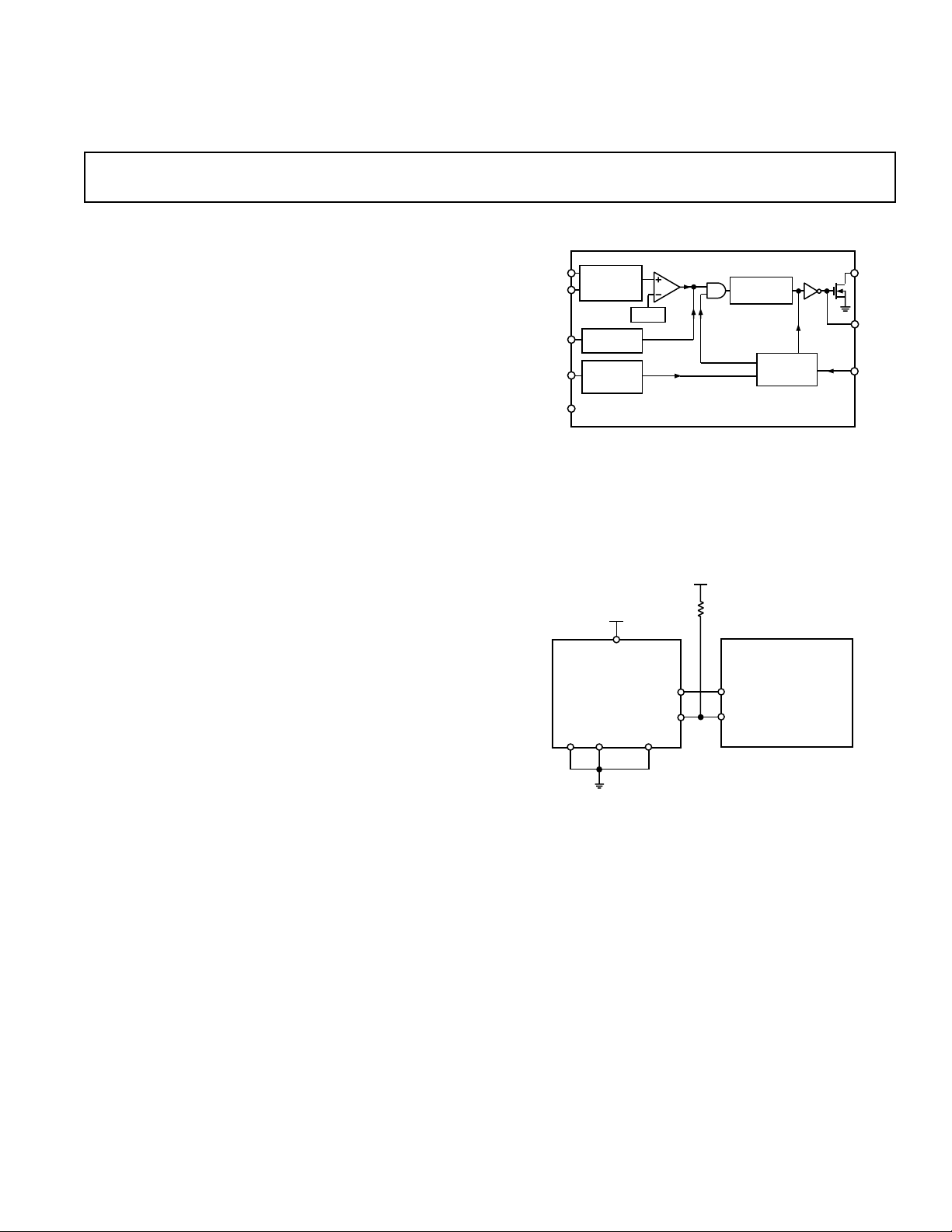
FUNCTIONAL BLOCK DIAGRAM
GENERAL DESCRIPTION
The ADM1232A is a superior, pin-compatible upgrade for the
MAX1232 and the DS1232LP and DS1232. The ADM1232A
can detect strobe pulsewidths as narrow as 20 ns, making it
compatible with high speed microprocessors. The Analog
Devices ADM1232A is a microprocessor monitoring circuit
that can monitor:
1. Microprocessor Supply Voltage.
2. Whether a Microprocessor has locked up.
3. An External Interrupt.
The ADM1232A is available in four different packages:
1. The ADM1232AARM in an 8-lead µSOIC (RM-8).
2. The ADM1232AAN in an 8-lead PDIP (N-8).
3. The ADM1232AARW in a 16-lead wide SOIC (R-16).
4. The ADM1232AARN is an 8-lead narrow SOIC (R-8).
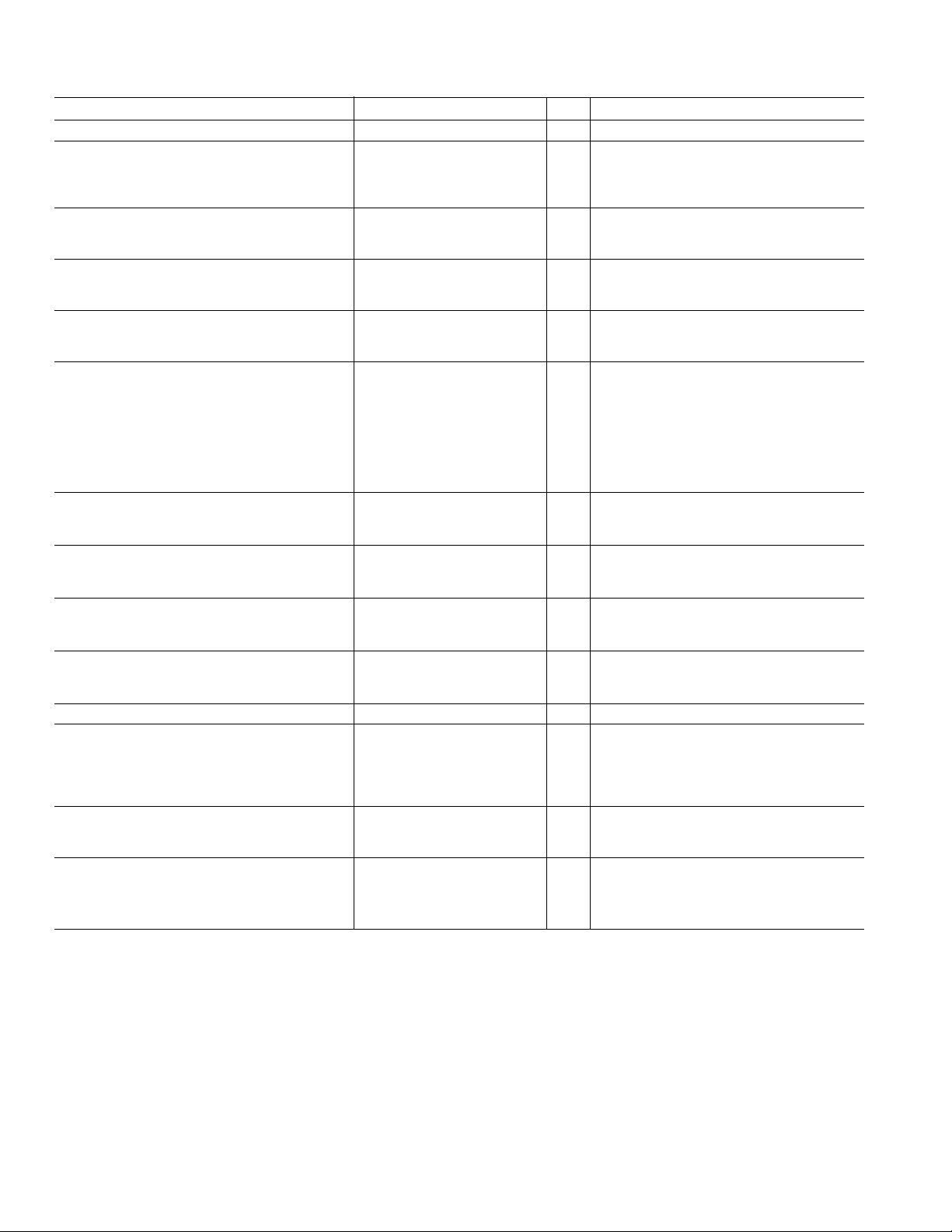
Figure 1. Typical Supply Monitoring Application
REV. 0
Information furnished by Analog Devices is believed to be accurate and
reliable. However, no responsibility is assumed by Analog Devices for its
use, nor for any infringements of patents or other rights of third parties
which may result from its use. No license is granted by implication or
otherwise under any patent or patent rights of Analog Devices.
One Technology Way, P.O. Box 9106, Norwood, MA 02062-9106, U.S.A.
Tel: 781/329-4700 World Wide Web Site: http://www.analog.com
Fax: 781/326-8703 © Analog Devices, Inc., 1999
Page 2
ADM1232A–SPECIFICATIONS
P
arameter Min Typ Max Units Test Conditions/Comments
(VCC = Full Operating Range, TA = T
TEMPERATURE –40 +85 °CT
MIN
= T
A
to T
unless otherwise noted)
MAX
to T
MIN
MAX
POWER SUPPLY
Voltage 4.5 5.0 5.5 V
Current 20 50 µAV
200 500 µAV
, VIH = CMOS Levels
IL
, VIH = TTL Levels
IL
STROBE AND PB RESET INPUTS
Input High Level 2.0 V
+ 0.3 V
CC
Input Low Level –0.3 +0.8 V
INPUT LEAKAGE CURRENT
(STROBE, TOLERANCE) –1.0 +1.0 µA
TD 1.6 µA
OUTPUT CURRENT
RESET 8 10 mA When V
Is at 4.5 V–5.5 V
CC
RESET, RESET –8 –12 mA When VCC Is at 4.5 V–5.5 V
OUTPUT VOLTAGE
RESET/RESET V
– 0.5 V
CC
– 0.1 V While sourcing less than 500 µA, RESET remains
CC
within 0.5 V of V
on power-down until V
CC
CC
drops below 2.0 V. While sinking less than
500 µA, RESET remains within 0.5 V of GND
on power-down until V
drops below 2.0 V.
CC
RESET/RESET High Level 0.4 V
RESET/RESET Low Level 2.4 V
1 V OPERATION
RESET Output Voltage V
– 0.1 V While Sourcing Less than 50 µA
CC
RESET Output Voltage 0.1 V While Sinking Less than 50 µA
TRIP POINT
V
CC
5% 4.5 4.62 4.74 V TOLERANCE = GND
10% 4.25 4.37 4.49 V TOLERANCE = V
CC
CAPACITANCE
Input (STROBE, TOLERANCE) 5 pF T
Output (RESET, RESET)7pFT
= +25°C
A
= +25°C
A
PB RESET
Time 20 ms PB RESET Must Be Held Low for a Minimum
Delay 1 4 20 ms of 20 ms to Guarantee a Reset
RESET ACTIVE TIME 250 610 1000 ms
STROBE
Pulsewidth 20 ns
Timeout Period 62.5 150 250 ms TD = 0 V
250 600 1000 ms TD = Floating
500 1200 2000 ms TD = V
V
CC
Fall Time 10 µ
Rise Time 0 µ
FAIL DETECT TO RESET OUTPUT DELAY
V
CC
S
S
RESET AND RESET Are Logically Correct 50 µs After V
CC
Guaranteed by Design
Guaranteed by Design
Falls Below the Set Tolerance Voltage
CC
(Figure 5)
250 610 1000 ms After VCC Rises Above the Set Tolerance Voltage
Specifications subject to change without notice.
–2–
REV. 0
Page 3

ADM1232A
WARNING!
ESD SENSITIVE DEVICE
ABSOLUTE MAXIMUM RATINGS*
(T
= +25°C unless otherwise noted)
A
VCC . . . . . . . . . . . . . . . . . . . . . . . . . . . . . . . . . . . . . . . . +5.5 V
Logic Inputs . . . . . . . . . . . . . . . . . . . . . –0.3 V to V
+ 0.3 V
CC
Storage Temperature Range . . . . . . . . . . . . –65°C to +150°C
Lead Temperature (Soldering, 10 sec) . . . . . . . . . . . . +300°C
Vapor Phase (60 sec) . . . . . . . . . . . . . . . . . . . . . . . . +215°C
Infrared (15 sec) . . . . . . . . . . . . . . . . . . . . . . . . . . . . +220°C
N-8
Power Dissipation . . . . . . . . . . . . . . . . . . . . . . . . . . 1000 mW
Derate by 13.5 mW/°C above 25°C
Thermal Impedance . . . . . . . . . . . . . . . . . . . . . 100°C/W
θ
JA
R-16
Power Dissipation . . . . . . . . . . . . . . . . . . . . . . . . . . . 900 mW
Derate by 12 mW/°C above 25°C
Thermal Impedance (Still Air) . . . . . . . . . . . . . . 73°C/W
θ
JA
ORDERING GUIDE
Model Range Options*
ADM1232AARM –40°C to +85°C RM-8
ADM1232AAN –40°C to +85°C N-8
ADM1232AARW –40°C to +85°C R-16
ADM1232AARN –40°C to +85°CR-8
*N = Plastic DIP; R = Small Outline; RM = µSOIC.
RM-8
Power Dissipation . . . . . . . . . . . . . . . . . . . . . . . . . . . 900 mW
Derate by 12 mW/°C above 25°C
θ
Thermal Impedance (Still Air) . . . . . . . . . . . . . 206°C/W
JA
R-8
Power Dissipation . . . . . . . . . . . . . . . . . . . . . . . . . . . . 900 µW
Derate by 12 mW/°C above 25°C
Thermal Impedance (Still Air) . . . . . . . . . . . . . 153°C/W
θ
JA
*Stresses above those listed under Absolute Maximum Ratings may cause perma-
nent damage to the device. This is a stress rating only; functional operation of the
device at these or any other conditions above those listed in the operational
sections of this specification is not implied. Exposure to absolute maximum ratings
for extended periods of time may affect device reliability.
Temperature Package
CAUTION
ESD (electrostatic discharge) sensitive device. Electrostatic charges as high as 4000 V readily
accumulate on the human body and test equipment and can discharge without detection.
Although the ADM1232A features proprietary ESD protection circuitry, permanent damage may
occur on devices subjected to high energy electrostatic discharges. Therefore, proper ESD
precautions are recommended to avoid performance degradation or loss of functionality.
REV. 0
–3–
Page 4

ADM1232A
1
2
3
4
8
7
6
5
TOP VIEW
(Not to Scale)
ADM1232A
PB RESET
RESET
STROBE
V
CC
TD
TOLERANCE
GND
RESET
PIN FUNCTION DESCRIPTIONS
Mnemonic Function
PB RESET Push Button Reset Input. This debounced input will ignore pulses of less than 1 ms and is guaranteed to re-
spond to pulses greater than 20 ms.
TD Time Delay Set allows the user to select the maximum amount of time the ADM1232A will allow the STROBE
input to remain inactive (i.e., STROBE is not receiving any high-to-low transitions), without forcing the
ADM1232A to generate a RESET pulse. (See STROBE specifications, Figure 4 and the note on STROBE
timeout selection.)
TOLERANCE Tolerance Input. This input will determine how much the supply voltage will be allowed to decrease (as a per-
centage tolerance) before a RESET is asserted. Connect to V
GND 0 V ground reference for all signals.
RESET Active high logic output. Will be asserted when:
1. V
decreases below the amount specified by the TOLERANCE input or,
CC
2. PB RESET is forced low or,
3. If there are no high-to-low transitions within the limits set by TD at STROBE or,
4. During power-up.
RESET Inverse of RESET, with an open drain output.
STROBE The STROBE input is used to monitor the activity of a microprocessor. If there are no high-to-low transi-
tions within the time specified by TD, a reset will be asserted.
V
CC
Power supply input +5 V.
for 10% and GND for 5%.
CC
NC
PB RESET
NC
TD
NC
TOLERANCE
NC
GND
R-16
1
2
3
ADM1232A
4
TOP VIEW
5
(Not to Scale)
6
7
8
NC = NO CONNECT
16
15
14
13
12
11
10
9
NC
V
CC
NC
STROBE
NC
RESET
NC
RESET
PIN CONFIGURATIONS
RM-8
GND
TD
1
ADM1232A
2
TOP VIEW
(Not to Scale)
3
4
PB RESET
TOLERANCE
8
7
6
5
V
CC
STROBE
RESET
RESET
N-8 and R-8
–4–
REV. 0
Page 5

ADM1232A
V
CC
RESET
+5V
RESET
+4.5V (5% TRIP POINT)
RESET OUTPUT DELAY
WHEN IS V
CC
FALLING
RESET OUTPUT DELAY
WHEN IS VCC RISING
+5V
+4.25V (10% TRIP POINT)
CIRCUIT INFORMATION
PB RESET
The PB RESET input makes it possible to manually reset a system
using either a standard push-button switch or a logic low
input. An internal debounce circuit provides glitch immunity
when used with a switch, reducing the effects of glitches on the
line. The debounce circuit is guaranteed to cause the ADM1232A
to assert a reset if PB RESET is brought low for more than 20 ms
and is guaranteed to ignore low inputs of less than 1 ms.
V
CC
V
CC
ADM1232A
PB RESET
GND
ADM1232
ADM1232
STROBE
TOLERANCE
TOLERANCE
TD
RESET
STROBE
RESET
MICROPROCESSOR
I/O
RESET
Figure 2. Typical Push Button Reset Application
PB RESET TIME
PB RESET
RESET
RESET
PB RESET
DELAY
V
IL
Figure 3.
PB RESET
V
IH
RESET ACTIVE
TIME
STROBE Timeout Selection
TD or time delay set is used to set the Strobe Timeout Period.
The Strobe Timeout Period is defined as being the maximum
time between high-to-low transitions (Figure 4) that STROBE
will accept before a reset will be asserted. The Strobe timeout
settings are listed in Table I.
Table I.
Condition Min Typ Max Units
TD = 0 V 62.5 150 250 ms
TD = Floating 250 600 1000 ms
TD = V
CC
STROBE
500 1200 2000 ms
STROBE
PULSEWIDTH
STROBE TIMEOUT PERIOD
Figure 4.
STROBE
Parameters
Figure 5. Reset Output Delay
TOLERANCE
The TOLERANCE input is used to determine the level VCC can
vary below 5 V without the ADM1232A asserting a reset. Connecting TOLERANCE to ground will select a –5% tolerance
level and will cause the ADM1232A to generate a reset if V
CC
falls below 4.75 V (typical). If TOLERANCE is connected to
a –10% tolerance level is selected and will cause the
V
CC
ADM1232A to generate a reset if V
Check the parameters for the V
falls below 4.5 V (typical).
CC
trip point in the ADM1232A
CC
Specifications for more information.
REV. 0
RESET AND RESET OUTPUTS
While RESET is capable of sourcing and sinking current,
RESET is an open drain MOSFET which sinks current only.
Therefore, it is necessary to pull this output high.
–5–
Page 6

ADM1232A
OUTLINE DIMENSIONS
Dimensions shown in inches and (mm).
0.0118 (0.30)
0.0040 (0.10)
0.122 (3.10)
0.114 (2.90)
0.006 (0.15)
0.002 (0.05)
SEATING
0.4133 (10.50)
0.3977 (10.00)
16 9
PIN 1
0.0500
0.0192 (0.49)
(1.27)
0.0138 (0.35)
BSC
0.122 (3.10)
0.114 (2.90)
8
1
PIN 1
0.0256 (0.65) BSC
0.120 (3.05)
0.112 (2.84)
0.018 (0.46)
0.008 (0.20)
PLANE
16-Lead Wide SOIC
(R-16)
0.2992 (7.60)
0.2914 (7.40)
0.4193 (10.65)
81
0.1043 (2.65)
0.0926 (2.35)
SEATING
PLANE
0.3937 (10.00)
0.0125 (0.32)
0.0091 (0.23)
8-Lead SOIC
(RM-8)
5
0.199 (5.05)
0.187 (4.75)
4
0.043 (1.09)
0.037 (0.94)
0.011 (0.28)
0.003 (0.08)
0.0291 (0.74)
0.0098 (0.25)
0.0500 (1.27)
88
08
0.0157 (0.40)
0.120 (3.05)
0.112 (2.84)
338
278
3 458
0.028 (0.71)
0.016 (0.41)
0.210 (5.33)
MAX
0.160 (4.06)
0.115 (2.93)
0.022 (0.558)
0.014 (0.356)
0.2440 (6.20)
0.2284 (5.80)
0.0098 (0.25)
0.0040 (0.10)
SEATING
0.430 (10.92)
0.348 (8.84)
8
14
PIN 1
0.100
(2.54)
BSC
0.1968 (5.00)
0.1890 (4.80)
85
PIN 1
0.0500
(1.27)
PLANE
BSC
8-Lead PDIP
(N-8)
5
0.280 (7.11)
0.240 (6.10)
0.060 (1.52)
0.015 (0.38)
0.070 (1.77)
0.045 (1.15)
0.130
(3.30)
MIN
SEATING
PLANE
0.325 (8.25)
0.300 (7.62)
8-Lead Narrow SOIC
(R-8)
0.1574 (4.00)
0.1497 (3.80)
41
0.102 (2.59)
0.094 (2.39)
0.0192 (0.49)
0.0138 (0.35)
0.0098 (0.25)
0.0075 (0.19)
0.015 (0.381)
0.008 (0.204)
0.0196 (0.50)
0.0099 (0.25)
88
08
0.0500 (1.27)
0.0160 (0.41)
C3421–8–7/99
0.195 (4.95)
0.115 (2.93)
3 458
–6–
PRINTED IN U.S.A.
REV. 0
 Loading...