

Page 1
© 2005
Preliminary Technical Data
FEATURES
Enables Power Supply Tracking of multiple supplies
Up/Down Tracking limits Supply Differences to ~100mV
Capacitor Adjustable Slew Rate
On Board Charge Pump Fully enhances FET
Emergency Shutdown Feature
In-Built Power Fail Detector Circuitry
Packaged in tiny 8-Lead TSOT Package
APPLICATIONS
Multi-Voltage Supply Rail Tracker
Telecoms and Datacoms Systems
Multi voltage Network Processors
Multivoltage FPGAs, ASICs, DSPs
PC/Server Applications
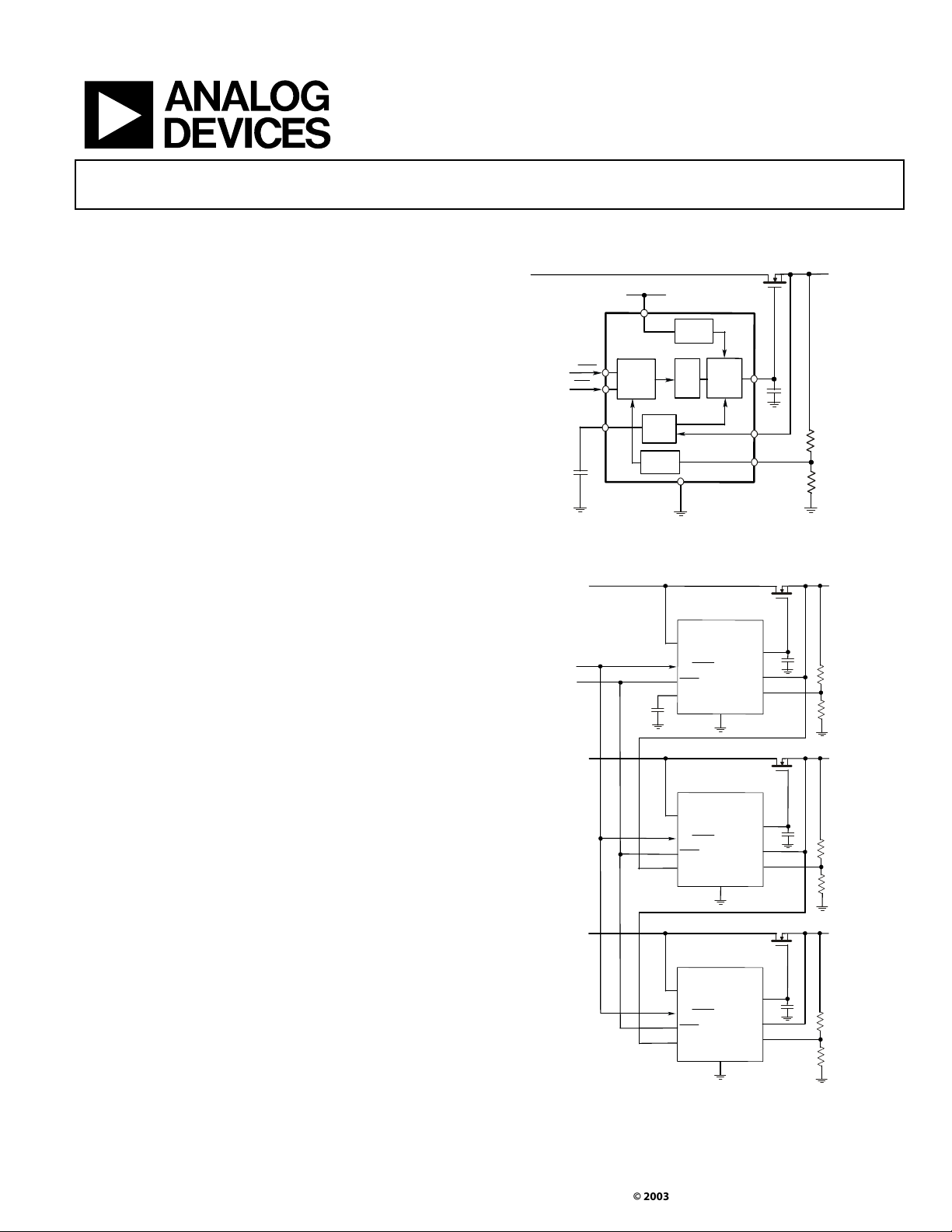
GENERAL DESCRIPTION
The ADM1201 is a cascadable Simple Tracker
ensures that voltage rails track up and ramp within ~100mV of
each other in multi supply systems. Any number of these
devices can be cascaded to form a multi supply tracking
solution. The ADM1201 requires 2.7V to 16.5V on its Vcc pin
to operate. An on-board charge pump generates a high voltage
GATE drive to fully enhance FETs in the power path.
The Slew Rate of the ramp up and ramp down is adjustable via
an external capacitor on the C
pin and can be programmed
SLEW
from 100V/s to 1000V/s. When multiple devices are cascaded
the C
pin of each subsequent device should be tied to the
SLEW
output rail of the previous device to ensure that supply will
track up and down with the previous supply.
TM
device which
Simple Tracker
with Emergency Shutdown
Functional Block Diagram
V
IN
C
SLEW
Applications Diagram
5VIN
POWER ON/OFF
EMERGENCY
SHUTDOWN
3.3VIN
UP/DOWN
STOP
C
SLEW
2.7V - 16V
UP / DOWN
DETECTOR
V
CC
SLEWRATE
CONTROL
POWER FAIL
DETECTOR
GND
CHARGE
PUMP
LOGIC
ADM1201
ADM1201
V
cc
UP/DOWN
STOP
C
SLEW
DRIVER
GND
TM
ADM1201
Q
1
V
FET
GATE
FET
V
OUTFB
PFI
Q
1
GATE
20nF
V
OUT
PFI
Q2
V
R
1
R
2
5VOUT
R
1
R
2
3.3VOUT
OUT
The ADM1201 features an Up/Downb pin for external control
of the Up and Down tracking. A low-to-high transition on the
this input will initiate tracking power up sequence., while a
high-to-low will initiate a tracking down of the supply rails. A
STOPb pin is also available- a high-to-low on this pin will
initiate an emergency fast shutdown of the supply..
Power Fail Detector circuitry is also present. A resistor divider
on the PFI input will dictate what level the ADM1201 registers a
power fail on that supply. When a power fail is detected the
internal Power Fail Comparator will pull the STOPb pin down
which will shut down the output immediately. STOPb pins of
multiple ADM1201 devices may be tied together so that a fault
on any supply rail will cause all devices to go into emergency
shutdown.
The ADM1201 is available in a tiny 8-pin TSOT package.
Rev. PrG
Information furnished by Analog Devices is believed to be accurate and reliable.
However, no responsibility is assumed by Analog Devices for its use, nor for any
infringements of patents or other rights of third parties that may result from its
use. Specifications subject to change without notice. No license is granted by
implication or otherwise under any patent or patent rights of Analog Devices.
Trademarks and registered trademarks are the property of their respective
companies.
ADM1201
V
2.8VIN
cc
UP/DOWN
STOP
C
SLEW
GND
GATE
V
OUT
PFI
20nF
Q3
ADM1201
V
cc
UP/DOWN
STOP
C
SLEW
One Technology Way, P.O. Box 9106, Norwood, MA 02062-9106, U.S.A.
Tel: 781.329.4700
www.analog.com
GND
GATE
V
OUT
PFI
20nF
Fax: 781.326.8703© 2003 Analog Devices, Inc. All rights reserved.
R
3
R
4
2.8VOUT
R
5
R
6
Page 2

Preliminary Technical Data
ADM1201—SPECIFICATIONS
Table 1. V
Parameter Min Typ Max Units Conditions
VCC Pin
Operating Voltage Range Vcc 2.7 16.5 V
Undervoltage Lockout, V
UVLO Hysteresis 25 mV
Switched Voltage Range 0.65 16.5
Quiesent Current 0.65 1.0
Up/Downb Pin
Input Threshold 0.58 0.6 0.62
Input Threshold Hysteresis 60 mV
Input Current
Stopb Pin
Input Threshold 0.58 0.6 0.62
Input Threshold Hysteresis 60 mV
Internal Pull Up -5
Output Low Voltage 0.4 V Note 1, Iload = 300uA
Power Fail Detector, PFI Pin
PFI Detector Threshold
PFI Detector Hysterisis
PFI Input Current
C
Pin
SLEW
Slew up Current
Slew down Current
Tracking Gain 1 V/V V
Minimum Tracking Voltage 0.1 V
Maximum Tracking voltage Vcc – 0.3 V
Slew Rate
V
Pin
OUTFB
Input Current
Voltage Range 0 Vcc V
GATE Pin
Gate Pullup Current 12
Gate Pulldown Current 12
Gate Pulldown Current 2
GATE Voltage, V
6 8 12 V V
5 6.5 10 V V
NOTES:
1
Activated when voltage on PFI pin exceeds threshold
= Full Operating Range, TA = -40°C to +85°C, unless otherwise noted.
CC
2.4 2.525 2.65 V Vcc Rising
UVLO
5 6.5 10 V V
GATE
-100 100 nA
0.58 0.6 0.62 V
20 mV
-100 100 nA
-10
10
100 1000 V/s
-10 10
V
mA
V
V
µA
µA
µA
µA
µA
µA
mA
Rising
Rising
SLEW/VOUTFB
Vslew – Vout > 100mV
Vout – Vslew > 100mV
ADM1202-2 only –vgate = 3.0V
– VCC; VCC = 2.7V
GATE
– VCC; VCC = 5.0V
GATE
– VCC; VCC = 16.5V
GATE
Rev. PrG | Page 2 of 6
Page 3

Preliminary Technical Data ADM1201
ENABLING A SINGLE SUPPLY
The ADM1201 requires a supply voltage of 2.7V to 16.5V on its
Vcc pin for operation. The device may be powered from the
input supply rail that is being switched or from an auxiliary
supply.
An internal charge pump ensures that the ADM1201 is capable
of fully enhancing an external FET via the GATE pin. An
external capacitor may be required on the GATE node for
stability.
Power up can be externally initiated by driving the
UP/DOWNb logic pin high. A low on this pin will initiate a
power down. The V
pin monitors the output voltage.
OUTFB
A single ADM1201 device may be used where a single supply
rail is required to switch on at a controlled slew rate (see Figure
1). The value of the slew rate capacitor, C
, will dictate the
SLEW
slew rate of the GATE voltage at startup. An internal current
source charges C
and the GATE voltage is ramped at the
SLEW
same rate.
Q
3.3VIN
1
3.3VOUT
ADM1201
V
POWER ON/OFF
EMERGENCY
SHUTDOWN
cc
UP/DOWN
STOP
C
SLEW
GND
GATE
V
OUTFB
PFI
20nF
R
1
R
2
Figure 1. ADM1201 Switching on a Single Supply
MULTI-SUPPLY TRACKING
The primary function of the ADM1201 is to provide a voltage
tracking solution for multiple supply rails. The implementation
in Figure 2 will provide this function. Each voltage rail has its
own ADM1201 device driving a FET.
Q
5VIN
1
5VOUT
ADM1201
V
POWER ON/OFF
EMERGENCY
SHUTDOWN
3.3VIN
cc
UP/DOWN
STOP
C
SLEW
GND
V
OUTFB
GATE
PFI
20nF
R
1
R
2
Q2
3.3VOUT
ADM1201
V
2.8VIN
cc
UP/DOWN
STOP
C
SLEW
GND
V
OUTFB
GATE
PFI
20nF
R
3
R
4
Q3
2.8VOUT
ADM1201
V
cc
UP/DOWN
STOP
C
SLEW
GND
GATE
V
OUTFB
20nF
PFI
R
5
R
6
Figure 2. ADM1201 Solution for Tracking 3 Supplies
A low-to-high transition on the UP/DOWNb pin will initiate
turn-on of the supplies. The ADM1201 will begin to source
current into the C
capacitor. The voltages on all GATE pins
SLEW
will begin to rise, or “track” up, at the same rate, as set by the
value of C
the C
SLEW
. All supply voltages will remain within 100mV of
SLEW
voltage until they level off at their full potentials.
A high-to-low on the UP/DOWNb pin of the ADM1201 will
initiate a tracking down of the supply rails, while a high-to-low
on the STOPb pin of the ADM1201 will initiate an emergency
fast shutdown of all supply rails simultaneously.
The UP/DOWNb pins of all devices can be driven by a single
logic input which will initiate a system power-up going high or
power-down going low.
The C
pins of all subsequent devices should be tied to the
SLEW
supply that the controlled needs to be tracked with. If multiple
parts are configured as in Figure 2 then the C
capacitor on
SLEW
the first ADM1201 will set the slew rates for all devices.
Rev. PrG | Page 3 of 6
Figure 3 show power-up and power-down waveforms for the
ADM1201.
Page 4

ADM1201 Preliminary Technical Data
A
UP/DOWN
STOP
OUTPUT
VOLTAGES
3.3V
2.5V
1.5V
3.3V
2.5V
1.5V
Figure 3. ADM1201 Power-Up and Power-Down Waveforms
(Condition 1) and a voltage is detected on the output
(Condition 2) when Power Fail Circuitry is enabled. The output
of the PFI block is internally connected to the STOPb pin. So if
a power fail condition on the output is detected after startup,
the STOPb will be pulled low internally, initiating an emergency
shutdown of the supply rail. When multiple ADM1201 devices
are cascades all STOPb pins may be wired together so that a
power fail on any output after start-up will initiate a systemwide emergency shutdown of all supply rails.
POWER FAIL DETECTOR
Figure 4 below shows the internal circuitry that enables the
Power Fail Detector. When the ADM1201 powers up initially
the Power Fail Detector is disabled. Two conditions must be
met before the Power Fail Detector is enabled:
1. The voltage on the slew rate capacitor, C
at or above V
. This ensures that the PFI Detector is
CC
, must be
SLEW
only enabled once the supply rail has been turned on.
2. The voltage on the PFI pin must be greater than 0.4V.
This ensures that some voltage greater than zero is
present on the output (and that a fault is not pulling
the output down).
When the GATE is ramped up and the output is turned on
DM1201 Truth Table
UP/DOWNb STOPb GATE
(Input) ( I/O) (Output)
00OFF
01OFF
10*OFF
11ON
* A high-to-low on STOPb will initiate an emergency
(fast) gate shutdown of all ADM1201 devices with STO Pb
pins connected.
Figure 5. ADM1201 Power-Up and Power-Down Truth Table
Absolute Maximum Ratings
Table 2. ADM1201 Absolute Maximum Ratings
Parameter
VIN Pin 20V
PFI Pin 20V
Logic Pins Up/Downb, Stopb 20V
C
Pin 20V
SLEW
Gate Pin Vcc +11V
V
Pin 20V
OUT
Power Dissipation TBD
Storage Temperature –65°C to +125°C
Operating Temperature Range –40°C to +85°C
Lead Temperature Range
(Soldering 10 sec)
Junction Temperature 150°C
Rating
300°C
Rev. PrG | Page 4 of 6
Page 5

Preliminary Technical Data ADM1201
PIN CONFIGURATION
V
UP / DO WN
1
ADM1201AUJ
8
CC
GND
STOP
V
OUTFB
2
TOP VIEW
(Not to Scale)
3
4
7
6
5
PFI
GATE
C
SLEW
PIN FUNCTIONAL DESCRIPTIONS
Pin No. Name Description
1 UP/DOWNb Logic Pin. Drive high to initiate Power Up; Drive low to initiate Power Down.
2 GND Chip Ground Pin
3 STOPb Logic Pin. Drive low trigger an emergency shutdown of all supply.
4 VOUTFB Monitors the Source of the external FET
5 CSLEW
6 GATE Drives the GATE node of the external FET
7 PFI
8 VCC Chip Power Supply, 2.7V to 16.5V.
Connect to an external capacitor to control the slew rate of the of the GATE at turn on
(and turn-off for ADM1201-1).
Power Fail Detector Input Pin. A power fail fault is registered at a voltage of 0.6V on this
pin. An external resistor divider sets the output voltage that trips a power fail fault.
Rev. PrG | Page 5 of 6
Page 6

ADM1201 Preliminary Technical Data
2005
PR05129-0-2/05(PrG)
OUTLINE DIMENSIONS
Figure XX. 8-Lead TSOT Package (UJ-8)—Dimensions shown in millimeters
ESD CAUTION
ESD (electrostatic discharge) sensitive device. Electrostatic charges as high as 4000 V readily accumulate on the
human body and test equipment and can discharge without detection. Although this product features
proprietary ESD protection circuitry, permanent damage may occur on devices subjected to high energy
electrostatic discharges. Therefore, proper ESD precautions are recommended to avoid performance
degradation or loss of functionality.
Table 3. Ordering Guide
Part Number Temperature Package Package Description Package Outline
ADM1201AUJ –40°C to +85°C TSOT UJ-8
003 Analog Devices, Inc. All rights reserved. Trademarks and
registered trademarks are the property of their respective companies.
Printed in the U.S.A.
Rev. PrG | Page 6 of 6
 Loading...