

Page 1
© 2005
2.7V to 16.5V Hot Swap Controller
Preliminary Technical Data
FEATURES
Allows Safe Board Insertion and Removal from a Live
Backplane
Controls Supply Voltages from 2.7 V to 16.5V
Adjustable Analog Current Limit with Circuit Breaker
Fast Response Limits Peak Fault Current
Automatic Retry or Latch-Off On Current Fault
Adjustable Voltage Slew Rate Control
Charge Pumped Gate Drive for External N-FET Switch
TIMER pin allows control over timing functions
Undervoltage Lockout
8-pin TSOT Package
APPLICATIONS
Hot Swap Board Insertion – Line Cards, Raid systems
Electronic Circuit Breaker
Industrial High Side Switch/Circuit Breaker
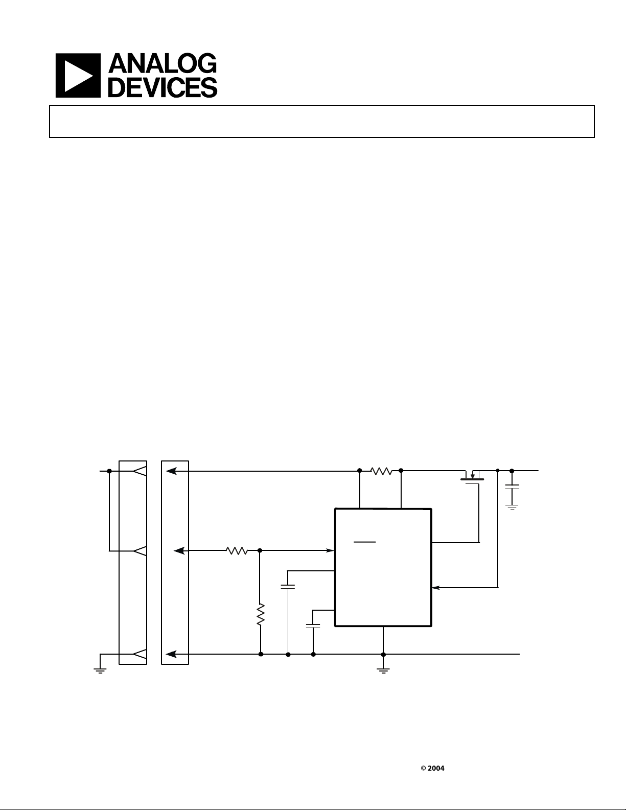
APPLICATIONS DIAGRAM
VIN=5V
LONG
with Tracking or Slew Rate Control
ADM1173
GENERAL DESCRIPTION
The ADM1173 is a Hot Swap controller that allows a board to
be safely inserted and removed from a live backplane.
An internal charge pumped driver controls the GATE of an
external high side N-channel FET for a supply voltage ranging
from 2.7V to 16.5V. The ADM1173 provides the initial timing
cycle and allows the GATE to be ramped up at an adjustable
rate. The Slew rate of the Output is controlled a capacitor or
supply on the SLEW pin.
The ADM1173 features a fast current limit loop providing
active current limiting together with a circuit breaker timer.
The signal at the ON pin turns the part on and off and is also
used for the reset function.
A capacitor connected to the TIMER pin gives the user control
over the duty cycle of the PWM retry ratio during current fault.
This part is available in two options: the ADM1173-1 will
automatic retry for over-current fault and the ADM1173-2 will
latch-off for an over-current fault.
The ADM1173 is packaged in an 8-lead TSOT package.
R
SENSE
Q
1
V
C
OUT
LOAD
=5V
R
SHORT
GND
Rev.PrE
Information furnished by Analog Devices is believed to be accurate and reliable.
However, no responsibility is assumed by Analog Devices for its use, nor for any
infringements of patents or other rights of third parties that may result from its use.
Specifications subject to change without notice. No license is granted by implication
or otherwise under any patent or patent rights of Analog Devices. Trademarks and
registered trademarks are the property of their respective companies.
LONG
ON1
R
C
ON2
SLEW
cc
SENSE-
GATE
V
ON / CLR
ADM1173
SLEW
VOUT
TIMER
C
TIMER
One Technology Way, P.O. Box 9106, Norwood, MA 02062-9106, U.S.A.
Tel: 781.329.4700
Fax: 781.326.8703 © 2004 Analog Devices, Inc. All rights reserved.
GND
GND
www.analog.com
Page 2

Preliminary Technical Data ADM1173
SPECIFICATIONS
Table 1. V
Parameter Min Typ Max Units Conditions
VCC Pin
Operating Voltage Range, VCC 2.7 16.5 V
Supply Current, Icc 0.65 1.0
Undervoltage Lockout, V
Undervoltage Lockout Hysteresis, V
ON Pin
ON Pin Input Current, I
On Pin Threshold, VON 1.26 1.3 1.34
ON Pin Threshold Hysteresis, V
RS- Pin
Hot Swap Voltage 2.7 16.5
RS- Pin Input Current, I
Circuit Breaker Limit Voltage, VCB 34 47 60
44 47 53
Over Current Limit Voltage, VOC 40 53 66
50 53 59
GATE Pin
GATE Drive Voltage, V
GATE Drive Voltage, V
GATE Drive Voltage, V
Gate Pullup Current
Gate Pulldown Current
Gate Pulldown Current
TIMER Pin
TIMER Pin Pull-Up Current, I
-48 -60 -72
TIMER Pin Pull-Down Current, I
100
TIMER Pin Threshold High, V
TIMER Pin Threshold Low, V
C
Pin
SLEW
Slew up Current
Slew down Current
Tracking Gain 1 V/V V
Tracking Accuracy -100 100 mV
Minimum Tracking Voltage 0.1 V
Maximum Tracking voltage Vcc – 0.1 V
Slew Rate
V
Pin
OUTFB
Input Current
Voltage Range 0 Vcc V
= 2.7V to 16V, TA = -40°C to +85°C, Typical Values at TA = 25°C unless otherwise noted.
CC
mA
2.4 2.525 2.65 V VCC Rising
UVLO
25
INON
UVLOHYS
-100 0 100
mV
nA
V
80
ONHYST
mV
V
INSENSE
TBD -200 TBD
10 20 30
µA
µA
mV
mV
mV
mV
GATE
6 8 12 V V
GATE
5 6.5 10 V V
GATE
5 6.5 10 V V
10 12 14 uA V
2 mA V
25 mA V
-4 -5 -6
TIMERUP
µA
µA
TIMERDN
2 2.5
µA
µA
1.235 1.3 1.365
TIMERH
0.18 0.2 0.22
TIMERL
V
V
-10
10
100 1000 V/s
µA
µA
-100 100
µA
ON rising
V
= VCC, V
SENSE
V
= VCC, V
SENSE
VCB = (V
VCB = (V
V
HOTSWAP
V
HOTSWAP
GATE
GATE
GATE
GATE
GATE
GATE
– V
CC
– V
CC
= 0.6 V, Note
> 2.2 V
– VCC, VCC = 2.7V
– VCC, VCC = 5V
– VCC, VCC = 16.5V
= 0V
= 3V, Vcc > UVLO
= 3V, Vcc < UVLO
Initial Cycle, V
HOTSWAP
HOTSWAP
SENSE
SENSE
TIMER
) ,V
) ,V
= 0.6 V, Note
> 2.2 V
HOTSWAP
HOTSWAP
= 1V
During Current Fault, V
After Current Fault, V
Normal Operation, V
TIMER
TIMER rising
TIMER falling
SLEW/VOUTFB
TIMER
TIMER
= 1V
= 1V
= 0.6 V
> 2.2 V
= 1V
Rev. PrE | Page 2 of 8
Page 3
Preliminary Technical Data ADM1173
Absolute Maximum Ratings
Parameter
VCC Pin 20V
RS+, RS- Pins -0.3V to 20V
TIMER Pin -0.3V to (VCC + 0.3V)
Slew Pin -0.3 to 20V
ON Pin -0.3V to 20V
GATE Pin VCC + 11V
Power Dissipation TBD
Storage Temperature –65°C to +125°C
Operating Temperature Range –40°C to +85°C
Lead Temperature Range (10 sec) 300°C
Junction Temperature 150°C
Rating
Rev. PrE | Page 3 of 8
Page 4

Preliminary Technical Data ADM1173
shunts any potential static charge on the backplane and reduces
HOT CIRCUIT INSERTION
When circuit boards are inserted into live backplanes, the
supply bypass capacitors can draw large transient currents
from the backplane power bus as they charge. Such transient
currents can cause permanent damage to connector pins,
glitches on the system supply or reset other boards in the
system.
The ADM1173 is designed to turn a printed circuit board’s
supply voltage ON and OFF in a controlled manner, allowing
the circuit board to be safely inserted into or removed from a
live backplane. The ADM1173 can reside either on the
backplane or on the daughter board for hot circuit insertion
applications.
OVERVIEW
The ADM1173 is designed to operate over a range of supplies
from 2.7V to 16.5V. Upon insertion, an undervoltage lockout
circuit determines if sufficient supply voltage is present. When
the ON pin goes high an initial timing cycle assures that the
board is fully seated in the backplane before the FET is turned
on. A single timer capacitor sets the periods for all of the timer
functions. After the initial timing cycle the ADM1173 can
either start up in current limit or with a lower load current.
Once the external FET is fully enhanced and the supply has
ramped up, the ADM1173 monitors the load current through
an external sense resistor. Overcurrent faults are actively
limited to 47mV/R
limit. The ADM1173-1 will automatically retry after a current
limit fault while the ADM1173-2 latches off. The ADM1173-1
timer function limits the retry duty cycle to 3.8% for FET
cooling.
for a specified circuit breaker timer
SENSE
UNDERVOLTAGE LOCKOUT
An internal undervoltage lockout (UVLO) circuit resets the
ADM1173 if the V
The UVLO has a low-to-high threshold of 2.525V, a 25mV
hysteresis. Above 2.525V supply voltage, the ADM1173 will
start if the ON pin conditions are met.
supply is too low for normal operation.
CC
ON FUNCTION
The ON pin is the input to a comparator which has a low-tohigh threshold of 1.3V, an 80mV hysteresis and a high-to-
low glitch filter of 30µs. A low input on the ON pin resets
the ADM1173 TIMER status and turns off the external FET by
pulling the GATE pin to ground. A low-to-high transition on
the ON pin starts an initial cycle followed by a start-up cycle.
The output will then start to rise at a rate determined by the
slew rate of the SLEW pin. A 10k pull-up resistor connecting
the ON pin to the supply is recommended. The 10k resistor
the overvoltage stress at the ON pin during live insertion.
Alternatively, an external resistor divider at the ON pin can be
used to program an undervoltage lockout value higher than the
internal UVLO circuit. An RC filter can be added at the ON pin
to increase the delay time at card insertion if the internal glitch
filter delay is insufficient.
GATE FUNCTION
During hot insertion of the PCB, an abrupt application of
supply voltage charges the external FET drain/gate capacitance.
This can cause an unwanted gate voltage spike. An internal
circuit holds GATE low before the internal circuitry wakes up.
This reduces the FET current surges substantially at insertion.
The GATE pin is held low in reset mode and during the initial
timing cycle. In the start-up cycle the GATE pin is pulled up by
a 12µA current source. During an over-current fault condition,
the error amplifier servos the GATE pin to maintain a constant
current to the load until the circuit breaker trips. When the
circuit breaker trips, the GATE pin shuts down abruptly.
SLEW RATE CONTROL
The slew rate of a rising or falling supply can be controlled by
an external capacitor on the SLEW pin. Alternatively, this pin
can be overdriven with a supply which will result in the output
following this supply. This enables the ADM1173 to behave as a
voltage tracker.
CURRENT LIMIT CIRCUIT BREAKER FUNCTION
The ADM1173 features a current limiting circuit breaker.
When there is a sudden load current surge, such as a low
impedance fault, the bus supply voltage can drop significantly
to a point where the power to an adjacent card is
affected, causing system malfunctions. The ADM1173 fast
response current sense amplifier instantly limits current by
reducing the external FET GATE pin voltage. This
minimizes the bus supply voltage drop and permits power
budgeting and fault isolation without affecting neighboring
cards. A compensation circuit should be connected to
the GATE pin for current limit loop stability.
Rev. PrE | Page 4 of 8
Page 5

Preliminary Technical Data ADM1173
M
ODE
pulls down the TIMER pin until it reaches 0.2V at time point 4.
CALCULATING CURRENT LIMIT
The nominal fault current limit is determined by a sense
resistor connected between V
given by the equation below:
I
LIMIT(NOM)
= V
CB(NOM)
/ R
SENSE
The minimum load current is given by Equation 2:
I
LIMIT(MIN)
= V
CB(MIN)
/ R
SENSE(MAX)
The maximum load current is given by Equation 3:
and the SENSE pin as
CC
(1)
(2)
The initial cycle delay (time point 2 to time point 4) is related to
by equation:
C
TIMER
t
INITIAL
~= 272.9 x C
ms/uF (4)
TIMER
When the initial cycle terminates, a start-up cycle is activated
and the GATE pin ramps high. The TIMER pin continues to be
pulled down towards ground.
I
LIMIT(MAX)
= V
CB(MAX)
/ R
SENSE(MIN)
(3)
Note: The power rating of the sense resistor should be rated at
the fault current level.
For proper operation, the minimum current limit must exceed
the circuit maximum operating load current with margin. The
sense resistor power rating must exceed V
/R
SENSE(MIN).
CB(MAX
)2
TIMER FUNCTION
The TIMER pin handles several key functions with an external
capacitor, C
COMP1 (0.2V) and COMP2 (1.3V). The four timing current
sources are:
• 5µA pull-up
• 60µA pull-up
• 2µA pull-down
• 100µA pull-down
The 100µA is a non-ideal current source approximating a 7k
resistor below 0.4V.
. There are two comparator thresholds:
TIMER
V
TIMER
V
GATE
V
V
V
ON
OUT
IN
RES ET
INITIAL
CYCL E
START-UP
CYCLE
NORM A L
CYCLE
Figure 1: Normal Start-up
INITIAL TIMING CYCLE
When the card is being inserted into the bus connector, the
long pins mate first which brings up the supply VIN at time
point 1 of Figure 1. The ADM1173 is in reset mode as the ON
pin is low. GATE is pulled low and the TIMER pin is pulled low
with a 100µA source. At time point 2, the short pin makes
contact and ON is pulled high. At this instant, a start-up check
requires that the supply voltage be above UVLO, the ON pin
beabove1.3Vand the TIMER pin voltage be less than 0.2V.
When these three conditions are fulfilled, the initial cycle
begins and the TIMER pin is pulled high with 5µA. At time
point 3, the TIMER reaches the COMP2 threshold and the first
portion of the initial cycle ends. The 100µA current source then
Rev. PrE | Page 5 of 8
Page 6

Preliminary Technical Data ADM1173
KELVIN SENSE RESISTOR CONNECTION
V
V
ON
V
TIMER
V
GATE
V
OUT
I
RSENSE
IN
When using a low-value sense resistor for high current
measurement the problem of parasitic series resistance can
arise. The lead resistance can be a substantial fraction of the
5µA
100µA
60µA
2µA
100µA
rated resistance making the total resistance a function of lead
length. This problem can be avoided by using a Kelvin sense
connection. This type of connection separates the current path
through the resistor and the voltage drop across the resistor.
Figure 18 below shows the correct way to connect the sense
pins of the ADM1173.
CURRENT
Current Flow to
FLOW TO -48V
Load
BACKPLANE
RESET
MODE
INITIAL
CYCLE
START-UP
CYCLE
V
TH
NORMAL
CYCLE
resistor between the VCC and RS-
SENSE RESISTOR
CURRENT
Current Flow
FLOWFROM
LOAD
from source
KELVIN SENSETRACES
Figure 2: Current Limiting at Start-up
SENSE V
EE
VCC RS-
ADM107 3
Figure 2: Current Sense Kelvin connection
Rev. PrE | Page 6 of 8
Page 7

Preliminary Technical Data ADM1173
PIN CONFIGURATIONS
TIMER
1
V
8
CC
TIMER
ADM1173-1AUJ
GND
ON
VOUTFB VOUTFB
2
3
4
TOP VIEW
(Not to Scale)
7
6
5
RS-
SLEW
GATE
ON-CLR
PIN FUNCTIONAL DESCRIPTIONS
Pin No. Name Description
1 TIMER
2 GND Chip Ground Pin
3 UP/STOP
ON (ON-CLR)
4 VOUTFB Monitors the Source of the external FET
Timer Input Pin. An external capacitor C
21.7ms/µF circuit breaker delay. The GATE pin turns off whenever the TIMER pin is pulled
beyond the upper threshold, such as for overvoltage detection with an external zener.
Input Pin. The ON pin comparator has a low-to-high threshold of 1.3V with 80mV
hysteresis and a glitch filter. When the ON pin is low, the ADM1173 is reset. When the
ON pin goes high, the GATE turns on after the initial timing cycle. On the ADM1173-2, a
rising edge on this pin has the added function of clearing a fault and restarting the
device
V
1
8
CC
ADM1173-2AUJ
2
3
TOP VIEW
(Not to Scale)
4
sets a 272.9ms/µF initial timing delay and a
TIMER
7
6
5
RS-GND
SLEW
GATE
5 GATE
6 SLEW
7 R S-
8 VCC
GATE Output Pin. This pin is the high side gate drive of an external N-channel FET. An
internal charge pump provides a 12µA pull-up current with Zener clamps to RS+ and
ground. In overload, the error amplifier (EA) controls the external FET to maintain a
constant load current.
Connect to an external capacitor to control the slew rate of the of the GATE at turn on
and turn-off.
Current Limit Sense Input Pin. A sense resistor between the Vcc and RS- pins sets the
analog current limit. In overload, the EA controls the external FET gate to maintain the
SENSE voltage at 50mV. When the EA is maintaining current limit, the TIMER circuit
breaker mode is activated. The current limit loop/circuit breaker mode can be disabled
by connecting the Vcc pin and RS- pin together.
Positive Supply Input Pin. The operating supply voltage range is between 2.7V to 16.5V.
An undervoltage lockout (UVLO) circuit with a glitch filter resets the ADM1173 when a
low supply voltage is detected.
Rev. PrE | Page 7 of 8
Page 8

ADM1173
Preliminary Technical Data
2005
PR05127-0-2/05(PrE)
OUTLINE DIMENSIONS
Figure 3. 8-Lead TSOT Package (UJ-8)—Dimensions shown in millimeters
ESD CAUTION
ESD (electrostatic discharge) sensitive device. Electrostatic charges as high as 4000 V readily accumulate on the
human body and test equipment and can discharge without detection. Although this product features
proprietary ESD protection circuitry, permanent damage may occur on devices subjected to high energy
electrostatic discharges. Therefore, proper ESD precautions are recommended to avoid performance
degradation or loss of functionality.
Table 2. Ordering Guide
Part Number Version Temperature Package Package Description Package Outline
ADM1173-1AUJ Automatic Retry Version –40°C to +85°C TSOT UJ-8
ADM1173-2AUJ Latched Off Version –40°C to +85°C TSOT UJ-8
2004 Analog Devices, Inc. All rights reserved. Trademarks and
registered trademarks are the property of their respective companies.
Printed in the U.S.A.
 Loading...