

Page 1
2.7 V to 16.5 V Hot Swap Controller
V
www.BDTIC.com/ADI
with Power-Fail Comparator
FEATURES GENERAL DESCRIPTION
Controls supply rails from 2.7 V to 16.5 V
Allows protected board removal and insertion to a live
backplane
External sense resistor provides adjustable analog current
limit with circuit breaker
Peak fault current limited with fast response
Charge pumped gate drive for external N-FET switch
Power-fail comparator
Automatic retry or latch-off during current fault
Undervoltage lockout
8-lead, TSOT package
APPLICATIONS
Hot swap board insertion: line cards, raid systems
Industrial high-side switches/circuit breakers
Electronic circuit breakers
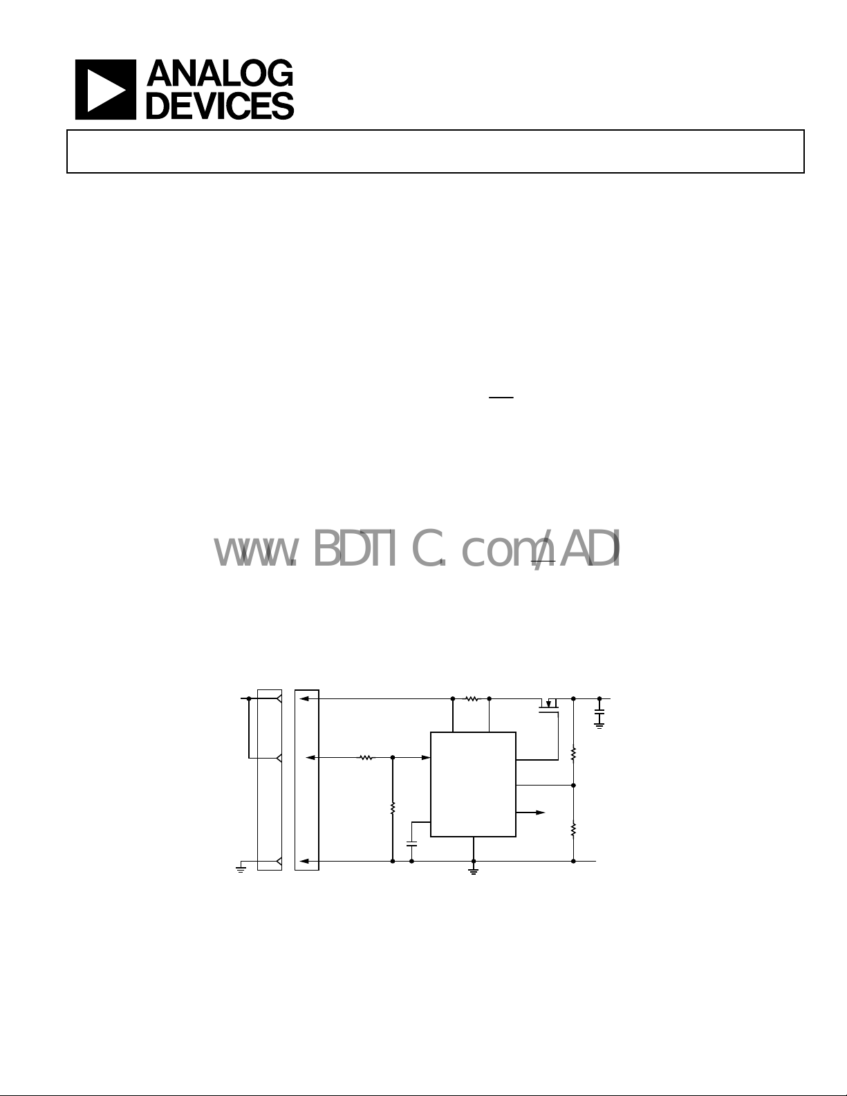
The ADM1172 is a hot swap controller that safely enables a
printed circuit board to be removed and inserted to a live
backplane. This is achieved using an external N-channel power
MOSFET with a current control loop that monitors the load
current through a sense resistor. An internal charge pump is
used to enhance the gate of the N-channel FET. When an overcurrent condition is detected, the gate voltage of the FET is
reduced to limit the current flowing through the sense resistor.
During an overcurrent condition, the TIMER pin capacitor
determines the amount of time the FET remains at a current
limiting mode of operation until it is shut down. The ON
CLR
(ON-
) pin is the enable input for the device and can be
used to monitor the input supply voltage. The ADM1172
operates with a supply voltage ranging from 2.7 V to 16.5 V.
The ADM1172 also features a power-fail comparator. The
voltage on the PFI pin is compared with an internal 0.6 V
reference, and the output of this comparator is presented on
the PFO pin. This device is available in two options: the
ADM1172-1 with automatic retry for overcurrent fault and the
ADM1172-2 with latch-off for an overcurrent fault. Toggling
the ON (ON-
CLR
) pin resets a latched fault. The ADM1172 is
packaged in an 8-lead TSOT.
ADM1172
FUNCTIONAL BLOCK DIAGRAM
= 5V V
IN
GND GND
Rev. 0
Information furnished by Analog Devices is believed to be accurate and reliable. However, no
responsibility is assumed by Anal og Devices for its use, nor for any infringements of patents or ot her
rights of third parties that may result from its use. Specifications subject to change without notice. No
license is granted by implication or otherwise under any patent or patent rights of Analog Devices.
Trademarks and registered trademarks are the property of their respective owners.
LONG
SHORT
LONG
R
ON1
R
ON2
R
SENSE
SENSE
V
CC
ON
ADM1172-1
TIMER
C
TIMER
Figure 1.
GATE
PFI
PFO
GND
One Technology Way, P.O. Box 9106, Norwood, MA 02062-9106, U.S.A.
Tel: 781.329.4700 www.analog.com
Fax: 781.461.3113 ©2006 Analog Devices, Inc. All rights reserved.
Q
1
R
PR1
R
PR2
C
OUT
LOAD
= 5V
05126-001
Page 2

ADM1172
www.BDTIC.com/ADI
TABLE OF CONTENTS
Features.............................................................................................. 1
UVLO........................................................................................... 12
Applications....................................................................................... 1
General Description ......................................................................... 1
Functional Block Diagram .............................................................. 1
Revision History ............................................................................... 2
Specifications..................................................................................... 3
Absolute Maximum Ratings............................................................ 4
Thermal Characteristics .............................................................. 4
ESD Caution.................................................................................. 4
Pin Configurations and Function Descriptions ........................... 5
Typical Performance Characteristics ............................................. 6
Theory of Operation ...................................................................... 12
Overview...................................................................................... 12
REVISION HISTORY
7/06—Revision 0: Initial Version
ON (ON-
GATE ........................................................................................... 12
Current Limit Function............................................................. 12
Calculating the Current Limit.................................................. 12
Circuit Breaker Function........................................................... 12
Timer Function........................................................................... 13
Power-Up Timing Cycle............................................................ 13
Circuit Breaker Timing Cycle................................................... 13
Automatic Retry or Latched Off............................................... 14
Power-Fail Comparator ............................................................. 14
Outline Dimensions....................................................................... 15
Ordering Guide .......................................................................... 15
CLR
) Pin..................................................................... 12
Rev. 0 | Page 2 of 16
Page 3
ADM1172
www.BDTIC.com/ADI
SPECIFICATIONS
VCC = 2.7 V to 16.5 V, TA = −40°C to +85°C, typical values at TA = 25°C, unless otherwise noted.
Table 1.
Parameter Symbol Min Typ Max Unit Conditions
VCC PIN
Operating Voltage Range VCC 2.7 16.5 V
Supply Current ICC 0.65 0.8 mA
Undervoltage Lockout V
Undervoltage Lockout Hysteresis V
ON (ON-CLR) PIN
Input Current
Threshold VON 1.22 1.3 1.38 V ON rising
Threshold Hysteresis V
SENSE PIN
Hot Swap Operating Range 2.7 16.5 V
Input Current
Circuit Breaker Limit Voltage VCB 44 50 56 mV VCB = (VCC – V
GATE PIN
Drive Voltage V
6.0 8 12 V V
8.75 10 12 V V
7.5 9 12 V V
5.56 8 12 V V
Pull-Up Current −6.5 −12 −14.5 A V
Pull-Down Current 4 mA
Pull-Down Current
TIMER PIN
Pull-Up Current I
−25 −60 −100 µA During current fault, V
Pull-Down Current I
100 µA Normal operation, V
Threshold High V
Threshold Low V
PFI PIN
Threshold Rising 0.58 0.6 0.62 V
Threshold Hysteresis 10 mV
Input Current −1 0 +1 µA
PFO PIN
Pull-Up Current −5 µA
Output Low Voltage 0.4 V I
t
OFF
Turn-Off Time (TIMER Rise to GATE Fall) 2 µs V
Turn-Off Time (ON Fall to GATE Fall) 40 µs VON = 5 V to 0 V step, VCC = 5 V
Turn-Off Time (VCC Fall to IC Reset) 40 µs VCC = 5 V to 2 V step, VON = 5 V
2.4 2.525 2.65 V VCC rising
UVLO
40 mV
UVLOHYS
I
−1 0 +1 µA
INON
50 mV
ONHYST
I
5 10 15 µA
INSENSE
4.6 7.5 10 V V
GATE
25 mA V
− VCC, VCC = 3.0 V
GATE
− VCC, VCC = 3.3 V
GATE
− VCC, VCC = 5 V
GATE
− VCC, VCC = 12 V
GATE
− VCC, VCC = 15 V
GATE
= 0 V
GATE
= 3 V, VCC = 5 V, ON (ON-CLR) = low
V
GATE
= 3 V, VCC < UVLO
GATE
−2 −5 −8.5 µA Initial cycle, V
TIMERUP
2 3.5 µA After Cct breaker tip, V
TIMERDN
1.22 1.3 1.38 V TIMER rising
TIMERH
0.15 0.2 0.25 V TIMER falling
TIMERL
= 200 µA
LOAD
= 0 V to 2 V step, VCC = VON = 5 V
TIMER
SENSE
TIMER
)
= 1 V
TIMER
TIMER
TIMER
= 1 V
= 1 V
= 1 V
Rev. 0 | Page 3 of 16
Page 4
ADM1172
www.BDTIC.com/ADI
ABSOLUTE MAXIMUM RATINGS
Table 2.
Parameter Rating
VCC Pin −0.3 V to +20 V
SENSE Pin −0.3 V to +20 V
VCC − SENSE ±5 V
TIMER Pin −0.3 V to (VCC + 0.3 V)
ON (ON-CLR
PFI Pin −0.3 V to +20 V
PFO Pin −0.3 V to +20 V
GATE Pin −0.3 V to (VCC + 11 V)
Storage Temperature Range −65°C to +125°C
Operating Temperature Range −40°C to +85°C
Lead Temperature (10 sec) 300°C
Junction Temperature 150°C
) Pin
−0.3 V to +20 V
ESD CAUTION
ESD (electrostatic discharge) sensitive device. Electrostatic charges as high as 4000 V readily accumulate on
the human body and test equipment and can discharge without detection. Although this product features
proprietary ESD protection circuitry, permanent damage may occur on devices subjected to high energy
electrostatic discharges. Therefore, proper ESD precautions are recommended to avoid performance
degradation or loss of functionality.
Stresses above those listed under Absolute Maximum Ratings
may cause permanent damage to the device. This is a stress
rating only; functional operation of the device at these or any
other conditions above those indicated in the operational
section of this specification is not implied. Exposure to absolute
maximum rating conditions for extended periods may affect
device reliability.
THERMAL CHARACTERISTICS
θJA is specified for the worst-case conditions, that is, a device
soldered in a circuit board for surface-mount packages.
Table 3. Thermal Resistance
Package Type θ
8-Lead TSOT 152.9 °C/W
Unit
JA
Rev. 0 | Page 4 of 16
Page 5
ADM1172
A
www.BDTIC.com/ADI
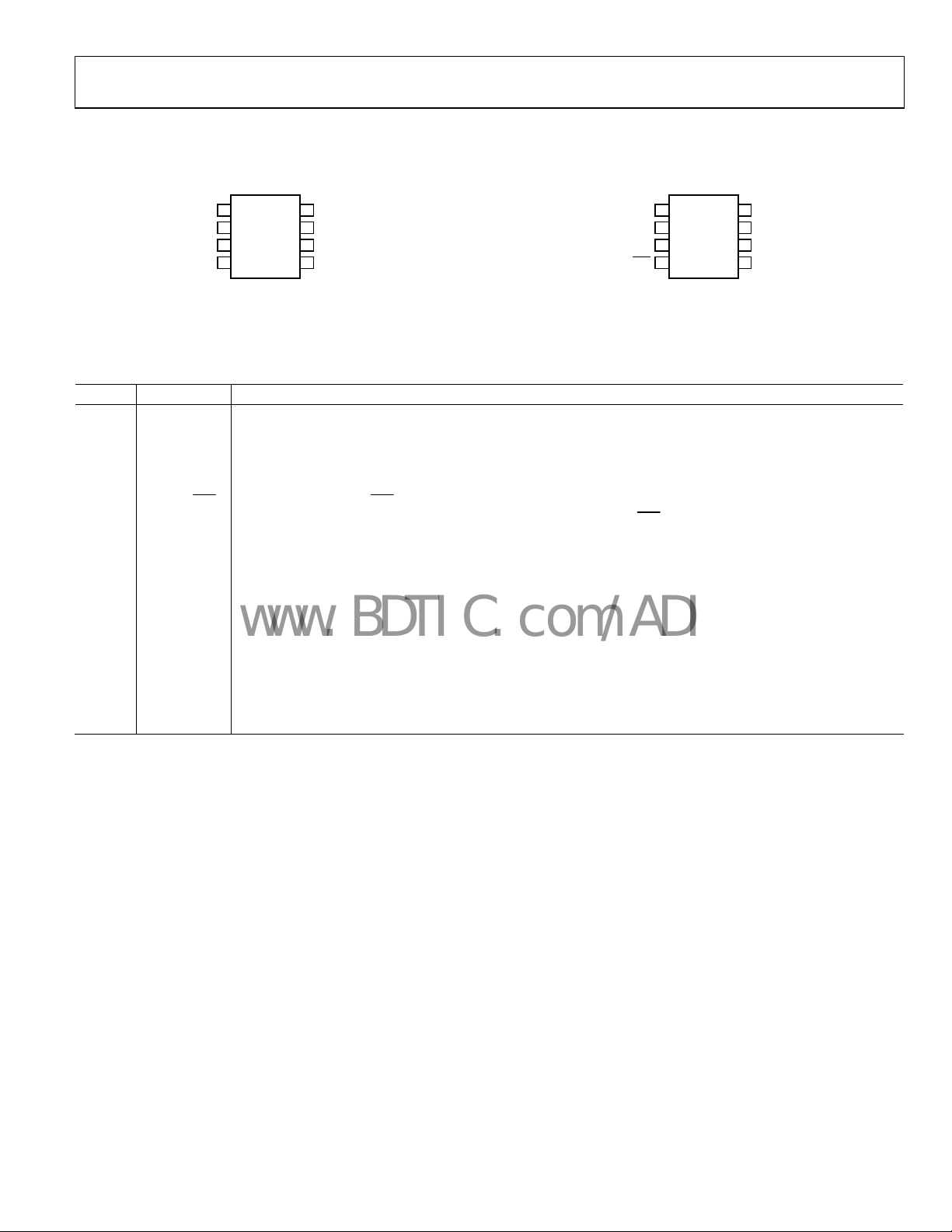
PIN CONFIGURATIONS AND FUNCTION DESCRIPTIONS
ADM1172-1AUJ
TIMER
GND
PFO
ON
1
2
TOP VIEW
(Not to Scale)
3
4
8
7
6
5
V
CC
SENSE
PFI
GATE
Figure 2. Pin Configuration, 1AUJ Model Figure 3. Pin Configuration, 2AUJ Model
Table 4. Pin Function Descriptions
Pin No. Mnemonic Description
1 TIMER
Timer Input Pin. The initial and circuit breaker timing cycles a
delay is 272.9 ms/F, and 21.7 ms/µF for a circuit breaker delay. When the TIMER pin is pulled beyond the upper
threshold, the GATE turns off.
2 GND Chip Ground Pin.
3 PFO
4
ON (ON-CLR) Input Pin. The ON (ON-CLR) pin is an input to a comparator that has a low-to-high threshold of 1.3 V with 80 mV
Power-Fail Comparator Output. Digital output from the power-fail comparator.
hysteresis and a glitch filter. The ADM1172 is reset when the ON (ON-CLR) pin is low. When the ON (ON-Error!)
pin is high, the ADM1172 is enabled. A rising edge on this pin has the added function of clearing a fault and
restarting the device on the latched off model, the ADM1172-2.
5 GATE
Gate Output Pin. An internal charge pump provides a 12 µA pull-up current to drive the gate of an N-channel
MOSFET. In an overcurrent condition, the ADM1172 controls the external FET to maintain a constant load
current.
6 PFI
7 SENSE
Power-Fail Comparator Input. Comparator threshold = 0.6 V.
Current Limit Sense Input Pin. The current limit is set via a sense resistor between the V
overcurrent condition, the gate of the FET is controlled to maintain the SENSE voltage at 50 mV. When this limit is
reached, the TIMER circuit breaker mode is activated. The circuit breaker limit can be disabled by connecting the
V
pin and SENSE pin together.
CC
8 V
CC
Positive Supply Input Pin. The ADM1172 operates between 2.7
circuit with a glitch filter resets the ADM1172 when the supply voltage drops below the specified UVLO limit.
DM1172-2AUJ
TIMER
1
2
GND
PFO
05126-006
ON-CLR
TOP VIEW
(Not to Scale)
3
4
8
7
6
5
V
CC
SENSE
PFI
GATE
re set by this external capacitor. The initial timing
and SENSE pins. In an
CC
V to 16.5 V. An undervoltage lockout (UVLO)
05126-007
Rev. 0 | Page 5 of 16
Page 6

ADM1172
www.BDTIC.com/ADI
TYPICAL PERFORMANCE CHARACTERISTICS
0.50
0.45
0.40
0.35
0.30
0.25
0.20
0.15
SUPPLY CURRENT (mA)
0.10
0.05
0
018
2 4 6 8 10121416
SUPPLY VOLTAGE (V)
Figure 4. Supply Current vs. Supply Voltage (GATE Off)
05126-023
2.65
VCC = 5V
2.63
2.61
2.59
2.57
2.55
2.53
2.51
UVLO THRESHOLD (V)
2.49
2.47
2.45
–50 150
–25 0 25 50 75 100 125
TEMPERATURE (°C)
VCC RISING
VCC FALLING
Figure 7. UVLO Threshold vs. Temperature
05126-046
0.8
0.7
0.6
0.5
0.4
0.3
SUPPLY CURRENT ( mA)
0.2
0.1
0
01
2 4 6 8 10 12 14 16
SUPPLY VOLTAGE (V)
8
05126-024
Figure 5. Supply Current vs. Supply Voltage (GATE On)
1.0
0.9
0.8
0.7
0.6
0.5
0.4
0.3
SUPPLY CURRENT ( mA)
0.2
0.1
0
–50 150
–25 0 25 50 75 100 125
VCC = 12V
VCC = 5V
TEMPERATURE (°C)
VCC = 15V
VCC = 3V
05126-033
Figure 6. Supply Current vs. Temperature
25
20
15
10
GATE VOLTAGE (V)
5
0
018
2 4 6 8 10 12 14 16
Figure 8. GATE Voltage vs. Supply Voltage
25
20
15
10
GATE VOLTAGE (V)
5
0
–50 150
–25 0 25 50 75 100 125
Figure 9. GATE Voltage vs. Temperature
SUPPLY VOLTAGE (V)
VCC = 15V
VCC = 12V
VCC = 5V
VCC = 3V
TEMPERATURE (°C)
05126-013
05126-015
Rev. 0 | Page 6 of 16
Page 7

ADM1172
–
–
www.BDTIC.com/ADI
10
9
8
7
6
5
4
3
DELTA GATE VOLTAGE (V)
2
1
0
01
2 4 6 8 10 12 14 16
SUPPLY VOLTAGE (V)
8
05126-014
Figure 10. Delta GATE Voltage vs. Supply Voltage Figure 13. I
0
VCC = 5V
–1
–2
–3
–4
(µA)
–5
–6
TIMERUP
I
–7
–8
–9
–10
–50 150
–25 0 25 50 75 100 125
TEMPERATURE (°C)
(In Initial Cycle) vs. Temperature
TIMERUP
05126-038
10
9
VCC = 12V
8
7
6
5
4
3
DELTA GATE VOLTAGE (V)
2
1
0
–50 150
–25 0 25 50 75 100 125
TEMPERATURE (°C)
VCC = 5V
VCC = 15V
VCC = 3V
05126-016
Figure 11. Delta GATE Voltage vs. Temperature Figure 14. I
0
TA = 25°C VCC = 5V
–1
–2
–3
–4
(µA)
–5
–6
TIMERUP
I
–7
–8
–9
–10
01
2 4 6 8 10 12 14 16
SUPPLY VOLTAGE (V)
Figure 12. I
(In Initial Cycle) vs. Supply Voltage
TIMERUP
8
05126-035
20
TA = 25°C
–30
–40
–50
(µA)
–60
TIMERUP
I
–70
–80
–90
–100
01
2 4 6 8 10 12 14 16
TIMERUP
20
–30
–40
–50
(µA)
–60
TIMERUP
I
–70
–80
–90
–100
–50 150
–25 0 25 50 75 100 125
Figure 15. I
TIMERUP
SUPPLY VOLTAGE (V)
(During Cct Breaker Delay) vs. Supply Voltage
TEMPERATURE (°C)
(During Cct Breaker Delay) vs. Temperature
8
05126-036
05126-039
Rev. 0 | Page 7 of 16
Page 8

ADM1172
www.BDTIC.com/ADI
3.0
TA = 25°C
2.8
2.6
2.4
2.2
(µA)
2.0
1.8
TIMERDN
I
1.6
1.4
1.2
1.0
01
2 4 6 8 10 12 14 16
Figure 16. I
1.38
VCC = 5V
1.36
34
1.
1.32
1.30
1.28
1.26
TIMER HIGH THRESHOLD ( V )
1.24
1.22
–50 150
8
SUPPLY VOLTAGE (V)
(In Cool-Off Cycle) vs. Supply Voltage Figure 19. TIMER High Threshold vs. Temperature
TIMERDN
05126-034
–25 0 25 50 75 100 125
TEMPERATURE (°C)
05126-044
3.0
VCC = 5V
2.8
2.6
2.4
2.2
(µA)
2.0
1.8
TIMERDN
I
1.6
1.4
1.2
1.0
–50 150
–25 0 25 50 75 100 125
TEMPERATURE (°C)
Figure 17. I
1.38
TA = 25°C VCC = 5V
1.36
1.34
1.32
1.30
1.28
(In Cool-Off Cycle) vs. Temperature Figure 20. TIMER Low Threshold vs. Supply Voltage
TIMERDN
05126-037
0.24
TA = 25°C
0.23
0.22
0.21
0.20
0.19
0.18
TIMER LOW THRESHOLD (V)
0.17
0.16
01
2 4 6 8 10 12 14 16
SUPPLY VOLTAGE (V)
0.24
0.23
0.22
0.21
0.20
0.19
8
05126-043
1.26
TIMER HIGH THRESHOLD ( V )
1.24
1.22
01
2 4 6 8 10 12 14 16
SUPPLY VOLTAGE (V)
Figure 18. TIMER High Threshold vs. Su
pply Voltage
8
05126-042
Rev. 0 | Page 8 of 16
0.18
TIMER LOW THRESHOLD (V)
0.17
0.16
–50 150
–25 0 25 50 75 100 125
TEMPERATURE (°C)
Figure 21. TIMER Low Threshold vs. Temperature
05126-045
Page 9

ADM1172
www.BDTIC.com/ADI
1.45
1.40
TA = 25°C
80
70
1.35
1.30
1.25
1.20
1.15
ON (ON-CLR) P IN THRESHOL D ( V )
1.10
1.05
01
2 4 6 8 10 12 14 16
Figure 22. ON (ON-
1.45
VCC = 5V
1.40
1.35
1.30
1.25
1.20
1.15
ON (ON-CLR) P IN THRESHOL D ( V )
1.10
1.05
–50 150
–25 0 25 50 75 100 125
Figure 23. ON (ON-
HIGH THRESHO L D
LOW THRESHOLD
SUPPLY VOLTAGE (V)
CLR
) Pin Threshold vs. Supply Voltage
HIGH THRESHO LD
LOW THRESHOLD
TEMPERATURE (°C)
CLR
) Pin Threshold vs. Temperature
8
05126-040
05126-041
60
50
(µs)
40
30
OFF(ONLOW)
t
20
10
0
–50 150
VCC = 15V
VCC = 3V
–25 0 25 50 75 100 125
Figure 25. t
50
49
48
47
46
(mV)
45
CB
V
44
43
42
41
40
01
2 4 6 8 10 12 14 16
Figure 26. Cct Breaker Voltage vs. Supply Voltage
VCC = 5V
TEMPERATURE (°C)
vs. Temperature
OFF(ONLOW)
SUPPLY VOLTAGE (V)
VCC = 12V
05126-048
8
05126-049
80
TA = 25°C
70
60
50
(µs)
40
30
OFF(ONLOW)
t
20
10
0
01
2 4 6 8 10 12 14 16
SUPPLY VOLTAGE (V)
Figure 24. t
OFF(ONLOW)
vs. Supply Voltage
8
05126-047
50
45
40
35
30
(mV)
25
CB
V
20
15
10
5
0
–50 150
–25 0 25 50 75 100 125
Figure 27. Cct Breaker Voltage vs. Temperature
Rev. 0 | Page 9 of 16
TEMPERATURE (°C)
05126-021
Page 10

ADM1172
–
–
–
www.BDTIC.com/ADI
12
0.620
10
8
6
4
GATE CURRENT (mA)
2
0
01
2 4 6 8 10 12 14 16
SUPPLY VOLTAGE (V)
8
05126-008
0.615
0.610
0.605
0.600
0.595
PFI THRESHOLD (V)
0.590
0.585
0.580
018
246810121416
HIGH THRESHOLD
LOW THRESHOLD
SUPPLY VOLTAGE (V)
Figure 28. GATE Current (Down) vs. Supply Voltage Figure 31. PFI Threshold vs. Supply Voltage
8
–9
–10
–11
–12
GATE CURRENT (µ A)
PFI THRESHOLD (V)
0.610
0
.605
0.600
0.595
0.590
HIGH THRESHOLD
LOW THRESHOLD
05126-025
–13
–14
01
2 4 6 8 10 12 14 16
SUPPLY VOLTAGE (V)
8
05126-009
0.585
0.580
–50 150
050100
TEMPERATURE (°C)
Figure 29. GATE Current (Up) vs. Supply Voltage Figure 32. PFI Threshold vs. Temperature
11.0
–11.2
–11.4
–11.6
–11.8
–12.0
–12.2
GATE CURRENT (µ A)
–12.4
–12.6
–12.8
–13.0
VCC = 5V
VCC = 15V
–50 150
–25 0 25 50 75 100 125
TEMPERATURE (°C)
VCC = 3V
VCC = 12V
05126-017
3.0
–3.5
–4.0
–4.5
–5.0
–5.5
–6.0
–6.5
PFO PULL -UP CURRENT (µA)
–7.0
–7.5
–8.0
–50 150
VCC = 5V
VCC = 3V
VCC = 15V
VCC = 12V
0 50 100
TEMPERATURE (°C)
Figure 30. GATE Current (up) vs. Temperature Figure 33. PFO Pull-Up Current v
05126-026
05126-027
s. Temperature
Rev. 0 | Page 10 of 16
Page 11

ADM1172
www.BDTIC.com/ADI
0.25
0.14
0.20
VCC = 3V
0.15
(V)
OL
0.10
PFO V
VCC = 5V
0.05
0
–50 150
0 50 100
TEMPERATURE (°C)
VCC = 12V
VCC = 15V
I = 300µA
s. Temperature, I = 300 μA
0.50
0.45
0.40
0.35
0.30
(V)
OL
0.25
0.20
PFO V
0.15
0.10
0.05
0
Figure 35. PFO Output Low Voltage v
VCC = 3V
VCC = 12V
VCC = 15V
–50 150
0 50 100
TEMPERATURE (°C)
VCC = 5V
I = 500µA
s. Temperature, I = 500 μA
0.12
0.10
(V)
0.08
OL
0.06
PFO V
0.04
0.02
0
–50 150
05126-028
Figure 36. PFO Output Low Voltage v
700
600
500
400
(mV)
OL
300
PFO V
200
100
0
–0.1 1.1
05126-029
VCC = 3V
VCC = 12V
0 50 100
TEMPERATURE (°C)
VCC = 5V
VCC = 15V
s. Temperature, I = 100 μA Figure 34. PFO Output Low Voltage v
VCC = 3V
VCC = 12V
VCC = 15V
VCC = 5V
0.1 0.3 0.5 0.7 0.9
(mA)
I
LOAD
I = 100µA
05126-030
05126-031
Figure 37. PFO Output Low Voltage vs. Load Current
Rev. 0 | Page 11 of 16
Page 12

ADM1172
www.BDTIC.com/ADI
THEORY OF OPERATION
Many systems require the insertion or removal of circuit boards
to live backplanes. During this event, the supply bypass and holdup capacitors can require substantial transient currents from the
backplane power supply as they charge. These currents can
cause permanent damage to connector pins or undesirable glitches
and resets to the system.
The ADM1172 is intended to control the powering of a system
n and off) in a controlled manner, allowing the board to be
(o
removed from, or inserted into, a live backplane by protecting it
from excess currents. The ADM1172 can reside either on the
backplane or on the removable board.
OVERVIEW
The ADM1172 operates over a supply range of 2.7 V to 16.5 V.
As the supply voltage is coming up, an undervoltage lockout
circuit checks if sufficient supply voltage is present for proper
operation. During this period, the FET is held off by the GATE
pin being held to GND. When the supply voltage reaches a level
above UVLO and the ON (ONcycle ensures that the board is fully inserted in the backplane
before turning on the FET. The TIMER pin capacitor sets the
periods for all of the TIMER pin functions. After the initial
timing cycle, the ADM1172 monitors the inrush current
through an external sense resistor. Overcurrent conditions are
actively limited to 50 mV/R
limit. The ADM1172-1 automatically retries after a current
limit fault and the ADM1172-2 latches off. The retry duty cycle
on the ADM1172-1 timer function is limited to 3.8% for FET
cooling.
CLR
) pin is high, an initial timing
for the circuit breaker timer
SENSE
delay time at card insertion. If using a short pin system to
enable the device, a pull-down resistor should be used to hold
the device prior to insertion.
GATE
Gate drive for the external N-channel MOSFET is achieved
using an internal charge pump. The gate driver consists of a
12 A pull-up from the internal charge pump. There are various
pull-down devices on this pin. At a hotswap condition the board
is hot inserted to the supply bus. During this event, it is possible
for the external FET GATE capacitance to be charged up by the
sudden presence of the supply voltage. This can cause
uncontrolled inrush currents. An internal strong pull-down
circuit holds GATE low while in UVLO. This reduces current
surges at insertion. After the initial timing cycle, the GATE is
then pulled high. During an overcurrent condition, the
ADM1172 servos the GATE pin in an attempt to maintain a
constant current to the load until the circuit breaker timeout
completes. In the event of a timeout, the GATE pin abruptly
shuts down using the 4 mA pull-down device. Care must be
taken not to load the GATE pin resistively because this reduces
the gate drive capability.
CURRENT LIMIT FUNCTION
The ADM1172 features a fast response current control loop that
actively limits the current by reducing the gate voltage of the
external FET. This current is measured by monitoring the
voltage drop across an external sense resistor. The ADM1172
tries to regulate the gate of the FET to achieve a 50 mV voltage
drop across the sense resistor.
UVLO
If the VCC supply is too low for normal operation, an undervoltage lockout circuit holds the ADM1172 in reset. The GATE
pin is held to GND during this period. When the supply reaches
this UVLO voltage, the ADM1172 starts when the ON (ONpin condition is satisfied.
CLR
)
ON (ON-CLR) PIN
The ON (ONcomparator that has a low-to-high threshold of 1.3 V with 80 mV
hysteresis and a glitch filter. The ADM1172 is reset when the
ON (ONthe ADM1172 is enabled. A rising edge on this pin has the
added function of clearing a fault and restarting the device on
the latched off model, the ADM1172-2. A low input on the ON
CLR
(ONpin to ground and resets the timer. An external resistor divider at
the ON (ONlockout value higher than the internal UVLO circuit. There is a
glitch filter delay of approximately 3 s on rising allowing the
addition of an RC filter at the ON (ON-
CLR
) pin is the enable pin. It is connected to a
CLR
) pin is low. When the ON (ON-
) pin turns off the external FET by pulling the GATE
CLR
) pin can be used to program an undervoltage
CLR
) pin is high,
CLR
) pin to increase the
Rev. 0 | Page 12 of 16
CALCULATING THE CURRENT LIMIT
The sense resistor connected between VCC and the SENSE pin is
used to determine the nominal fault current limit. This is given
by the following equation:
ILIMIT
The minimum load current is given by Equation 2
ILIMIT
The maximum load current is given by Equation 3.
ILIMIT
For proper operation, the minimum current limit must exceed
he circuit maximum operating load current with margin. The
t
sense resistor power rating must exceed
(VCB
= VCB
NOM
= VCB
MIN
= VCB
MAX
)2/RSENSE
MAX
/RSENSE
NOM
/RSENSE
MIN
/RSENSE
MAX
MIN
(1)
NOM
(2)
MAX
(3)
MIN
CIRCUIT BREAKER FUNCTION
When the supply experiences a sudden current surge, such as a
low impedance fault on load, the bus supply voltage can drop
significantly to a point where the power to an adjacent card is
affected, potentially causing system malfunctions. The
ADM1172 limits the current drawn by the fault by reducing the
Page 13

ADM1172
V
www.BDTIC.com/ADI
gate voltage of the external FET. This minimizes the bus supply
voltage drop caused by the fault and protects neighboring cards.
When the initial cycle ends, a start-up cycle activates and the
GATE pin is pulled high; the TIMER pin continues to pull down.
As the voltage across the sense resistor approaches the current
limit, a timer activates. This timer resets again if the sense
voltage returns below this level. If the sense voltage is any
voltage below 44 mV, the timer is guaranteed to be off. Should
the current continue to increase, the ADM1172 tries to regulate
the gate of the FET to achieve a limit of 50 mV across the sense
resistor. However, if the device is unable to regulate the fault
current and the sense voltage further increases, a larger pulldown, in the order of milliamperes, is enabled to compensate
for fast current surges. If the sense voltage is any voltage greater
than 56 mV, this pull-down is guaranteed to be on. When the
timer expires, the GATE pin shuts down.
TIMER FUNCTION
The TIMER pin is responsible for several key functions on the
ADM1172. A capacitor controls the initial power on reset time
and the amount of time an overcurrent condition lasts before
the FET shuts down. On the ADM1172-1, the timer pin also
controls the time between auto retry pulses. There are pull-up
and pull-down currents internally available to control the timer
functions. The voltage on the TIMER pin is compared with two
threshold voltages: COMP1 (0.2 V) and COMP2 (1.3 V). The
four timing currents are listed in
Tabl e 5.
Table 5.
Timing Current Level (μA)
Pull-up 5
Pull-up 60
Pull-down 2
Pull-down 100
POWER-UP TIMING CYCLE
CLR
The ADM1172 is in reset when the ON (ONlow. The GATE pin is pulled low and the TIMER pin is pulled
low with a 100 µA pull-down. At Time Point 2 in Figure 38, the
ON-
CLR
) pin is pulled high. For the device to startup
ON (
correctly, the supply voltage must be above UVLO, the ON
CLR
(ON-
) pin must be above 1.3 V, and the TIMER pin voltage
must be less than 0.2 V. The initial timing cycle begins when these
three conditions are met, and the TIMER pin is pulled high with
5 µA. At Time Point 3, the TIMER reaches the COMP2 threshold.
This is the end of the first section of the initial cycle. The 100 µA
c
urrent source then pulls down the TIMER pin until it reaches
0.2 V at Time Point 4. The initial cycle delay (Time Point 2 to
Time Point 4) relates to C
= 1.3 × C
t
INITIAL
TIMER
by equation
TIMER
/5 µA (4)
) pin is held
CIRCUIT BREAKER TIMING CYCLE
When the voltage across the sense resistor exceeds the circuit
breaker trip voltage, the 60 µA timer pull-up current is activated.
If the sense voltage falls below this level before the TIMER pin
reaches 1.3 V, the 60 µA pull-up is disabled and the 2 µA pulldown is enabled. This is likely to happen if the overcurrent fault
is only transient, such as an inrush current. This is shown in
Figure 39. However, if the overcurrent condition is continuous
a
nd the sense voltage remains above the circuit breaker trip
voltage, the 60 µA pull-up remains active. This allows the TIMER
pin to reach the high trip point of 1.3 V and initiate the GATE
shutdown. On the ADM1172-2, the TIMER pin continues pulling
up but switches to the 5 µA pull-up when it reaches the 1.3 V
V
TIMER
V
GATE
V
OUT
V
TIMER
V
GATE
V
I
RSENSE
V
IN
1
ON
2
RESET
MODE
Figure 38. Power-Up Timing
V
IN
V
ON
OUT
RESET
MODE
Figure 39. Power-Up into Capacitor
INITIAL
CYCLE
5µA
100µA
INITIAL
CYCLE
3
60µA
4
START-UP
CYCLE
START-UP
CYCLE
NORMAL
CYCLE
2µA
NORMAL
CYCLE
05126-002
05126-003
Rev. 0 | Page 13 of 16
Page 14

ADM1172
www.BDTIC.com/ADI
CLR
threshold. The device can be reset by toggling the ONo
r by manually pulling the TIMER pin low. On the ADM1172-1,
the TIMER pin activates the 2 µA pull-down once the 1.3 V
threshold is reached, and continues to pull down until it reaches
the 0.2 V threshold. At this point, the 100 µA pull-down is
activated and the GATE pin is enabled. The device keeps
retrying in the manner as shown in
Figure 40.
pin
The ADM1172-2 model has a latch off system whereby when a
current fault is detected, the GATE is switched off after a time
determined by the timer capacitor (see
Toggling the ON-
CLR
pin, or pulling the TIMER pin to GND
Figure 41 for details).
for a brief period, resets this condition.
I
RSENSE
The duty cycle of this automatic retry cycle is set to the ratio of
2 µA/60 µA,
which approximates 3.8% on. The value of the
timer capacitor determines the on time of this cycle. This time
is calculated as follows:
= 1.3 × C
t
ON
t
= 1.1 × C
OFF
I
RSENSE
V
TIMER
V
GSFET
V
OUT
Figure 40. ADM1172-1 Automatic Retry During Overcurrent Fault
TIMER
TIMER
/60 A
/2 A
60µA
100µA
SHORTCIRCUIT
EVENT
FAULT
CYCLE
2µA
COMP1COMP2
FAULT
CYCLE
05126-004
AUTOMATIC RETRY OR LATCHED OFF
The ADM1172 is available in two models. The ADM1172-1
has an automatic retry system whereby when a current fault is
detected, the FET is shut down after a time determined by the
timer capacitor, and it is switched on again in a controlled continuous cycle to determine if the fault remains (see
or details). The period of this cycle is determined by the timer
f
capacitor at a duty cycle of 3.8% on and 96.2% off.
Figure 40
5µA
V
TIMER
V
GSFET
V
OUT
Figure 41. ADM1172-2 Latch Off After Overcurrent Fault
60µA
SHORTCIRCUIT
EVENT
COMP1COMP2
05126-005
POWER-FAIL COMPARATOR
The ADM1172 has an integrated comparator that can be used
as a power-fail/OV/UV detector. The comparator has a 0.6 V
reference, and it is designed to be active high when the voltage
on the PFI pin drops to below this threshold. The only action
that results from the PFI pin tripping the comparator is the
change of state on the PFO pin. The PFI pin can be used to
monitor the supply on either side of the FET, for an OV or UV
condition set by a resistor divider network. The PFO can then
be sent to a control system and used as a power-good/power-fail
signal. The PFO output has a 5 µA internal pull-up. A 10 kΩ
resistor is recommended on the PFO pin to ensure that it is
either pulled up or down during power-up. The pin is in high
impedance while V
fail signals.
< UVLO and can result in invalid power-
CC
Rev. 0 | Page 14 of 16
Page 15

ADM1172
www.BDTIC.com/ADI
OUTLINE DIMENSIONS
2.90 BSC
2
1.95
BSC
56
0.65 BSC
2.80 BSC
*
1.00 MAX
SEATING
PLANE
0.20
0.08
8°
4°
0°
0.60
0.45
0.30
847
1.60 BSC
13
PIN 1
INDICATOR
*
0.90
0.87
0.84
0.10 MAX
0.38
0.22
*
COMPLIANT TO JEDEC STANDARDS MO-193-BA WITH
THE EXCEPTION OF PACKAGE HEIGHT AND THICKNESS.
Figure 42. 8-Lead Thin Small Outline Transistor Package [TSOT]
(UJ-8)
Dim
ensions shown in millimeters
ORDERING GUIDE
Model Temperature Range Package Description Package Option Branding
ADM1172-1AUJZ-RL7 8-Lead TSOT UJ-8 M1M
ADM1172-2AUJZ-RL7 8-Lead TSOT UJ-8 M1N
1
Z = Pb-free part.
1
1
−40°C to +85°C
−40°C to +85°C
Rev. 0 | Page 15 of 16
Page 16

ADM1172
www.BDTIC.com/ADI
NOTES
©2006 Analog Devices, Inc. All rights reserved. Trademarks and
registered trademarks are the property of their respective owners.
D05126-0-7/06(0)
Rev. 0 | Page 16 of 16
 Loading...