

Page 1
Dual, USB 2.0 Full/Standby Power
=
Preliminary Technical Data
FEATURES
500mA Load Current (100mA in Standby Mode)
135m⍀ On Resistance
Switchable Current Limit
50µA Typical Quiescent Current
10nA Typical Shutdown Current
40nA Typical Switch Off Leakage
Short-Circuit Protection
Thermal Shutdown
FLT Outputs
Small, 16-Pin QSOP Package
APPLICATIONS
Desktop Computers
Palmtop Computers
Notebook Computers
Hand-Held Instruments
Universal Serial Bus (USB)
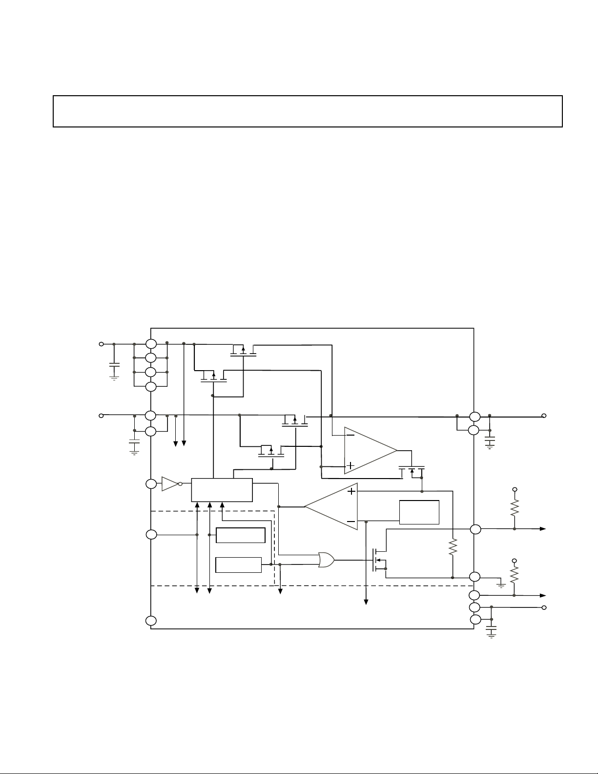
1A MIRROR
FET
1A MAIN FET
MAIN_IN
(2.7V TO 5.5V)
22µF
2
3
14
15
Controller with Supply Steering
ADM1072
GENERAL DESCRIPTION
The ADM1072 is a logic controlled, dual P-channel switch
with low on resistance and a built-in current limiter, capable of
sourcing up to 1A from supply voltages between 2.7V and
5.5V. In addition to logic inputs that switch each channel on
and off, the device has a standby input that switches the output
current limit, making it ideal for use with USB peripherals. In
normal operating mode and Standby mode the output current
is typically limited to 500mA and 100mA respectively, as
outlined by the USB2.0 Specification. This allows the system
power supply to be protected against short-circuits and surge
currents in peripheral USB devices powered via the ADM1072.
Over-current and over-temperature conditions are signalled by
a fault output (FLT) for each channel.
The ADM1072 also offers low quiescent current of typically
50µA and shutdown current of typically 10nA.
STBY_IN
(2.7V TO
5.5V)
Rev. PrE 1/02
4.7µF
ON1
STBY
ON2
5
12
11
9
10
TO
CHANNEL 2
TO
CHANNEL
2
0.2A MAIN FET
0.2A
MIRROR FET
CONTROL
LOGIC
UNDERVOLTAGE
SENSOR
TEMPERATURE
SENSOR
CHANNEL
CHANNEL 2 IS IDENTICAL TO CHANNEL 1
ADM1072
OVERTEMP
TO
2
CURRENT
AMPLIFIER
FUNCTIONAL BLOCK DIAGRAM
AMPLIFIER
LIMIT
TO
CHANNEL
2
MIRROR
1.24V
BANDGAP
REFERENCE
CURRENT
SETTING
RESISTOR
1
4
120µF
V
PULLUP
0 TO
5.5V
R
10k⍀ TO
FLT1
6
V
PULLUP
0 TO 5.5V
GND
8
FLT2
7
13
16
120µF
R
10k⍀ TO 100k⍀
OP1
PULLUP
100k⍀
PULLUP
OP2
Information furnished by Analog Devices is believed to be accurate and
reliable. However, no responsibility is assumed by Analog Devices for its
use, nor for any infringements of patents or other rights of third parties
which may result from its use. No license is granted by implication or
otherwise under any patent or patent rights of Analog Devices.
One Technology Way, P.O. Box 9106, Norwood, MA 02062-9106, U.S.A.
Tel: 781/329-4700 World Wide Web Site: http://www.analog.com
Fax: 781/326-8703 © Analog Devices, Inc., 2002
Page 2

ADM1072–SPECIFICATIONS
(Specification for either channel 1 or channel 2, VIN = +5.0V, TA = -40 to +85oC, unless otherwise noted.)
Parameter Min Typ Max Units Test Conditions/Comments
Operating Voltage Range +2.7 +5.5 Volts
Quiescent Current (Total Device) 50 µA VIN = 5V, ON1,ON2 = GND, I
Shutdown Supply Current (Total Device) 0.01 2 µA ON1,ON2 = VIN = 5.5V, V
Undervoltage Lockout 2.0 2.3 2.6 V V
On Resistance ? 135 m⍀ V
, Rising Edge, 1% Hysteresis
STBY_IN
= 4.75V
IN
?? m⍀ VIN = 3.0V
NOMINAL CURRENT-LIMIT
Full Power Mode 0.8 1.0 1.2 A STBY Low Note 1
Standby Mode 160 200 240 mA STBY High Note 1
ON1,ON2, STBY Input Low Voltage, V
IL
0.8 V VIN = 2.7V to 5.5V
ON1,ON2, STBY Input High Voltage, VIH2.4 V VIN = 2.7V to 5.5V
ON1,ON2, STBY Input Leakage 0.01 ±1 µA V
FLT1,FLT2 Logic Output Low Voltage 0.4 V I
FLT1,FLT2 Output High Leakage Current 0.05 1 µA V
Turn-On Time 4 ms V
4msV
ON, VSTBY
SINK
FAULT
IN
IN
Turn-Off Time ? ? 20 µs VIN = 5V, I
Notes
1
Current limit is specified with V
2
Guaranteed by design. Derived from the I
3
Tested with I
4
Specifications to -40oC are guaranteed by design, not tested.
= 200mA and V
OUT
= 4.5V.
OUT
SET
current ratio, current-limit amplifier and internal set resistor accuraciues.
SET
adjusted until (VIN - V
) 艌 0.8V.
OUT
= 1mA
= 5.5V
= 5V, I
= 3V, I
= 5.5V
= 500mA
OUT
= 500mA
OUT
= 500mA
OUT
OUT
OUT
= 0V
= 0A
–2–
Rev. PrE 1/02
Page 3
ABSOLUTE MAXIMUM RATINGS*
(TA = +25°C unless otherwise noted)
MAIN_IN to GND . . . . . . . . . . . . . . . . . . . . . . –0.3V to +6V
ON1,ON1,FLT1, FLT2 to GND . . . . . . . . . . . –0.3V to +6V
OP1,OP2 to GND . . . . . . . . . . . . . . . .+0.3 V to (V
+ 0.3V)
IN
Maximum Switch Current
Full Power Mode . . . . . . . . . . . . . . . . . . . . . . . . . . . . . . . . 1A
Standby Power Mode . . . . . . . . . . . . . . . . . . . . . . . . 200mA
Continuous Power Dissipation (TA = +70
QSOP (derate 8.3mW/
o
C above +70oC)
o
C) . . . . . 667mW
Operating Temperature Range
Industrial (A Version) . . . . . . . . . . . . . . . –40°C to +85°C
Storage Temperature Range . . . . . . . . . . . –65°C to +150°C
Lead Temperature (Soldering, 10 sec) . . . . . . . . . . . +300°C
*This is a stress rating only and functional operation of the device at these or any
other conditions above those indicated in the operation sections of this specification is not implied. Exposure to absolute maximum rating conditions for
extended periods of time may affect reliability.
THERMAL CHARACTERISTICS
16-Pin QSOP Package:
q
= 105°C/Watt, q
JA
= 40°C/Watt
JC
ORDERING GUIDE
Temperature Package Package
Model Range Description Option
ADM1072ARQ -40°C to +85°C 16-Pin QSOP RQ-16
Package
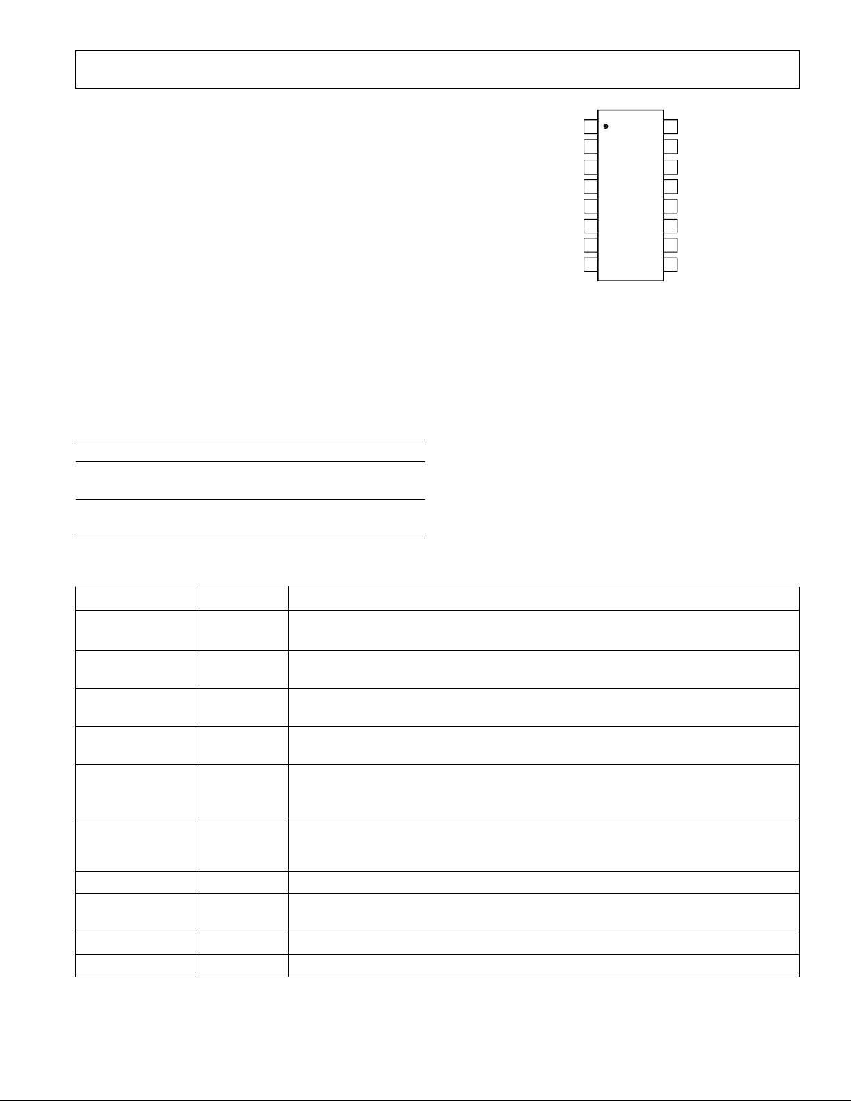
OP1
1
MAIN_IN
MAIN_IN
STBY_IN
OP1
FLT1
FLT2
GND
2
3
4
ADM10 72
TOP VIEW
5
(Not to Scale)
6
7
8
Pin Configuration
ADM1072
16
OP2
15
MAIN_IN
14
MAIN_IN
OP2
13
STBY_IN
12
ON1
11
ON2
10
STBY
9
PIN FUNCTION DESCRIPTION
Pin Mnemonic Function
2, 3, 14, 15 MAIN_IN Input to MAIN P-channel MOSFET source (both channels). Bypass MAIN_IN with a
22µF capacitor to ground.
5, 12 STBY_IN Input to Standby P-channel MOSFET source (both channels) and supply to chip
circuitry. Bypass STBY_IN with a 4.7µF capacitor to ground.
1, 4 OP1 Output from channel 1, P-channel MOSFET drains. Bypass OP1 with a 120µF capacitor
to ground.
13, 16 OP2 Output from channel 2, P-channel MOSFET drains. Bypass OP2 with a 120µF capacitor
to ground.
6 FLT1 Open-Drain Digital Output. FLT1 goes low when the channel 1 current limit is
exceeded for 10mS or the die temperature exceeds +150oC. During startup, FLT1
remains low for the turn-on time.
7 FLT2 Open-Drain Digital Output. FLT2 goes low when the channel 2 current limit is
exceeded for 10mS or the die temperature exceeds +150oC. During startup, FLT2
remains low for the turn-on time.
8 GND Ground pin for all chip circuits.
9 STBY Digital Input. Active high standby mode input. STBY = 0 sets normal operating mode
with 500mA current limit. STBY = 1 sets standby mode with 100mA current limit.
10 ON2 Digital Input. Active-low switch enable for channel 2 (logic 0 turns the switch on).
11 ON1 Digital Input. Active-low switch enable for channel 1 (logic 0 turns the switch on).
Rev. PrE 1/02
–3–
Page 4

ADM1072
Typical Performance Curves
AWAITING
TA
DA
Figure 1. Quiescent Current vs. Input Voltage
AWAITING
TA
DA
Figure 2. Quiescent Current vs. Temperature
AWAITING
TA
DA
Figure 4. Off-Switch Current vs. Temperature
AWAITING
TA
DA
Figure 5. Normalized On Resistance vs. Temperature
AWAITING
TA
DA
Figure 3. Off-Supply Current vs. Temperature
AWAITING
TA
DA
Figure 6. I
–4–
Ratio vs Switch Current
OUT/ISET
Rev. PrE 1/02
Page 5

Typical Performance Curves
ADM1072
AWAITING
TA
DA
Figure 7. Normalized Output Current vs. Output Voltage
AWAITING
TA
DA
Figure 8. Turn-On Time vs. Temperature
AWAITING
TA
DA
Figure 10. Fast Current-Limit Response
AWAITING
TA
DA
Figure 11. Slow Current-Limit Response
AWAITING
Figure 9. Turn-Off Time vs. Temperature
Rev. PrE 1/02
DA
TA
AWAITING
TA
DA
Figure 12. Load Transient Response
–5–
Page 6

ADM1072
Typical Performance Curves
AWAITING
TA
DA
Figure 13. Switch Turn-On Time
AWAITING
TA
DA
Figure 14. Switch Turn-Off Time
AWAITING
TA
DA
Figure 15. USB Circuit Output Rise Time
AWAITING
TA
DA
Figure 16 USB Circuit output Fall Time
–6–
Rev. PrE 1/02
Page 7

ADM1072
FUNCTIONAL DESCRIPTION
The ADM1072 is a dual, logic-controlled P-channel switch.
Each channel of the ADM1072 comprises two P-channel
switches. The source of one switch is connected to the
“MAIN_IN” input pins and can switch up to 1A. The second
switch is conected to the “STBY_IN” pins and can switch up to
200mA. The device is rated to provide 500mA continuously in
full power mode and 100mA continuously in STBY mode. The
STBY_IN inputs also provide the power for the chip circuitry
and so must be connected to a supply at all times.
When STBY is low the MAIN switch is active and when STBY
is high the Standby switch is active.
Each channel is individually controlled by an active-low logic
input ON1 (pin 11) and ON2 (pin 10). When either ON1 or
ON2 is low, the internal circuitry of the ADM1072 is powered
up and the output of the corresponding current-limit amplifier
is low, providing gate drive to the switching FET, thus turning
it on. When both ON inputs are high, the internal circuitry is
powered down and the current consumption is typically 10nA.
It should be noted that the ADM1072 is not a bi-directional
switch, so V
must always be higher than V
IN
OUT
.
TABLE 1. Truth Table for ON1, ON2 and STBY
ON1 ON2 STBY Channel 1 Channel 2
0 0 0 500mA 500mA
0 0 1 100mA 100mA
0 1 0 500mA OFF
0 1 1 100mA OFF
1 0 0 OFF 500mA
1 0 1 OFF 100mA
SHORT-CIRCUIT PROTECTION
The proportional relationship between the main FET and the
mirror FET is only maintained down to an output voltage of
about 1.6V. Below this voltage the output current is limited to
approximately 1.2 x I
LIMIT
.
In the event of a high dV/dt across the switching FET during a
short-circuit, the switch will turn off and disconnect the input
from the output. The switch is then turned on slowly with the
current limited to the short-circuit value.
THERMAL SHUTDOWN
The thermal shutdown operates when the die temperature
exceeds +150
down circuit has built-in hysteresis of 10
not turn on again until the die temperature falls to +140
o
C, turning off both channels. The thermal shut-
o
C, so the switch will
o
C. If
the fault condition is not removed, the switch will pulse on and
off as the temperature cycles between these limits.
UNDERVOLTAGE LOCKOUT
The undervoltage sensor monitors the input supply voltage (ie)
the voltage on STBY_IN. The outputs will not turn on until
the supply voltage is sufficient for the chip circuits to operate
reliably. Undervoltage lockout occurs at between 2.0 and 2.6V.
FLT OUTPUTS
The ADM1072 has active-low fault outputs for each channel,
FLT1 (pin 6) and FLT2 (pin 7). If the current limit is
exceeded for greater than 10mS, the corresponding FLT
output will pull low. If the thermal shutdown is activated, both
FLT outputs will pull low. The FLT outputs are open-drain
and require a pullup resistor of between 10k⍀ and 100k⍀.
Several FLT outputs may be wire-OR’d to form a common
interrupt line, as shown in Figure 17 or FLT outputs may be
wire-OR’d to an existing interrupt line that has a resistive pullup.
V
PULLUP
1 1 X BOTH SHUT DOWN
X = don’t care
CURRENT LIMIT
When either the Main or Standby switch is turned on a smaller
mirror switch passes a proportionate current equal to I
OUT
/
1000. The mirror amplifier maintains this relationship by
keeping the drain of the mirror FET at the same voltage as the
main FET, and drives the mirror current through an internal
current-limit resistor, which is connected between the noninverting input of the current limit amplifier and ground. An
on-chip bandgap reference of 1.24V is connected to the
inverting input of the current-limit amplifier. When the load
current exceeds the preset limit, the voltage across the currentlimit resistor exceeds 1.24V and the output voltage of the current-limit amplifier rises, reducing the gate drive to the FETs.
By selecting between the Standby and Main FETs and their
associated mirror FETs, the STBY input allows the two different values of current limit specified by USB2.0 to be selected.
This feature is particularly useful when driving USB peripherals
from a host system such as a PC that can go into a powersaving mode, since it limits the current that the peripherals can
attempt to draw from the host power supply.
Rev. PrE 1/02
–7–
R
PULLUP
INT
FLT1
ADM1072
FLT2
FLT1
ADM1072
FLT2
FLT1
ADM1072
FLT2
Figure 17. Wire Or’ing FAULT Outputs
During startup, the FLT output goes low for the turn-on time.
Page 8

ADM1072
APPLICATIONS INFORMATION
INPUT FILTERING
To prevent the input voltage being pulled below the minimum
operating voltage under transient short-circuit conditions,
before the current limit has had time to operate, a reservoir
capacitor should be connected from MAIN_IN to GND. This
does not need to be large, but should have a low ESR. A value
of around 10 - 22µF is suitable. Larger values will reduce the
voltage drop still further. The STBY_IN input requires a
proportionately smaller value, typically 2.2 to 4.7µF.
OUTPUT CAPACITANCE
120µF capacitors should be connected between OP1 and OP2
and GND to prevent the back e.m.f. of parasitic inductance
from pulling OP1 and OP2 below ground during turn-off and
to provide adequate turn- on current for Universal Serial Bus
(USB) applications that are hot plugged to OP! or OP2. This
causes the output rise and fall times to be longer, as shown in
the typical operating characteristics, but does not affect the
turn-off time of the ADM1072 itself.
LAYOUT CONSIDERATIONS
Printed circuit board tracks to and from the ADM1072 should
be as thick and as short as possible to minimise parasitic inductance and take full advantage of the fast response time of the
switch. Input and output capacitors should be placed as close
to the device as possible (less than 5mm).
THERMAL CONSIDERATIONS
Under normal operating conditions, the worst-case power
dissipation will be 135mW with the 135m⍀ on resistance and
3V supply (W = (1A)
2
⫻ 0.135⍀). The package is capable of
handling and dissipating this power, but heat dissipation can
further be improved by providing a large area of copper in
contact with the device pins, particularly MAIN_IN and
OP1,OP2.
OUTLINE DIMENSIONS
Dimensions shown in inches and (mm).
16-Pin QSOP Package (RQ-16)
0.197 (5.00)
0.189 (4.80)
9
0.244 (6.20)
0.228 (5.79)
8
0.069 (1.75)
0.053 (1.35)
0.157 (3.99)
0.150 (3.81)
0.059 (1.50)
16
1
PIN 1
MAX
0.010 (0.25)
0.004 (0.10)
0.025
(0.64)
BSC
0.012 (0.30)
0.008 (0.20)
SEATING
PLANE
–8–
0.010 (0.20)
0.007 (0.18)
8
&
0
&
0.050 (1.27)
0.016 (0.41)
Rev. PrE 1/02
 Loading...