

Page 1
Thermal Monitor and
FEATURES
1 local and 2 remote temperature channels
±1°C accuracy on local and remote channels
Automatic remote temperature channels, up to 1 kΩ
Fast (up to 64 measurements per second)
SMBus 2.0, 1.1, and 1.0 compliant
SMBus address input/LOCATION input to UDID
Programmable over-/undertemperature limits
Programmable fault queue
SMBusALERT
Fail-safe overtemperature comparator output
Fan speed (RPM) controller
DRIVE1
DRIVE2
output
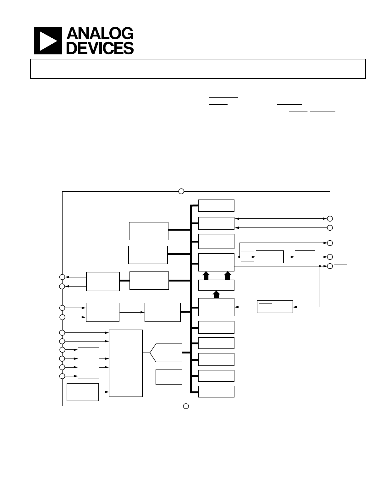
ADM1034
1
3
FAN SPEED
CONTROLLER
FUNCTIONAL BLOCK DIAGRAM
MANUAL FAN
SPEED CONTROL
REGISTERS
TEMPERATURE-TO-
FAN-SPEED
LOOK-UP TABLE
FAN RESPONSE
Fan Speed (RPM) Controller
ADM1034
Look-up table for temperature-to-fan-speed control
Linear and discrete options for look-up table
FAN _FA ULT
THERM
REF input, used as reference for
3 V to 5.5 V supply
Small 16-lead QSOP package
APPLICATIONS
Desktop and notebook PCs
Embedded systems
Telecommunications equipment
LCD projectors
V
CC
6
SMBUS
ADDRESS
SERIAL BUS
INTERFACE
ADDRESS
POINTER
REGISTER
STATUS
REGISTER
LIMIT
COMPARATOR
output
input, used to time
ALERT
THERM
MASK
REGISTERS
PROCHOT
assertions
THERM (PROCHOT
FAULT
QUEUE
)
16
SCL
15
SDA
8
FAN_FAULT
14
ALERT
7
THERM
2
TACH1
4
TACH2
8
REF
D1–
D1+
D2–
D2+
13
9
10
11
12
TEMPERATURE
LOCATION
Rev. 0
Information furnished by Analog Devices is believed to be accurate and reliable.
However, no responsibility is assumed by Analog Devices for its use, nor for any
infringements of patents or other rights of third parties that may result from its use.
Specifications subject to change without notice. No license is granted by implication
or otherwise under any patent or patent rights of Anal og Devices. Trademarks and
registered trademarks are the property of their respective owners.
SRC
BLOCK
BAND GAP
SENSOR
TACH SIGNAL
CONDITIONING
ANALOG
MULTIPLEXER
FAN
SPEED
COUNTER
ADC
BAND GAP
REFERENCE
GND
5
Figure 1.
VALUE AND
LIMIT
REGISTERS
FAULT
QUEUE
HYSTERESIS
REGISTERS
OFFSET
REGISTERS
CONVERSION
RATE REGISTER
CONFIGURATION
REGISTERS
THERM PERCENT
TIMER
One Technology Way, P.O. Box 9106, Norwood, MA 02062-9106, U.S.A.
Tel: 781.329.4700
Fax: 781.326.8703 © 2004 Analog Devices, Inc. All rights reserved.
www.analog.com
04918-0-001
Page 2

ADM1034
TABLE OF CONTENTS
Specifications..................................................................................... 4
Interrupt Behavior ....................................................... 21
ALERT
Absolute Maximum Ratings............................................................ 6
Thermal Characteristics .............................................................. 6
ESD Caution.................................................................................. 6
Pin Configuration and Function Descriptions............................. 7
Typical Performance Characteristics............................................. 8
Functional Description ..................................................................10
Internal Registers ........................................................................ 10
Serial Bus Interface..................................................................... 10
Location Input.............................................................................10
SMBus 2.0 ARP-Capable Mode................................................ 10
SMBus 2.0 Fixed-and-Discoverable Mode.............................. 12
SMBus 2.0 Read and Write Operations ...................................12
Register Addresses for Single/Block Byte Modes ...................14
Write Operations ........................................................................ 14
Read Operations ......................................................................... 15
SMBus Timeout ..........................................................................15
Packet Error Checking (PEC)................................................... 15
Alert Response Address (ARA)................................................ 15
Temperature Measurement System.............................................. 16
Internal Temperature Measurement........................................ 16
Remote Temperature Measurement......................................... 16
Additional Functions ................................................................. 18
Handling
Interrupt Masking Register ....................................................... 22
FAN_ FAULT
Fault Queue ................................................................................. 23
Conversion Rate Register.......................................................... 23
THERM
THERM
Fan Drive Signal ......................................................................... 25
Synchronous Speed Control ..................................................... 25
Fan Inputs .................................................................................... 26
Fan Speed Measurement ........................................................... 26
Fan Speed Measurement Registers........................................... 27
Reading Fan Speed ..................................................................... 27
Calculating Fan Speed ............................................................... 27
Alarm Speed................................................................................ 27
Look-Up Table: Modes of Operation....................................... 28
Setting Up the Size of the Look-Up Table............................... 29
Setting Up the Look-Up Table in Linear Mode...................... 29
Setting Which Temperature Channel Controls a Fan ........... 29
Look-Up Table Hysteresis ......................................................... 29
Programming the
Channel
SMBUSALERT
Output ................................................................. 23
I/O Timer and Limits ................................................ 23
% Limit Register ......................................................... 24
........................................................................................ 30
Interrupts ....................................... 22
THERM
Limit for Each Temperature
Layout Considerations................................................................... 19
Limits, Status Registers, and Interrupts ....................................... 20
8-Bit Limits.................................................................................. 20
Out-of-Limit Comparisons .......................................................20
Analog Monitoring Cycle Time................................................ 20
Status Registers ........................................................................... 20
REVISION HISTORY
8/04—Revision 0: Initial Version
Rev. 0 | Page 2 of 40
XOR Tree Test Mode .................................................................. 30
Lock Bit........................................................................................ 30
SW Reset...................................................................................... 30
Outline Dimensions....................................................................... 40
Ordering Guide .......................................................................... 40
Page 3

ADM1034
GENERAL DESCRIPTION
The ADM1034 is a dual-channel remote- and local-temperature
sensor and fan controller. The remote channels monitor the
temperature of two remote thermal diodes, which may be
discrete 2N3904/6s or may be located on a microprocessor die.
The device also monitors its own ambient temperature.
The ADM1034 can monitor and control the speed of two
cooling fans. The user can program a target fan speed, or else
use the look-up table to input a temperature-to-fan-speed
profile. The look-up table can be configured to run the fans at
discrete speeds (discrete mode) or to ramp the fan speed with
temperature (linear mode).
The ADM1034 communicates over a 2-wire SMBus 2.0
interface. An 8-level LOCATION input allows the user to
choose between SMBus 1.1 and SMBus 2.0. An
indicates error conditions. The
temperature as an output and times
an input. Pin 8 can be configured as a reference for the
THERM (PROCHOT
) input.
THERM
I/O signals over-
THERM
assertions as
ALERT
output
Rev. 0 | Page 3 of 40
Page 4

ADM1034
SPECIFICATIONS
TA = T
MIN
to T
, VCC = V
MAX
MIN
to V
, unless otherwise noted.
MAX
Table 1.
Parameter Min Typ Max Unit Test Conditions/Comments
POWER SUPPLY
Supply Voltage, V
Supply Current, I
2
CC
CC
3.0 3.30 3.6 V
3 mA Interface inactive, ADC active
900 µA Standby mode
Undervoltage Lockout Threshold 2.5 V
Power-On Reset Threshold 1 2.4 V
TEMPERATURE-TO-DIGITAL CONVERTER
Internal Sensor Accuracy ±1 ±2 °C 20°C ≤ TA ≤ 60°C
−4
Resolution 0.03125 °C
External Diode Sensor Accuracy ±0.5 ±1 °C
±1 °C
−3
Resolution 0.03125 °C
Remote Sensor Source Current 85 µA High level
34 µΑ Mid level
5 µΑ Low level
Series Resistance Cancellation 1000 Ω
Power Supply Sensitivity ±1 %/V
Conversion Time (Local Temperature) 11 ms Averaging enabled
Conversion Time (Remote Temperature) 32 ms Averaging enabled
Total Conversion Time 75 ms Averaging enabled
OPEN-DRAIN DIGITAL OUTPUTS
3
(ALERT, THERM, FAN _ FAU LT, DRIVE1, DRIVE2)
Output Low Voltage, V
High Level Output Leakage Current, I
OL
OH
0.4 V
0.1 1 µA V
DIGITAL INPUT LEAKAGE CURRENT
(TACH1, TACH2)
Input High Current, I
Input Low Current, I
Input Capacitance, C
IH
IL
IN
−1
1 µA VIN = 0
7 pF
DIGITAL INPUT LOGIC LEVELS
(TACH1, TACH2)
Input High Voltage, V
Input Low Voltage, V
IH
IL
2.0 5.5 V
−0.3
Hysteresis 500
OPEN-DRAIN SERIAL DATA
BUS OUTPUT (SDA)
Output Low Voltage, V
OL
High Level Output Leakage Current, I
OH
0.4 V
0.1 1 µA V
SERIAL BUS DIGITAL INPUTS
(SCL, SDA)
Input High Voltage, V
Input Low Voltage, V
IH
IL
2.1 V
0.8 V
Hysteresis 500 mV
1
+2 °C
+2 °C
µA
−40°C ≤ T
−40°C ≤ T
−40°C ≤ T
−40°C ≤ T
I
OUT
OUT
−VIN = V
A
D
D
D
= −6.0 mA; VCC = +3 V
= VCC; VCC = 3 V
CC
+0.8 V
mV p−p
I
= −6.0 mA; V
OUT
= V
OUT
CC
≤ +100°C
≤ +100°C; TA = +40°C
≤ +100°C; +20°C ≤ TA ≤ +60°C
≤ +100°C; −40°C ≤ TA ≤ +100°C
CC
Rev. 0 | Page 4 of 40
Page 5
ADM1034
A
Parameter Min Typ Max Unit Test Conditions/Comments
ANALOG INPUTS
(LOCATION, REF)
Input Resistance 80 125 160 kΩ
AGTL + INPUT
(THERM)
Input High Level
0.75 ×
REF
Input Low Level 0.4 V
TACHOMETER ACCURACY
Fan Speed Measurement Accuracy ±4 %
BUF
LOW
HIGH
4
SCLK
SW
SU:STA
HD:STA
SU:DAT
1.3
0.6
0.6
SU:STO
0.6
1.3
0.6
r
f
100
TIMEOUT
25
50
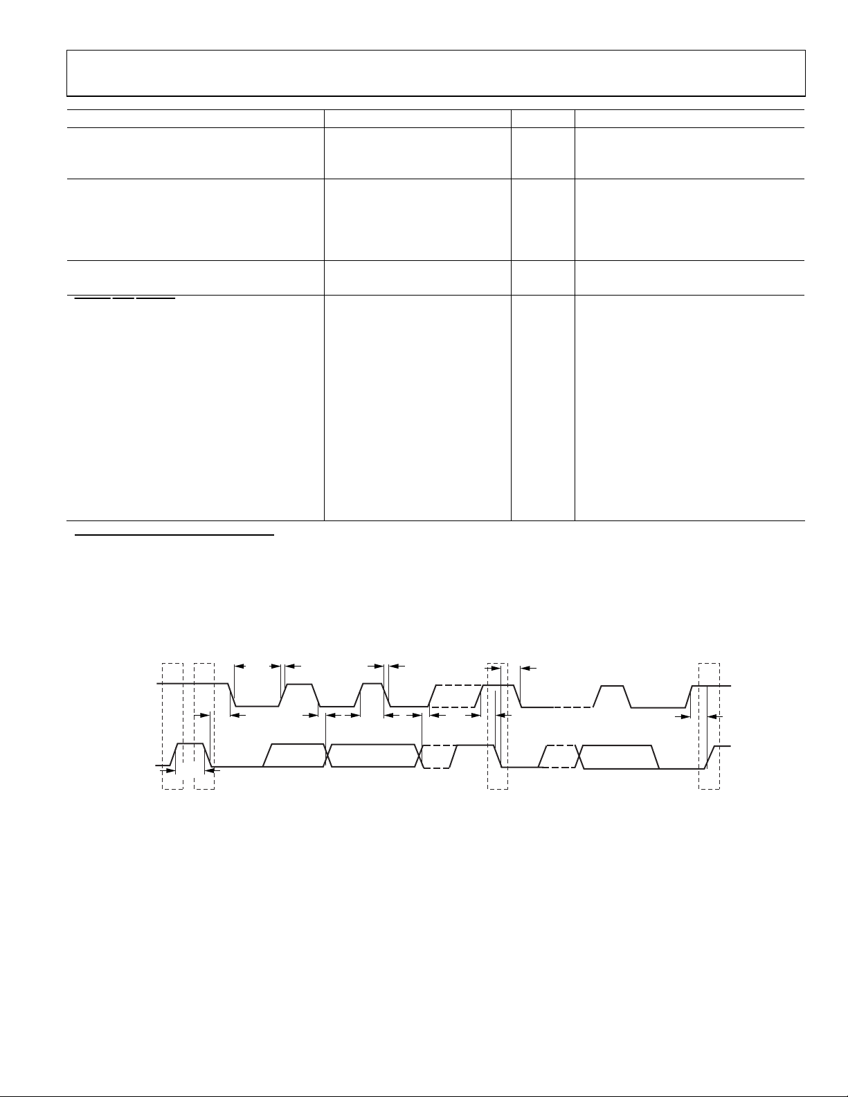
SERIAL BUS TIMING
Clock Frequency, f
Glitch Immunity, t
Bus Free Time, t
Start Setup Time, t
Start Hold Time, t
Stop Condition Setup Time t
SCL Low Time, t
SCL High Time, t
SCL, SDA Rise Time, t
SCL, SDA Fall Time, t
Data Setup Time, t
Detect Clock Low Timeout, t
1
Typicals are at TA = 25°C and represent most likely parametric norm. Standby current typ is measured with VCC = 3.3 V. Timing specifications are tested at logic levels of
= 0.8 V for a falling edge and VIH = 2.1 V for a rising edge.
V
IL
2
Operation at 5.5 V is guaranteed by design, not production tested.
3
Recommend use of 100 kΩ pull-up resistors for all open-drain outputs from the ADM1034.
4
Guaranteed by design, not production tested.
5
SMBus timeout disabled by default. See the section for more information. SMBUS
V
400 kHz See Figure 2
ns See Figure 2
µs See Figure 2
µs See Figure 2
µs See Figure 2
µs See Figure 2
µs See Figure 2
µs See Figure 2
1000 ns See Figure 2
300 ns See Figure 2
ns See Figure 2
35 ms See Note 5
SCL
SD
t
t
BUF
PS
HD:STA
t
LOW
t
R
t
HD:DAT
t
HIGH
t
F
t
SU:DAT
t
HD:STA
t
SU:STA
S
t
SU:STO
P
04918-0-002
Figure 2. Serial Bus Timing Diagram
Rev. 0 | Page 5 of 40
Page 6

ADM1034
ABSOLUTE MAXIMUM RATINGS
Table 2.
Parameter Rating
Positive Supply Voltage (VCC)
Voltage on Any Input or Output Pin except
FA N_ FAU LT and LOCATION
Voltage on FA N_ FAU LT
Voltage on LOCATION VCC + 0.3 V
Input Current at Any Pin ±20 mA
Maximum Junction Temperature (TJ max) 150°C
Storage Temperature Range
Lead Temperature, Soldering (10 s) 300°C
IR Reflow Peak Temperature 220°C
ESD Rating—All Pins 1500 V
1
−0.3 V to +6.5 V
−0.3 V to +6.5 V
V
CC
−65°C to +150°C
1
During power-up the voltage on
FAN _ FAU LT
should not be higher than VCC.
ESD CAUTION
ESD (electrostatic discharge) sensitive device. Electrostatic charges as high as 4000 V readily accumulate on
the human body and test equipment and can discharge without detection. Although this product features
proprietary ESD protection circuitry, permanent damage may occur on devices subjected to high energy
electrostatic discharges. Therefore, proper ESD precautions are recommended to avoid performance
degradation or loss of functionality.
Stresses above those listed under Absolute Maximum Ratings
may cause permanent damage to the device. This is a stress
rating only; functional operation of the device at these or any
other conditions above those indicated in the operational
section of this specification is not implied. Exposure to Absolute
Maximum Rating conditions for extended periods may affect
device reliability.
THERMAL CHARACTERISTICS
16-Lead QSOP Package:
= 150°C/W, θJC = 39°C/W
θ
JA
Rev. 0 | Page 6 of 40
Page 7

ADM1034
PIN CONFIGURATION AND FUNCTION DESCRIPTIONS
1
DRIVE1
2
TACH1
3
DRIVE2
TACH2
GND
V
CC
THERM
FAN_FAULT/REF D1–
ADM1034
TOP VIEW
4
(Not to Scale)
5
6
7
8
16
SCL
15
SDA
14
ALERT
13
LOCATION
12
D2+
11
D2–
10
D1+
9
04918-0-003
Figure 3. Pin Configuration
Table 3. Pin Function Descriptions
Pin No. Mnemonic Description
1 DRIVE1 DRIVE1 Pin Drives Fan 1. Open-drain output. Requires a pull-up resistor.
2 TACH1 Fan 1 Fan Speed Measurement Input. Connects to the fan’s TACH output to measure the fan speed.
3 DRIVE2 DRIVE2 Pin Drives Fan 2. Open-drain output. Requires a pull-up resistor.
4 TACH2 Fan 2 Fan Speed Measurement Input. Connects to the fan’s TACH output to measure the fan speed.
5 GND Ground for Analog and Digital Circuitry.
6 V
7
8
CC
THERM Can be configured as an overtemperature interrupt output, or as an input (to monitor PROCHOT output of
FA N_ FAU LT/REF FA N_ FAU LT: Open-Drain Output. Asserted low when one or both fans stall. Requires a pull-up resistor to V
Power. Can be powered by 3.3 V standby power if monitoring in low power states is required.
an INTEL CPU). A timer measures assertion times on the
REF: Analog Input Reference for the
THERM Input.
THERM pin (either input or output).
9 D1− Cathode Connection for the First Thermal Diode or Diode-Connected Transistor.
10 D1+ Anode Connection for the First Thermal Diode or Diode-Connected Transistor.
11 D2− Cathode Connection for the Second Thermal Diode or Diode-Connected Transistor.
12 D2+ Anode Connection for the Second Thermal Diode or Diode-Connected Transistor.
13 LOCATION 8-Level Analog Input. Used to determine the correct SMBus version and the SMBus address (in
fixed-and-discoverable mode) and to set the LLL bits in the UDID (in ARP-capable mode).
14
ALERT Open-Drain Output. SMBusALERT pin. Alerts the system in the case of out-of-limit events, such as over
temperature. Can be configured as sticky SMBus mode or comparator mode.
15 SDA
Serial Bus Bidirectional Data. Connects to the SMBus master’s data line. Requires pull-up resistor if not
provided elsewhere in the system.
16 SCL
Serial SMBus Clock Input. Connects to the SMBus master’s clock line. Requires pull-up resistor if not already
provided in the system.
.
CC
Rev. 0 | Page 7 of 40
Page 8
ADM1034
TYPICAL PERFORMANCE CHARACTERISTICS
40
20
0
–20
–40
–60
TEMPERATURE ERROR (°C)
–80
D+ TO GND
D+ TO V
CC
20
15
10
5
0
TEMPERATURE ERROR (°C)
–5
EXT 100mVpp
EXT 250mVpp
–100
0 10203040 5060708090100
LEAKAGE RESISTANCE (MΩ)
Figure 4. Temperature Error vs. PCB Track Resistance DXP to GND and V
0
–10
–20
–30
–40
–50
–60
TEMPERATURE ERROR (°C)
–70
–80
0426810
DEV 32 (°C)
CAPACITANCE (nF)
DEV 33 (°C)
DEV 31 (°C)
12
Figure 5. Remote Temperature Error vs. D+, D− Capacitance
100
90
80
70
60
50
40
30
20
TEMPERATURE ERROR (°C)
10
0
–10
12 3 4 65
SERIES RESISTANCE IN D+/D– LINES (kΩ)
DEV 33
DEV 31
DEV 32
Figure 6. Remote Temperature Error vs. Series Resistance on D+ and D−
04918-0-004
CC
04918-0-005
04918-0-006
–10
01M2M3M4M 65M
04918-0-007
M
Figure 7. Remote Temperature Error vs. Power Supply Noise Frequency
50
45
40
35
30
25
20
15
TEMPERATURE ERROR (°C)
10
5
00
01M2M 4M3M 5M 6M
NOISE FREQUENCY (Hz)
100mV
20mV
50mV
04918-0-008
Figure 8. Remote Temperature Error vs. Common-Mode Noise Frequency
Coupled on D+ and D−
4.0
3.5
3.0
2.5
2.0
1.5
1.0
TEMPERATURE ERROR (°C)
0.5
0
01M 3M2M 5M4M 6M
NOISE FREQUENCY
20mV
10mV
04918-0-009
Figure 9. Remote Temperature Error vs. Differential Mode Noise Frequency
Coupled on D+ and D−
Rev. 0 | Page 8 of 40
Page 9
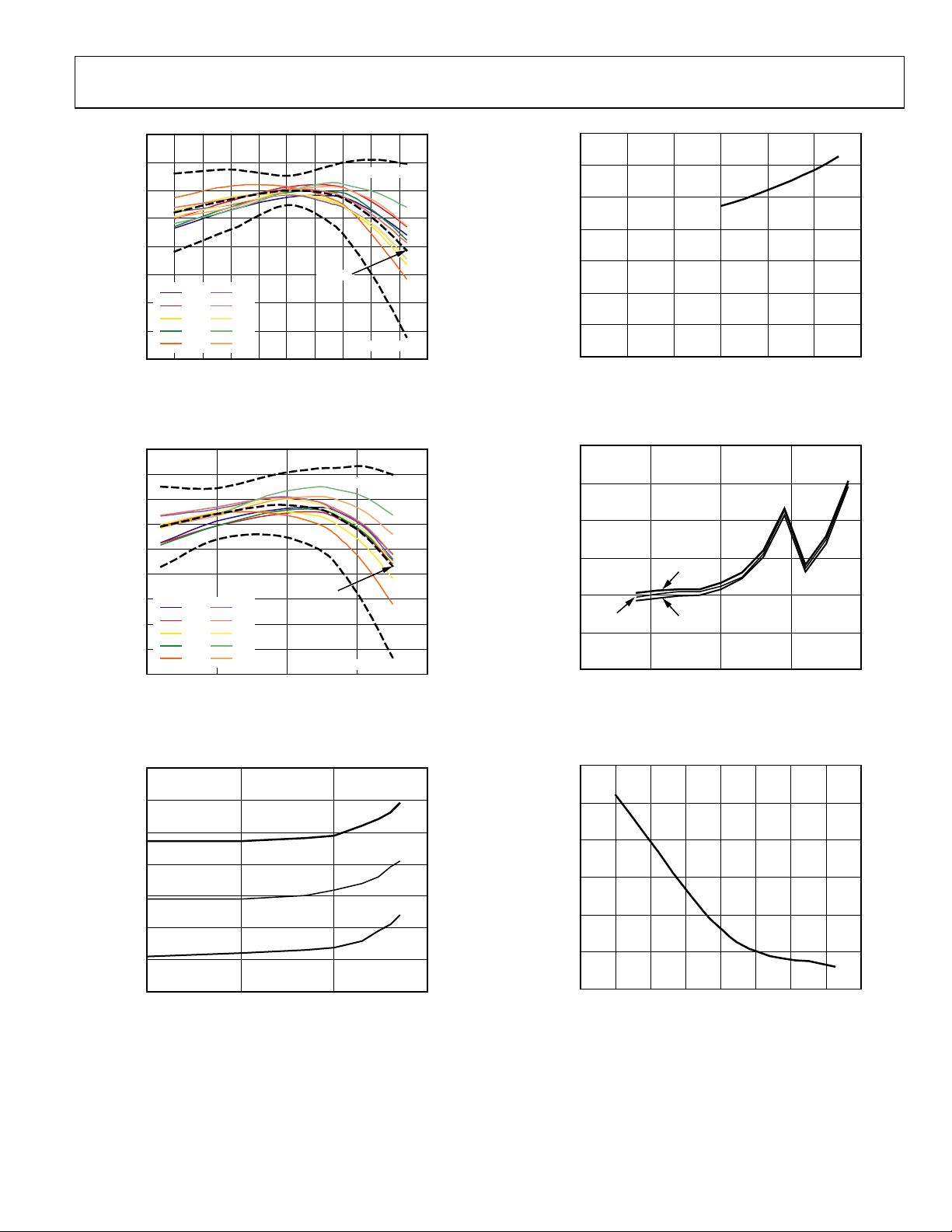
ADM1034
2
1
0
–1
–2
–3
ERROR (°C)
–4
–5
–6
–7
S1
S2
S3
S4
S5
–60 –40 –20 0 80 100 12040 6020 140
V1
V2
V3
V4
V5
TEMPERATURE (
MEAN
°
C)
HIGH 4 SIGMA
LOW 4 SIGMA
Figure 10. Remote Temperature Error vs. Actual Diode Temperature
2
1
0
–1
–2
–3
ERROR (°C)
–4
–5
–6
–7
S1
S2
S3
S4
S5
–50 0 10050 150
V1
V2
V3
V4
V5
TEMPERATURE (°C)
HIGH 4 SIGMA
MEAN
LOW 4 SIGMA
Figure 11. Local Temperature Error vs. Actual Temperature
430
04918-0-010
04918-0-011
0.7
0.6
0.5
0.4
0.3
0.2
STANDBY SUPPLY CURRENT
0.1
0
024531
SUPPLY VOLTAGE (V)
Figure 13. Standby Supply Current vs. Supply Voltage
1200
1000
800
(µA)
600
CC
I
400
DEV 33
200
0
0.01 0.1 1 10010
DEV 31
DEV 32
CONVERSION RATE (Hz)
Figure 14. Supply Current vs. Conversion Rate
1.55
04918-0-013
6
04918-0-014
420
410
400
(µA)
CC
I
390
380
370
360
1 10 1000100
FSCL (kHz)
Figure 12. Standby Supply Current vs. SCLK Frequency
DEV 31
DEV 33
DEV 32
04918-0-012
1.50
1.45
1.40
1.35
SUPPLY CURRENT
1.30
1.25
–60 –40 –20 0 10040 60 8020
TEMPERATURE (°C)
Figure 15. Supply Current vs. ADM1034 Temperature
04918-0-015
Rev. 0 | Page 9 of 40
Page 10
ADM1034
0
0
FUNCTIONAL DESCRIPTION
The ADM1034 is a local- and remote-temperature monitor and
fan controller for use in a variety of applications, including
microprocessor-based systems. The device accurately monitors
remote and ambient temperature and uses that information to
quietly control the speed of a cooling fan. Whenever one of the
fans stalls, the device asserts a
The ADM1034 features a
measures assertions on the
FAN_ FAULT
THERM
THERM
I/O. As an input, this
a low signal to indicate when the measured temperature exceeds
the programmed
THERM
temperature. The ADM1034
communicates over an SMBus 2.0 interface. Its LOCATION
input determines which version of SMBus to use, as well as the
SMBus address (in fixed-and-discoverable mode) and the
LOCATION bits in the UDID (in ARP-capable mode).
INTERNAL REGISTERS
Table 4 gives a brief description of the ADM1034’s principal
internal registers. For more detailed information on the
function of each register, refer to Table 34.
SERIAL BUS INTERFACE
The ADM1034 communicates with the master via the 2-wire
SMBus 2.0 interface. It supports two versions of SMBus 2.0,
determined by the value of the LOCATION input’s resistors.
The first version is fully ARP-capable. This means that it
supports address resolution protocol (ARP), allowing the
master to dynamically address the device on power-up. It
responds to ARP commands such as “Prepare to ARP.”
The second SMBus version, fixed-and-discoverable, is
backwards-compatible with SMBus 1.0 and 1.1. In this mode,
the ADM1034 powers up with a fixed address, which is
determined by the state of the LOCATION pin on power-up.
Note: When using the ADM1034, Addresses 0xC2 and 0xCA
should not be used by any other device on the bus.
LOCATION INPUT
The LOCATION input is a resistor divider input. It has multiple
functions and can specify the SMBus version (in fixed-anddiscoverable or ARP-capable modes); the SMBus address (in
fixed-and-discoverable mode); and the LLL bits (in UDID in
ARP-capable mode).
The voltage of this 8-level input is set by a potential divider. The
voltage on LOCATION is sampled on power-up and digitized
by the on-chip ADC to determine the LOCATION input value.
Because the LOCATION input is sampled only at power-up,
changes made while power is applied have no effect.
output.
pin. As an output, it asserts
V
CC
R1
R2
GND
Figure 16. Bootstrapping the LOCATION Input
PIN 13
ADM1034
LOCATION
04918-0-016
SMBus 2.0 ARP-CAPABLE MODE
In ARP-capable mode, the ADM1034 supports features such as
address resolution protocol (ARP) and unique device identifier
(UDID). The UDID is a 128-bit message that describes the
ADM1034’s capabilities to the master. The UDID also includes a
vendor-specific ID for functionally equivalent devices.
V
CC
LOCATION = 111
LOCATION = 11
LOCATION = 101
LOCATION = 10
ADDRESS = 53h
ADDRESS = 52h
ADDRESS = 51h
ADDRESS = 50h
Figure 17. Setting Up Multiple ADM1034 Addresses in
ARP
1.5kΩ
ARP
1kΩ
ARP
1kΩ
ARP
1kΩ
FD
1kΩ
FD
1kΩ
FD
1.5kΩ
FD
GND
SMBus 2.0 ARP-Capable Mode
In SMBus 2.0 mode, this vendor-specific ID is generated by an
on-chip random number generator. This should enable two
adjacent ADM1034s in the same system to power up with a
different vendor-specific ID, allowing the master to identify the
two separate ADM1034s and assign a different address to each.
The state of the LOCATION input on power-up is also reflected
in the UDID. This is useful when there is more than one
ADM1034 in the system, so the master knows which one it is
communicating with. The complete UDID is listed in Table 6.
The SMBus 2.0 master issues both general and directed ARP
commands. A general command is directed at all ARP devices.
A directed command is targeted at a single device once an
address has been established. The PEC byte must be used for
ARP commands. (Refer to the Packet Error Checking (PEC)
section.) The ADM1034 responds to the following commands:
• Prepare to ARP (general)
• Reset device (general and directed)
• Get UDID (general and directed)
• Assign address (general)
ADM1034 NO. 1
ADM1034 NO. 2
ADM1034 NO. 3
ADM1034 NO. 4
ADM1034 NO. 5
ADM1034 NO. 6
ADM1034 NO. 7
ADM1034 NO. 8
04918-0-017
Rev. 0 | Page 10 of 40
Page 11
ADM1034
Table 4. Internal Register Descriptions
Register Description
Configuration Provides control and configuration of various functions on the device.
Conversion Rate Determines the number of measurements per second completed by the ADM1034.
Address Pointer
Status Provides the status of each limit comparison.
Interrupt Mask
Value and Limit Stores the results of temperature and fan speed measurements, along with their limit values.
Offset
THERM Limit and Hysteresis Contains the temperature value at which THERM is asserted and indicates the level of hysteresis.
Look-Up Table Used to program the look-up table for the fan-speed-to-temperature profile.
THERM % Ontime and
THERM % Limit
Table 5. Resistor Ratios for Setting LOCATION Bits
Ideal Ratio R2/(R1 + R2) R1 kΩ R2 Ω Actual R2/(R1 + R2) Error % SMBus Ver SMBus Address UDID LLL
N/A 0 O/C 1 0 ARP
0.8125 18 82 0.82 +0.75 ARP1 N/A 110
0.6875 22 47 0.6812 −0.63 ARP1 N/A 101
0.5625 12 15 0.5556 −0.69 ARP1 N/A 100
0.4375 15 12 0.4444 +0.69 FD1 0x53 N/A
0.3125 47 22 0.3188 +0.63 FD1 0x52 N/A
0.1875 82 18 0.18 −0.75 FD1 0x51 N/A
N/A O/C 0 0 0 FD1 0x50 N/A
1
FD denotes fixed-and-discoverable mode, ARP denotes ARP-capable mode.
Table 6. UDID Values
Bit No. Name Function Value
<127:120> Device Capabilities
<119:112> Version/Revision UDID version number (Version 1) and silicon revision identification 00001010
<111:96> Vendor ID
<95:80> Device ID Device ID.
<79:64> Interface
<63:48> Subsystem Vendor ID Subsystem Vendor ID = 0 (subsystem fields are unsupported).
<47:32> Subsystem Device ID Subsystem Device ID = 0 (subsystem fields are unsupported).
<31:0> Vendor Specific ID
Contains the address that selects one of the other internal registers. When writing to the ADM1034, the
first byte of data is always a register address, written to the address pointer register.
Allows the option to mask
ALERTs due to particular out-of-limit conditions.
Allows the local and remote temperature channel readings to be offset by a twos complement value
written to them. These values are automatically added to the temperature values (or subtracted from them
if negative). This allows the systems designer to optimize the system if required, by adding or subtracting
up to 15.875°C from a temperature reading.
Reflects the state of the
THERM input and monitors the duration of the assertion time of the signal as a
percentage of a time window. The user can program the length of the time window.
1
Describes the ADM1034’s capabilities (for instance, that it supports PEC and uses a
N/A 111
11000001
random number address device).
Analog Devices vendor ID number, as assigned by the SBS Implementer’s Forum or
the PCI SIG.
00010001
11010100
00010000
00110100
Identifies the protocol layer interfaces supported by the ADM1034. This represents
SMBus 2.0 as the Interface version..
00000000
00000100
00000000
00000000
00000000
00000000
A unique number per device. Contains LOCATION information (LL) and a 16-bit
random number (x). See Table 5 for information on setting the LLL bits.
00000000
00000LLL
xxxxxxxx
xxxxxxxx
Rev. 0 | Page 11 of 40
Page 12

ADM1034
SMBus 2.0 FIXED-AND-DISCOVERABLE MODE
The ADM1034 also supports fixed-and-discoverable mode,
which is backwards-compatible with SMBus 1.0 and 1.1. Fixedand-discoverable mode supports all the same functionality as
ARP-capable mode, except for assign address—in which case it
powers up with a fixed address and is not changed by the assign
address call. The fixed address is determined by the state of the
LOCATION pin on power-up.
SMBus 2.0 READ AND WRITE OPERATIONS
The master initiates data transfer by establishing a start
condition, defined as a high-to-low transition on the serial data
line (SDA) while the serial clock line (SCL) remains high. This
indicates that an address/data stream is to follow. All slave
peripherals connected to the serial bus respond to the start
condition and shift in the next 8 bits, which consist of a 7-bit
address (MSB first) plus an R/
direction of the data transfer (whether data is written to or read
from the slave device).
1. The peripheral that corresponds to the transmitted address
responds by pulling the data line low during the low period
before the 9th clock pulse, which is known as the
acknowledge bit. All other devices on the bus remain idle
while the selected device waits for data to be read from or
written to it. If the R/
slave device. If the R/
2. Data is sent over the serial bus in sequences of 9 clock
pulses—8 bits of data followed by an acknowledge bit from
the slave device. Transitions on the data line must occur
during the low period of the clock signal and remain stable
during the high period, because a low-to-high transition
when the clock is high may be interpreted as a stop signal.
The number of data bytes that can be transmitted over the
serial bus in a single read or write operation is limited only
by what the master and slave devices can handle.
bit. This last bit determines the
W
bit is a 0, the master writes to the
W
bit is a 1, the master reads from it.
W
It is not possible to mix read and write in one operation,
because the type of operation is determined at the beginning
and cannot be changed without starting a new operation.
To write data to one of the device data registers or to read data
from it, the address pointer register (APR) must be set so that
the correct data register is addressed; then data can be written
into that register or read from it. The first byte of a write
operation always contains an address that is stored in the APR.
If data is to be written to the device, then the write operation
contains a second data byte, which is written to the register
selected by the APR.
As illustrated in Figure 18, the device address is sent over the
bus, followed by R/
bytes. The first data byte is the address of the internal data
register to be written to, which is stored in the APR. The second
data byte is the data to be written to the internal data register.
When reading data from a register there are two possibilities.
If the ADM1034’s APR value is unknown or incorrect, it must
be set to the correct value before data can be read from the
desired data register. To do this, perform a write to the ADM1034
as before, but send only the data byte containing the register.
(See Figure 19.) A read operation is then performed, using the
serial bus address and the R/
byte read from the data register. (See Figure 20.)
However, if the APR is already at the desired address, data can
be read from the corresponding data register without first
writing to the APR. In this case, Figure 19 can be omitted.
In Figure 18 to Figure 20, the serial bus address is determined
by the state of the LOCATION pin on power-up.
set to 0. This is followed by two data
W
bit set to 1, followed by the data
W
3. When all data bytes have been read or written, stop
conditions are established. In write mode, the master pulls
the data line high during the 10th clock pulse to assert a
stop condition. In read mode, the master device overrides
the acknowledge bit by pulling the data line high during
the low period before the 9th clock pulse. This is known as
no acknowledge. The master takes the data line low during
the low period before the 10th clock pulse, then high
during the 10th clock pulse to assert a stop condition.
Rev. 0 | Page 12 of 40
Page 13

ADM1034
S
SCL
SDA
START BY
MASTER
119
A6
A5 A4 A3 A2 A1 A0 R/W D7
ACK. BY
FRAME 1
SERIAL BUS ADDRESS BYTE
SCL (CONTINUED)
SDA (CONTINUED)
ADM1034
D6 D5 D4 D3 D2 D1 D0
ADDRESS POINTER REGISTER BYTE
D7 D6 D5 D4 D3
FRAME 3
DATA BYTE
FRAME 2
D2
D1 D0
91
ACK. BY
ADM1034
9
ACK. BY
ADM1034
STOP BY
MASTER
04918-0-021
Figure 18. Writing a Register Address to the Address Pointer Register, then Writing Data to the Selected Register
SCL
SDA
START BY
MASTER
119
A6 A5 A4 A3 A2 A1 A0 R/W D7
ACK. BY
FRAME 1
SERIAL BUS ADDRESS BYTE
ADM1034
Figure 19. Writing to the Address Pointer Register Only (Send Byte)
D6 D5 D4 D3 D2 D1 D0
ADDRESS POINTER REGISTER BYTE
FRAME 2
9
ACK. BY
ADM1034
STOP BY
MASTER
04918-0-022
119 9
SCL
DA
START BY
MASTER
A6 A5 A4 A3 A2 A1 A0 D7 D6 D5 D4 D3 D2 D1 D0
FRAME 1
SERIAL BUS ADDRESS BYTE
R/W
ADM1034
ACK. BY
FRAME 2
DATA BYTE FROM ADM1034
NO ACK. BY
ADM1034
STOP BY
MASTER
04918-0-023
Figure 20. Reading Data from a Previously Selected Register
Rev. 0 | Page 13 of 40
Page 14

ADM1034
REGISTER ADDRESSES FOR SINGLE/BLOCK BYTE MODES
The ADM1034 supports single-byte as well as block read and
write operations. The register address determines whether a
single-byte or multiple-byte (block) operation is run. For a
single-byte operation, the MSB of the register address is set to 0;
for a multiple-byte operation, it is set to 1. The number of bytes
read in a multiple-byte operation is set in the #Bytes/Block Read
Register at Address 0x00. The number of bytes written to the
ADM1034 is specified during the block-write operation. The
addresses quoted in the register map and throughout this data
sheet assume single-byte operation. For multiple-byte
operations, set the MSB of each register address to 1.
WRITE OPERATIONS
The SMBus specifications define protocols for read and write
operations. The ADM1034 supports send-byte, write-byte, and
block-byte SMBus write protocols. The following abbreviations
are used in the diagrams:
S—START
P—STOP
R—REA D
W—W RI TE
A—AC KNOWLE DGE
—NO ACKNOWLEDGE
A
Send Byte
In this operation, the master device sends a single-command
byte to a slave device as follows:
1. The master device asserts a start condition on SDA.
2. The master sends a 7-bit address followed by the write bit
(low).
3. The addressed slave device asserts ACK on SDA.
4. The master sends the register address.
5. The slave asserts ACK on SDA.
6. The master asserts a stop condition on SDA, and the
transaction ends.
W
A
ADDRESS
REG
P
A
04918-0-018
SLAVE
S
ADDRESS
Figure 21. Send Byte
The ADM1034 uses the send-byte operation to write a register
address to the APR for a subsequent read from the same
address. (See Figure 24.) The user may be required to read data
from the register immediately after setting up the address. If so,
the master can assert a repeat start condition immediately after
the final ACK and carry out a single-byte read without asserting
an intermediate stop condition.
Write Byte
In this operation, the master device sends a register address and
one data byte to the slave device as follows:
1. The master asserts a start condition on SDA.
2. The master sends the 7-bit slave address followed by a
write bit (low).
3. The addressed slave device asserts ACK on SDA.
4. The master sends the register address. The MSB of the
register address should equal 0 for a write-byte operation.
If the MSB equals 1, a block-write operation takes place.
5. The slave asserts ACK on SDA.
6. The master sends a data byte.
7. The slave asserts ACK on SDA.
8. The master asserts a stop condition on SDA to end the
transaction.
SLAVE
S
ADDRESS
Figure 22. Write Byte Operation
W
A
ADDRESS
REG
DATA
A
A
P
04918-0-019
Block Write
In this operation, the master device writes a block of data to a
slave address as follows. A maximum of 32 bytes can be written.
1. The master asserts a start condition on SDA.
2. The master sends the 7-bit slave address followed by a
write bit (low).
3. The addressed slave device asserts ACK on SDA.
4. The master sends the register address. The register address
sets up the address pointer register and determines
whether a block-write (MSB = 1) or a byte-write (MSB = 0)
takes place.
5. The slave asserts ACK on SDA.
6. The master sends the byte count.
7. The slave asserts ACK on SDA.
8. The master sends N data bytes.
9. The slave asserts ACK on SDA after each byte.
10. The master asserts a stop condition on SDA to end the
transaction.
S
ADDRESS
SLAVE
REGISTER
W
A
ADDRESS
Figure 23. Block Write to RAM
A
BYTE
COUNT
A
DATA 1
A DATA N
DATA 2
A
A
P
04918-0-020
Rev. 0 | Page 14 of 40
Page 15

ADM1034
(
READ OPERATIONS
Receive Byte
This is useful when repeatedly reading a single register. The
register address must be set up prior to this, with the MSB at 0
to read a single byte. In this operation, the master device
receives a single byte from a slave device as follows:
1. The master device asserts a start condition on SDA.
2. The master sends the 7-bit slave address followed by the
read bit (high).
3. The addressed slave device asserts ACK on SDA.
4. The master receives a data byte.
5. The master sends NO ACK on SDA.
6. The master asserts a stop condition on SDA, and the
transaction ends.
In the ADM1034, the receive-byte protocol is used to read a
single byte from a register whose address has previously been
set by a send-byte or write-byte operation.
S
ADDRESS
SLAVE
REGISTER
W
A
ADDRESS
Figure 25. Block Read from RAM
SLAVE
A
S
ADDRESS
SMBus TIMEOUT
The ADM1034 has a programmable SMBus timeout feature.
When this is enabled, the SMBus typically times out after 25 ms
of no activity. The timeout is disabled by default. It prevents
hangups by releasing the bus after a period of inactivity.
To enable the SDA timeout, set the SDA timeout bit (Bit 5) of
Configuration Register 1 (Address 0x01) to 1.
To enable the SCL timeout, set the SCL timeout bit (Bit 4) of
Configuration Register 1 (Address 0x01) to 1.
PACKET ERROR CHECKING (PEC)
The ADM1034 also supports packet error checking (PEC). This
optional feature is triggered by the extra clock for the PEC byte.
The PEC byte is calculated using CRC-8. The frame check
sequence (FCS) conforms to CRC-8 by the following:
BYTE
DATA 1
A
R
A
COUNT
A DATA N
P
A
04918-0-025
SLAVE
S
ADDRESS
Figure 24. Receive Byte
A
R
DATA
P
A
04918-0-024
Block Read
In this operation, the master reads a block of data from a slave
device. The number of bytes to be read must be set in advance.
To d o th is , u se a write-byte operation to the #Bytes/Block Read
Register at Address 0x00. The register address determines
whether a block-read or a read-byte operation is to be completed
(set MSB to 1 to specify a block-read operation). A maximum of
32 bytes can be read.
1. The master asserts a start condition on SDA.
2. The master sends the 7-bit slave address followed by the
write bit (low).
3. The addressed slave device asserts ACK on SDA.
4. The master sends the register address (MSB = 1).
5. The slave asserts ACK on SDA.
6. The master asserts a repeated start on SDA.
7. The master sends the 7-bit slave address followed by the
read bit (high).
8. The slave asserts ACK on SDA.
9. The slave sends the byte count.
10. The master asserts ACK on SDA.
11. The slave sends N data bytes.
12. The master asserts ACK on SDA after each data byte.
13. The master does not acknowledge after the Nth data byte.
14. The master asserts a stop condition on SDA to end the
transaction.
)
For more information, consult
128+++= xxxxC
www.SMBus.org.
ALERT RESPONSE ADDRESS (ARA)
ALERT RESPONSE
S
ADDRESS
Figure 26. ALERT Response Address
When multiple devices exist on the same bus, the ARA feature
allows an interrupting device to identify itself to the host.
The
SMBusALERT
to a common
If a device’s
1.
output can be used as an interrupt output or as an
ALERT
. One or more
SMBusALERT
ALERT
SMBusALERT
line goes low, the following occurs:
is pulled low.
line, connected to the master.
2. The master initiates a receive-byte operation and sends the
alert response address (ARA 0001 100). This is a general
call address that must not be used as a specific address.
3. The device with the low
ARA, and the master reads its device address. Once the
address is known, it can be interrogated in the usual way.
4. If low
output is detected in more than one device,
ALERT
the one with the lowest device address has priority, in
accordance with normal SMBus arbitration.
5. Once the ADM1034 has responded to the ARA, it resets its
output. However, if the error persists, the
ALERT
re-asserted on the next monitoring cycle.
DEVICE
R
A
ADDRESS
outputs can be connected
ALERT
output responds to the
ALERT
A
P
04918-0-043
ALERT
is
Rev. 0 | Page 15 of 40
Page 16

ADM1034
TEMPERATURE MEASUREMENT SYSTEM
INTERNAL TEMPERATURE MEASUREMENT
The ADM1034 contains an on-chip band gap temperature
sensor. The on-chip ADC performs conversions on the sensor’s
output, outputting the data in 13-bit format. The resolution of
the local temperature sensor is 0.03125°C.
Table 7 shows the format of the temperature data MSBs. Table 8
shows the same for the LSBs. To ensure accurate readings, read
the LSBs first. This locks the current LSBs and MSBs until the
MSBs are read. They then start to update again. (Reading only
the MSBs does not lock the registers.) Temperature updates to
the look-up table take place in parallel; so fan speeds may be
updated even if the MSBs are locked.
Table 7. Temperature Data Format
(Local Temperature and Remote Temperature High Bytes)
Temperature (°C) Digital Output
−64°C
−40°C
−32°C
−2°C
−1°C
0°C 0100 0000
1°C 0100 0001
2°C 0100 0010
10°C 0100 1010
20°C 0101 0100
50°C 0111 0010
75°C 1000 1011
100°C 1010 0100
125°C 1011 1101
150°C 1101 0110
191°C 1111 1111
0000 0000
0001 1000
0010 0000
0011 1110
0011 1111
Table 8. Local and Remote Sensor Extended Resolution
Extended Resolution (°C) Temperature Low Bits
0.0000 00000
0.03125 00001
0.0625 00010
0.125 00100
0.250 01000
0.375 01100
0.500 10000
0.625 10100
0.750 11000
0.875 11100
REMOTE TEMPERATURE MEASUREMENT
The ADM1034 can measure the temperature of two external
diode sensors or diode-connected transistors, which are
connected to Pins 9 and 10 and Pins 11 and 12. These pins are
dedicated temperature input channels. The series resistance
cancellation (SRC) feature can automatically cancel out the
effect of up to 1 kΩ of resistance in series with the remote
thermal diode.
The forward voltage of a diode or diode-connected transistor,
operated at a constant current, exhibits a negative temperature
coefficient of about −2 mV/°C. Unfortunately, the absolute
value of V
calibration is required to null this out. Therefore, the technique
is unsuitable for mass production.
Te mp e ra t ur e (°C) = (MSB − 64°C) + (LSB × 0.03125)
Example: MSB = 0101 0100 = 84d
LSB = 11100 = 28
Temperature °C = (84 – 64) + (28 × 0.03125) = 20.875
varies from device to device, and individual
be
ADM1034
D+
2N3906
D–
Figure 27. Measuring Temperature by Using Discreet Transistors
Rev. 0 | Page 16 of 40
2N3904
ADM1034
D+
D–
04918-0-026
Page 17

ADM1034
T
The ADM1034 operates at three different currents to measure
the change in V
. Figure 28 shows the input signal conditioning
be
used to measure the output of an external temperature sensor. It
also shows the external sensor as a substrate transistor, provided
for temperature monitoring on some microprocessors. The
external sensor could work equally well as a discrete transistor.
If a discrete transistor is used, the collector is not grounded, and
should be linked to the base. If a PNP transistor is used, the base
is connected to the D− input and the emitter to the D+ input. If
an NPN transistor is used, the emitter is connected to the D−
input and the base to the D+ input.
If the sensor is used in a very noisy environment, a capacitor
value up to 1000 pF may be placed between the D+ and D−
inputs to filter the noise. However, additional parasitic
capacitance on the lines between D+, D−, and the thermal diode
should also be considered. The total capacitance should never
be greater than 1000 pF.
To m e as ur e ea ch ∆ V
, the sensor is switched between operating
be
currents of I, (N1 × I), and (N2 × I). The resulting waveform is
passed through a 65 kHz low-pass filter to remove noise, then to
a chopper-stabilized amplifier that amplifies and rectifies the
waveform. This produces a dc voltage proportional to ∆V
.
be
These voltage measurements determine the temperature of the
thermal diode, while automatically compensating for any series
resistance on the D+ and/or D− lines. The temperature is stored
in two registers as a 13-bit word.
To further reduce the effects of noise, digital filtering is
performed by averaging the results of 16 measurement cycles at
conversion rates of less than or equal to 8 Hz. An external
temperature measurement takes nominally 32 ms when
averaging is enabled and 6 ms when averaging is disabled.
One LSB of the ADC corresponds to 0.03125°C. The ADM1034
can theoretically measure temperatures from −64°C to
+191.96875°C, although these are outside its operating range.
The extended temperature resolution data format is shown in
Table 8. The data for the local and remote channels is stored in
the extended temperature resolution registers (Reg. 0x40 =
Local, Reg. 0x42 = Remote 1, and Reg. 0x44 = Remote 2).
Table 9.Temperature Measurement Registers
Register Description Default
0x40 Local Temperature, LSBs 0x00
0x41 Local Temperature, MSBs 0x00
0x42 Remote 1 Temperature, LSBs 0x00
0x43 Remote 1 Temperature, MSBs 0x00
0x44 Remote 2 Temperature, LSBs 0x00
0x45 Remote 2 Temperature, MSBs 0x00
High and low temperature limit registers are associated with
each temperature measurement channel. Exceeding the
programmed high and low limits sets the appropriate status bit.
Exceeding either limit can cause an
SMBusALERT
interrupt.
Table 10. Temperature Measurement Limit Registers
Register Description Default
0x0B Local High Limit 0x8B (75°C)
0x0C Local Low Limit 0x54 (20°C)
0x0D
Local
THERM Limit
0x95 (85°C)
0x0E Remote 1 High Limit 0x8B (75°C)
0x0F Remote 1 Low Limit 0x54 (20°C)
0x10
Remote 1
THERM Limit
0x95 (85°C)
0x11 Remote 2 High Limit 0x8B (75°C)
0x12 Remote 2 Low Limit 0x54 (20°C)
0x13
Remote 2
THERM Limit
0x95 (85°C)
V
f
= 65kHz
C
DD
V
OUT+
TO ADC
V
OUT–
04918-0-027
REMOTE
SENSING
RANSISTOR
IN1× I
D+
D–
N2 × I
Figure 28. ADM1034 Signal Conditioning
I
BIAS
LOW-PASS FILTER
Rev. 0 | Page 17 of 40
Page 18

ADM1034
ADDITIONAL FUNCTIONS
Several other temperature measurement functions available on
the ADM1034 offer the systems designer added flexibility.
Turn-off Averaging
The ADM1034 performs averaging at conversion rates of less
than or equal to 8 conversions per second. This means that the
value in the measurement register is the average of 16 measurements. For faster measurements, set the conversion rate to 16
conversions per second or greater. (Averaging is not carried out
at these conversion rates.) Alternatively, switch off averaging at
the slower conversion rates by setting Bit 1 (AVG) of
Configuration 1 Register (Address 0x01).
Single-Channel ADC Conversions
In normal operating mode, the ADM1034 converts on three
temperature channels: the local temperature channel, and the
remote 1 and remote 2 channels. However, the user has the
option to set up the ADM1034 to convert on one channel only.
To enable single-channel mode, the user sets the round-robin
bit (Bit 7) in Configuration Register 2 (Address 0x02) to 0.
When the round-robin bit equals 1, the ADM1034 converts on
all three temperature channels. In single-channel mode, it
converts on one channel only, to be determined by the state of
the channel selector bits (Bits 5 and 4) of the Configuration
Register 2 (Address 0x02).
Table 11. Channel Selector
Bits 5:4 Channel Selector (Configuration 2)
00 Local Channel = Default
01 Remote 1 Channel
10 Remote 2 Channel
11 Reserved
Removing Temperature Errors
As CPUs run faster and faster, it gets more difficult to avoid
high frequency clocks when routing the D+ and D− traces
around a system board. Even when the recommended layout
guidelines are followed, temperature errors attributed to noise
coupled onto the D+ and D− lines remain. High frequency
noise generally gives temperature measurements that are
consistently too high. The ADM1034 has Local, Remote 1, and
Remote 2 temperature offset registers at 0x16, 0x17, and 0x18—
one for each channel. By completing a one-time calibration, the
user can determine the offset caused by the system board noise
and remove it using the offset registers. The registers
automatically add a twos compliment word to the remote
temperature measurements, ensuring correct readings in the
value registers.
Table 12. Offset Registers
Registration Description Default
0x16 Local Offset 0x00
0x17 Remote 1 Offset 0x00
0x18 Remote 2 Offset 0x00
Table 13. Offset Register Values
Code Offset Value
0 0000 000 0°C (Default Value)
0 0000 001 0.125°C
0 0000 111 0.875°C
0 0001 111 1.875°C
0 0111 111 7.875°C
0 1111 111 15.875°C
1 0000 000
1 1111 000
−16°C
−0.875°C
Rev. 0 | Page 18 of 40
Page 19

ADM1034
T
LAYOUT CONSIDERATIONS
Digital boards can be electrically noisy environments. Try
to protect the analog inputs from noise, particularly when
measuring the very small voltages from a remote diode sensor.
Take the following precautions:
• Place the ADM1034 as close as possible to the remote
sensing diode. A distance of 4 inches to 8 inches is
adequate, provided that the worst noise sources such
as clock generators, data/address buses, and CRTs are
avoided.
• Route the D+ and D− tracks close together, in parallel, with
grounded guard tracks on each side. Provide a ground
plane under the tracks if possible.
• Use wide tracks to minimize inductance and reduce noise
pickup. At least 5 mil track width and spacing are
recommended.
GND
D+
D–
GND
Figure 29. Arrangement of Signal Tracks
5MIL
5MIL
5MIL
5MIL
5MIL
5MIL
5MIL
04918-0-028
• Try to minimize the number of copper/solder joints,
because they can cause thermocouple effects. Where
copper/solder joints are used, make sure that they are in
both the D+ and D− paths and at the same temperature.
Thermocouple effects are not a major problem because
1°C corresponds to approximately 200 µV, and thermocouple voltages are approximately 3 µV/°C of temperature
difference. Unless there are two thermocouples with a big
temperature differential between them, the voltages should
be much less than 200 µV.
• Place a 0.1 µF bypass capacitor close to the ADM1034.
• If the distance to the remote sensor is more than 8 inches,
twisted pair cable is recommended. This works up to about
6 feet to 12 feet.
• For very long distances (up to 100 feet), use shielded
twisted pair such as Belden #8451 microphone cable.
Connect the twisted pair to D+ and D− and the shield to
GND, close to the ADM1034. Leave the remote end of the
shield unconnected to avoid ground loops.
Because the measurement technique uses switched current
sources, excessive cable and/or filter capacitance can affect the
measurement. When using long cables, the filter capacitor C1
may be reduced or removed. In any case, the total shunt
capacitance should never exceed 1000 pF.
Noise Filtering
For temperature sensors operating in noisy environments,
common practice is to place a capacitor across the D+ and D−
pins to help combat the effects of noise. However, large
capacitances affect the accuracy of the temperature measurement,
leading to a recommended maximum capacitor value of 1000 pF.
While this capacitor reduces the noise, it does not eliminate it,
making it difficult to use the sensor in a very noisy environment.
The ADM1034 has a major advantage over other devices when
it comes to eliminating the effects of noise on the external
sensor. The series resistance cancellation feature allows a filter
to be constructed between the external temperature sensor and
the part. The effect of any filter resistance seen in series with the
remote sensor is automatically cancelled from the temperature.
The construction of a filter allows the ADM1034 and the
remote temperature sensor to operate in noisy environments.
Figure 30 shows a low-pass R-C-R filter with the following
values: R = 100 Ω and C = 1 nF. This filtering reduces both
common-mode noise and differential noise.
100Ω
REMOTE
EMPERATURE
SENSOR
Figure 30. Filter between R emote Sensor and ADM1034
100Ω
1nF
D+
D–
04110-0-009
Rev. 0 | Page 19 of 40
Page 20

ADM1034
LIMITS, STATUS REGISTERS, AND INTERRUPTS
High and low limits are associated with each measurement
channel on the ADM1034. These can form the basis of system
status monitoring. A status bit can be set for any out-of-limit
condition and detected by polling the device. Alternatively,
SMBusALERT
microcontroller of an out-of-limit condition.
8-BIT LIMITS
The following is a list of all the 8-bit limits on the ADM1034:
Table 14. Temperature Limit Registers
Register Description Default
0x0B Local High Limit 0x8B (75°C)
0x0C Local Low Limit 0x54 (20°C)
0x0D
0x0E Remote 1 High Limit 0x8B (75°C)
0x0F Remote 1 Low Limit 0x54 (20°C)
0x10
0x11 Remote 2 High Limit 0x8B (75°C)
0x12 Remote 2 Low Limit 0x54 (20°C)
0x13
Table 15.
Register Description Default
0x19
OUT-OF-LIMIT COMPARISONS
The ADM1034 measures all parameters in a round-robin
format and sets the appropriate status bit for out-of limit
conditions. Comparisons are made differently, depending on
whether the measured value is compared to a high or low limit.
High Limit: ≥ Comparison Performed
s can be generated to flag a processor or
Local
Remote 1
Remote 2
THERM
THERM % Limit
THERM Limit
THERM Limit
THERM Limit
Limit Register
0x95 (85°C)
0x95 (85°C)
0x95 (85°C)
0xFF default
The ADC performs round-robin conversions and takes 11 ms
for the local temperature measurement and 32 ms for each
remote temperature measurement with averaging enabled.
The total monitoring cycle time for the average temperatures is
therefore nominally
(2 × 32) + 11 = 75 ms
Once the conversion time elapses, the round robin starts again.
For more information, refer to the Conversion Rate Register
section.
Fan TACH measurements take place in parallel and are not
synchronized with the temperature measurements in any way.
STATUS REGISTERS
The results of limit comparisons are stored in the status
registers. A 1 represents an out-of-limit measurement; a
0 represents an in-limit measurement. The status registers are
located at Addresses 0x4F to 0x51.
If the measurement is outside its limits, the corresponding
status register bit is set to 1. It remains set at 1 until the
measurement falls back within its limits and it is read or until
an ARA is completed.
Poll the state of the various measurements by reading the status
registers over the serial bus. If Bit 0 (
Register 3 (Address 0x51) is set, this means that the
output has been pulled low by the ADM1034.
Pin 14 can be configured as a
automatically notifies the system supervisor of an out-of-limit
condition. Reading the status register clears the status bit as long
as the error condition is gone.
SMBusALERT
ALERT
low) of Status
ALERT
output. This
Low Limit: < Comparison Performed
ANALOG MONITORING CYCLE TIME
The analog monitoring cycle time begins on power-up, or, if
monitoring has been disabled, by writing a 1 to the monitor/
STBY bit of Configuration Register 1, (Address 0x01). The ADC
measures each one of the analog inputs in turn; as each
measurement is completed, the result is automatically stored in
the appropriate value register. The round-robin monitoring
cycle continues unless it is disabled by writing a 0 to the
monitor/STBY bit (Bit 0) of Configuration Register 1
(Address 0x01).
Rev. 0 | Page 20 of 40
Status register bits are sticky. Whenever a status bit is set due to
an out-of-limit condition, it remains set—even after the
triggering event has gone. The only way to clear the status bit is
to read the status register (after the event has gone). Interrupt
mask registers (Reg. 0x08, Reg. 0x09, Reg. 0x0A) allow
individual interrupt sources to be masked from causing an
. However, if one of these masked interrupt sources goes
ALERT
out of limit, its associated status bit is set in the status register.
Page 21

ADM1034
A
Table 16. Interrupt Status Register 1 (Reg. 0x4F)
Bit No. Name Description
7 LH
6 LL
5 R1H
4 R1L
3 R1D
2 R2H
1 R2L
0 R2D
1 = Local high temperature limit has been
exceeded.
1 = Local low temperature limit has been
exceeded.
1 = Remote 1 high temperature limit has
been exceeded.
1 = Remote 1 low temperature limit has
been exceeded.
1 = Remote 1 diode error; indicates an open
or short on the D1+/D1− pins.
1 = Remote 2 high temperature limit has
been exceeded.
1 = Remote 2 low temperature limit has
been exceeded.
1 = Remote 2 diode error; indicates an open
or short on the D2+/D2− pins.
Table 17. Status Register 2 (Reg. 0x50)
Bit No. Name Description
7 LT
6 R1T
5 R2T
4 T%
3 TA
2 TS
1 Res Reserved.
0 Res Reserved.
1 = Local
been exceeded.
1 = Remote 1
been exceeded.
1 = Remote 2
been exceeded.
1 =
exceeded.
1 = One of the
exceeded; and the
has been asserted.
1 =
active; clears on a read if
active. Does not generate an
ALERT comp mode.
THERM temperature limit has
THERM temperature limit has
THERM temperature limit has
THERM % ontime limit has been
THERM limits has been
THERM output signal
THERM state. Indicates the THERM pin is
THERM is not
ALERT in
Table 18. Status Register 3 (Reg. 0x51)
Bit No. Name Description
7 F1S 1 = Fan 1 has stalled.
6 FA
5 F2S 1 = Fan 2 has stalled.
4 Res Reserved.
3 Res Reserved.
2 Res Reserved.
1 Res Reserved.
0
ALERT 1 = ALERT low; indicates the ALERT line has
1 = Fan alarm speed. Fan1 and Fan 2 are
running at alarm speed.
been pulled low.
ALERT
The ADM1034 generates an
measurement is made (if it is not masked out). The user can
also detect out-of-limit conditions by polling the ADM1034
status registers. It is important to note how the SMBus
output behaves when writing interrupt handler software.
The
operate in either
In
the measurement falls back within its programmed limits and
either the status register is read or an ARA is completed. In
comp mode, the
temperature measurement falls back within the programmed
limits.
Configuring the
For
(Bit 3) of the Configuration Register 1 (Address 0x01) to 0.
In
goes outside of its programmed limit. If the corresponding
mask bit is not set, the
measured value falls back within the limits, the
remains low until the corresponding status register is read or
until an ARA is completed (as long as no other measurement is
outside its limits).
For comp mode, set the
Configuration Register 1 (Address 0x01) to1.
In comp mode, the
when a measurement goes outside its programmed limits. Once
the measurement falls back within its limits (and assuming no
other measurement channel is outside its limits), the
output is automatically pulled high again.
The main difference between the two modes is that the
SMBusALERT
whereas the comp mode
INTERRUPT BEHAVIOR
output on the ADM1034 can be programmed to
ALERT
SMBusALERT
SMBusALERT
SMBusALERT
SMBusALERT
TEMPERATURE
LERT, 70°C
SMBusALERT
ALERT COMP
Figure 31.
mode, the
output automatically resets once the
ALERT
ALERT
mode, set the
mode, a status bit is set when a measurement
ALERT
ALERT
ALERT
does not reset without software intervention,
LIMITS
ALERT
Comparator and
whenever an out-of-limit
ALERT
ALERT
mode or in comp mode.
output remains low until
ALERT
Output
configuration bit
ALERT
output is pulled low. If the
output
ALERT
configuration bit (Bit 3) of
output is automatically pulled low
ALERT
output automatically resets.
ALERT
TIME
CLEARED
ON READ
SMBusALERT
Outputs
04918-0-029
Rev. 0 | Page 21 of 40
Page 22

ADM1034
HANDLING
HIGH LIMIT
TEMPERATURE
"STICKY"
STATUS BIT
SMBusALERT
SMBusALERT
Figure 32. Handling
To prevent tie-ups due to service interrupts, follow these steps:
1. Detect an SMBus assertion.
2. Enter the interrupt handler.
3. Read the status register to identify the interrupt source.
4. Mask the interrupt source by setting the appropriate mask
bit in the interrupt mask registers (from Reg. 0x08 to
Reg. 0x0A).
5. Take the appropriate action for a given interrupt source.
6. Exit the interrupt handler.
7. Periodically poll the status register. If the interrupt status
bit clears, reset the corresponding interrupt mask bit to 0.
The
SMBusALERT
shown in Figure 32.
INTERRUPT MASKING REGISTER
Mask Registers 1, 2, and 3 are located at Addresses 0x08, 0x09,
and 0x0A. These allow individual interrupt sources to be
masked out to prevent the
the interrupt source prevents only the
being asserted; the appropriate status bit is still set as normal.
INTERRUPTS
CLEARED ON READ
(TEMP BELOW LIMIT)
TEMP BACK IN LIMIT
(STATUS BIT STAYS SET)
INTERRUPT
MASK BIT SET
output and status bits then behave as
SMBusALERT
INTERRUPT MASK BIT
CLEARED
(SMBusALERT REARMED)
SMBusALERT
interrupts. Masking
SMBusALERT
from
04918-0-030
Table 19. Mask Register 1 (Reg. 0x08)
Bit No. Name Description
7 LH
1 masks the
ALERT for the local high
temperature.
6 LL
1 masks the
ALERT for the local low
temperature.
5 R1H
1 masks the
ALERT for the Remote 1 high
temperature.
4 R1L
1 masks the
ALERT for the Remote 1 low
temperature.
3 R1D
1 masks the
ALERT for the Remote 1 diode
errors.
2 R2H
1 masks the
ALERT for the Remote 2 high
temperature.
1 R2L
1 masks the
ALERT for the Remote 2 low
temperature.
0 R2D
1 masks the
ALERT for the Remote 2 diode
errors.
Table 20. Mask Register 2 (Reg. 0x09)
Bit No. Name Description
7 Res Reserved.
6 Res Reserved.
5 Res Reserved.
4 T%
1 masks the
ALERT for the THERM % ontime
limit.
3 TA
1 masks the
ALERT for the THERM limit
being exceeded and the
signal being asserted.
2 TS
1 masks the
no effect on
ALERT for the THERM state; has
ALERT in ALERT comp mode.
1 Res Reserved.
0 Res Reserved.
Table 21. Mask Register 3 (Reg. 0x0A)
Bit No. Name Description
7 F1S
6 FA
5 F2S
1 masks the
1 masks the
1 masks the
ALERT for Fan 1 stalling.
ALERT for fans at ALARM speed.
ALERT for Fan 2 stalling.
4 Res Reserved.
3 Res Reserved.
2 Res Reserved.
1 Res Reserved.
0 Res Reserved.
THERM output
Rev. 0 | Page 22 of 40
Page 23

ADM1034
FAN_ FAULT
The
FAN_ FAULT
stall. Pin 8, the
defaults to being a
as an analog input reference for the
set the
OUTPUT
output signals when one or both of the fans
FAN_ FAULT
FAN_ FAULT
output, is a dual-function pin. It
FAN_ FAULT
output but can be reconfigured
THERM
input. To do this,
/REF (Bit 7) in Configuration Register 4
(Address 0x04) to 1.
FAULT QUEUE
The ADM1034 has a programmable fault queue option that lets
the user program the number of out-of-limit measurements
allowable before generating an
only temperature measurement channels and is only operational
in
SMBusALERT
mode. It performs some simple filtering,
which is particularly useful at the higher conversion rates (16,
32, and 64 conversions/second), where averaging is not carried
out.
There is a queue for each of the temperature channels. If L (the
number programmed to the fault queue) or more consecutive
out-of-limit readings are made on the same temperature
channel, the fault queue fills, and the
triggers. To fill the fault queue, one needs L or more consecutive
out of limits on the internal temperature channel; L or more
consecutive out-of-limits on the external 1 temperature channel;
or L or more consecutive out-of-limits on the external 2 temperature channel. The fault queue is independent of the state of
the bits in the
ALERT
status registers.
Table 22. Fault Queue Address 0x06
Bits <3:0> Fault Queue
000X 1
001X 2
01XX 3
1XXX 4
To reset the fault queue, do one of the following:
• SMBus ARA Command
• Read Status Register 1
. The fault queue affects
ALERT
SMBusALERT
output
CONVERSION RATE REGISTER
The ADM1034 makes up to 64 measurements per second.
However, for the sake of reduced power consumption and better
noise immunity, users may run the ADM1034 at a slower
conversion rate. Better noise immunity results from the
averaging that occurs at the slower conversion rates. Averaging
does not occur at rates of 16, 32, or 64 conversions per second.
Table 23 lists the available conversion rates. Note that the
current round-robin loop must be finished for conversion rates
changes to take effect.
The conversion rate register is located at Address 0x05.
Table 23. Conversion Rates
Code Conversion Rate
0x00 0.0625
0x01 0.125
0x02 0.25
0x03 0.5
0x04 1
0x05 2
0x06 4
0x07 8
0x08 16
0x09 32
0x0A 64
0x0B to 0xFF Reserved
THERM
Pin 7 can be configured as either an input or output. As an
output it is asserted low to signal that the measured temperature
has exceeded preprogrammed temperature limits. The output is
automatically pulled high again when the temperature falls
below the
programmable in Register 0x1A.
output by default on power-up.
THERM-HYST,
I/O TIMER AND LIMITS
– Hys limit. The value of hysteresis is
TEMPERATURE
THERM, 85°C
80°C
THERM
LIMITS
THERM
is enabled as an
• Power-On Reset
The
SMBusALERT
SMBusALERT
clears, even if the condition that caused the
remains. The
fault queue fills up.
SMBusALERT
is reasserted if the
Rev. 0 | Page 23 of 40
THERM
Figure 33.
THERM
Behavior
TIME
04918-0-031
Page 24

ADM1034
Once the
THERM
full speed—that is, as long as the Boost Disable Bit (Bit 1) is not
set in Configuration Register 2 (Address 0x02).
limits are exceeded, the fans are boosted to
When
THERM
THERM
is configured as an input only, setting the Enable
Events bits in Configuration Register 4 allows Pin 7 to
operate as an I/O.
To c o nf ig u re
THERM
timer bit (Bit 2) of Configuration Register 1 (Address
THERM
as an input, the user must set the
0x01) to 1. (It no longer operates as an output.) The ADM1034
can then detect when the
THERM
input is asserted low. This
may be connected to a trip point temperature sensor or to the
FAN_ FAULT PROCHOT
output of a CPU. With processor core
voltages reducing all the time, the threshold for the AGTL +
PROCHOT
output also reduces down as new processors
become available. The default threshold on the input is the
normal CMOS threshold. However, Pin 8 (
FAN_ FAULT
/REF)
can also be reconfigured as a REF input. This is done by setting
Bit 7 (
FAN_ FAULT
0x04). Connect the processor V
reference for the
threshold is 0.75×V
/REF) in Configuration Register 4 (Address
to this input to provide a
CCP
THERM
input. The resulting
, which is the correct threshold for an
CCP
THERM
AGTL+ signal.
The ADM1034 also measures assertion times on the
THERM
input as a percentage of a time window. This time window is
programmable in Configuration Register 4 (Address 0x04) by
using Bits <6:4> (
THERM
% Time Window). Values between
0.25 seconds and 8 seconds are programmable. The assertion
time as a percentage of the time window is stored in the
THERM
A
measured percentage exceeds the percentage limit, the
% On-Time Register (Address 0x4E).
THERM
% limit is also associated with this register. Once the
THERM
% Exceeded Bit (Bit 4) in Status Register 2 (Address 0x50) is
asserted and an
not set. If the limit is set to 0x00, an
first assertion. If the limit is set to 0xFF, an
generated. This is because 0xFF corresponds to the
is generated, that is, if the mask bit is
ALERT
is generated on the
ALERT
ALERT
is never
THERM
input, which is asserted continuously.
Table 24.
Code
000 0.25 s
001 0.5 s
010 1 s
011 2 s
100 4 s
101 8 s
110 8 s
111 8 s
THERM
% On-Time Window
% On-Time Window
THERM
The user can configure the
THERM
pin to be pulled low as an
output whenever the local temperature exceeds the local
THERM
limit. To do this, set the Enable Local
THERM
events
bit (Bit 0) of Configuration Register 4 (Address 0x04).
The user can also configure the
THERM
pin to be pulled low as
an output whenever the Remote 1 temperature exceeds the
Remote 1
THERM
limit. Set the Enable Remote 1
THERM
events bit (Bit 1) of Configuration Register 4 (Address 0x04).
The last option is to configure the
THERM
pin to be pulled low
as an output whenever the Remote 2 temperature exceeds the
Remote 2
THERM
limit. Set the Enable Remote 2
THERM
events bit (Bit 2) of Configuration Register 4 (Address 0x04).
THERM
The
ALERT
% LIMIT REGISTER
THERM
% limit is programmed to Register 0x19. An
is generated, if
THERM
is asserted for longer than the
programmed percentage limit. The limit is programmed as a
percentage of the chosen time window.
THERM
% limit register is an 8-bit register.
0x00 = 0%
0xFF = 100%
Therefore, 1 LSB = 0.39%.
Example
If a time window of 8 seconds is chosen, and an
generated if
THERM
is asserted for more than 1 second,
ALERT
is to be
program the following value to the limit register:
% Limit = 1/8 × 100 = 12.5%
12.5% / 0.39% = 32d = 0x20 = 0010 0000
An
is generated if the
ALERT
THERM
limit is exceeded after
the time window has elapsed, assuming it is not masked.
Rev. 0 | Page 24 of 40
Page 25

ADM1034
A
FAN DRIVE SIGNA L
The ADM1034 controls the speed of up to two cooling fans.
Varying the duty cycle (on/off time) of a square wave applied to
the fan varies the speed of the fan. The ADM1034 uses a control
method called synchronous speed control, in which the PWM
drive signal applied to the fan is synchronized with the fan’s
TACH signal. See the Synchronous Speed Control section for
more information.
The external circuitry required to drive the fan is very simple. A
single N-channel MOSFET is the only drive device required.
The specifications of the MOSFET depend on the maximum
1N4148
< 3 V
GS
04918-0-032
current required by the fan and the gate voltage drive (V
for direct interfacing to the drive pin). V
can be greater than
GS
3 V, as long as the pull-up on the gate is tied to 5 V. The MOSFET
should also have a low on-resistance to ensure that there is no
significant voltage drop across the FET. A high on-resistance
reduces the voltage applied across the fan and therefore the
maximum operating speed of the fan. Figure 34 shows a scheme
for driving a 3-wire fan.
12V
12V
10kΩ
TACH
ADM1034
DRIVE
Figure 34. Interfacing a 3-Wire Fan to the ADM1034 by Using an
10kΩ
TACH
4.7kΩ
3.3V
100kΩ
N-Channel MOSFET
12V
FAN
Q1
NDT3055L
Figure 34 uses a 10 kΩ pull-up resistor for the TACH signal.
This assumes that the TACH signal is an open collector from
the fan. In all cases, the fan’s TACH signal must be kept below
5 V maximum to prevent damaging the ADM1034.
If in doubt as to whether a fan has an open-collector or totempole TACH output, use one of the input signal conditioning
circuits shown in the Fan Inputs section.
When designing drive circuits with transistors and FETs, make
sure that the drive pins are not required to source current and
that they sink less than the maximum current specified here.
SYNCHRONOUS SPEED CONTROL
The ADM1034 drives the fan by using a control scheme called
synchronous speed control. In this scheme, the PWM drive
signal applied to the fan is synchronized with the TACH signal.
Accurate and repeatable fan speed measurements are the main
benefits. The fan is allowed to run reliably at speeds as low as
30 percent of the full capability.
The drive signal applied to the fan is synchronized with the
TACH signal. The ADM1034 switches on the drive signal and
waits for a transition on the TACH signal. When a transition
takes place on the TACH signal, the PWM drive is switched off
for a period of time called toff. The drive signal is then switched
on again. The toff time is varied in order to vary the fan speed.
If the fan is running too fast, the toff time is increased. If the fan
is running too slow, the toff time is decreased.
Since the drive signal is synchronized with the TACH signal, the
frequency with which the fan is driven depends on the current
speed of the fan and the number of poles in it.
Figure 35 shows how the synchronous speed drive signal works.
The ideal TACH signal is the TACH signal that would be output
from the fan if power were applied 100 percent of the time. It is
representative of the actual speed of the fan. The actual TACH
signal is the signal the user would see on the TACH output from
the fan if the user were to put a scope on it. In effect, the actual
TACH signal is the ideal TACH signal chopped with the drive
signal.
POLE TRANSITION POINTS
IDEAL TACH
t
POLE
DRIVE
t
OFF
CTUAL TACH
DASH = TACH FLOATS HIGH BY PULL-UP RESISTOR
SOLID = TRUE TACH WHEN FAN IS POWERED
Figure 35. Drive Signal by Using Synchronous Control
Rev. 0 | Page 25 of 40
04918-0-033
Page 26

ADM1034
FAN INPUTS
Pin 2 and Pin 4 are TACH inputs intended for fan speed
measurement. These inputs are open-drain.
Signal conditioning on the ADM1034 accommodates the slow
rise and fall time of typical tachometer outputs. The maximum
input signal range is from 0 V to 5 V, even when V
5 V. In the event that these inputs are supplied from fan outputs
exceeding 0 V to 5 V, either resistive attenuation of the fan
signal or diode clamping must be used to keep the fan inputs
within an acceptable range.
Figure 36 to Figure 39 show examples of possible fan input
circuits. If the fan TACH has a resistive pull-up to VCC, it can
be connected directly to the fan output.
5V OR 12V
FAN
PULL-UP
4.7kΩ
Figure 36. Fan with TACH Pull-Up to +V
TYP
TACH
OUTPUT
V
CC
100kΩ
TYP
TACH X
is less than
CC
V
CC
ADM1034
FAN SPEED
COUNTER
DRIVE X
CC
04918-0-034
The fan inputs have an input resistance of nominally 160 kΩ to
ground. This should be taken into account when calculating
resistor values.
With a pull-up voltage of 12 V and pull-up resistor less than
1 kΩ, suitable values for R1 and R2 would be 100 kΩ and 47 kΩ.
This gives a high input voltage of 3.83 V.
12V
TACH
OUTPUT
PULL-UP TYP
<1 kΩ OR
TOTEM POLE
*CHOOSE ZD1 VOLTAGE APPROXIMATELY 0.8 × V
R1
10kΩ
FAN(0–7)
ZD1
ZENER*
Figure 38. Fan with Strong TACH. Pull-Up to >V
Clamped with Zener and Resistor.
12V
<1 kΩ
R1*
TACH
OUTPUT
FAN(0–7)
R2
CC
V
CC
ADM1034
FAN SPEED
COUNTER
CC
04918-0-036
or Totem-Pole Output,
V
CC
ADM1034
FAN SPEED
COUNTER
If the fan output has a resistive pull-up to 12 V (or another
voltage greater than 5 V), the fan output can be clamped with a
Zener diode, as shown in Figure 37. The Zener voltage should
be chosen so that it is greater than V
but less than 5 V.
IH
Allowing for the voltage tolerance of the Zener, a value of
between 3 V and 5 V is suitable.
5V OR 12V
FAN
PULL-UP
4.7kΩ
*CHOOSE ZD1 VOLTAGE APPROXIMATELY 0.8 × V
TYP
TACH
OUTPUT
V
CC
100kΩ
TYP
TACH X
ZD1*
Figure 37. Fan with TACH Pull-Up to Voltage > 5 V, Clamped with Zener Diode
V
CC
ADM1034
FAN SPEED
COUNTER
DRIVE X
04918-0-035
CC
If the fan has a strong pull-up (less than 1 kΩ to +12 V) or a
totem-pole output, a series resistor can be added to limit the
Zener current, as shown in Figure 38. Alternatively, a resistive
attenuator may be used, as shown in Figure 39.
R1 and R2 should be chosen such that
*SEE TEXT
Figure 39. Fan with Strong TACH. Pull-Up to >V
or Totem-Pole Output,
CC
04918-0-037
Attenuated with R1/R2.
FAN SPEED MEASUREMENT
The fan counter does not count the fan TACH output pulses
directly. This is because the fan may be spinning at less than
1000 rpm and it would take several seconds to accumulate a
reasonably large and accurate count. Instead, the period of the
fan revolution is measured by gating an on-chip 81.92 kHz
oscillator into the input of a 16-bit counter for one complete
revolution of the fan. Therefore, the accumulated count is
actually proportional to the fan tachometer period and inversely
proportional to the fan speed.
The number of poles in the fan must be programmed in
Configuration Register 3 (Address 0x03). Bits <3:0> set the
number of poles for Fan 1, and Bits <7:4> set the number of
poles for Fan 2. This number must be an even number only,
because there cannot be an uneven number of poles in a fan. A
TACH period is output for every two poles. Therefore, the
number of poles must be known so that the ADM1034 can
measure for a full revolution.
2 V < V
PULLUP
× R2/(R
+ R1 + R2) < 5 V
PULLUP
Rev. 0 | Page 26 of 40
Page 27

ADM1034
K
Figure 40 shows the fan speed measurement period, assuming
that the fan outputs an ideal TACH signal. In reality, the TACH
signal output by the fan is chopped by the drive signal. However,
since the drive and the TACH signal are synchronized, there is
enough information available for the ADM1034 to measure the
fan speed accurately.
CLOC
IDEAL
TACH
FAN
MEASUREMENT
PERIOD
Figure 40. Fan Speed Measurement for a 4-Pole Fan
04918-0-038
FAN SPEED MEASUREMENT REGISTERS
These 16-bit measurements are stored in the TACH value
registers.
Table 25. TACH Value Registers
Register Description Default
0x4A TACH1 Period, LSB 0xFF
0x4B TACH1 Period, MSB 0xFF
0x4C TACH2 Period, LSB 0xFF
0x4D TACH2 Period, MSB 0xFF
READING FAN SPEED
Reading back fan speeds involves a 2-register read for each
measurement. The low byte should be read first. This freezes the
high byte until both high and low byte registers have been read,
preventing erroneous fan speed measurement readings.
The fan tachometer reading registers report back the number of
12.2 µs period clocks (81.92 kHz oscillator) gated to the fan
speed counter, for one full rotation of the fan, assuming the
correct number of poles is programmed. Since the ADM1034
essentially measures the fan TACH period, the higher the count
value, the slower the actual fan speed. A 16-bit fan TACH
reading of 0xFFFF indicates that the fan has stalled or is
running very slowly (< 75 rpm).
CALCULATING FAN SPEED
Fan speed in rpm is calculated as follows. This assumes that the
number of poles programmed in the Configuration Register 3
(Address 0x03) is correct for both fans.
Fan Speed (RPM) = (81920 × 60)/Fan TACH Reading
where:
Fan TACH Reading = 16-bit Fan TACHometer Reading
Example
TACH1 High Byte (Reg. 0x28) = 0x17
TACH1 Low Byte (Reg. 0x29) = 0xFF
What is Fan 1 speed in rpm?
Fan 1 TACH Reading = 0x17FF = 6143d
RPM = (f × 60) / Fan 1 TACH reading
RPM = (81920 × 60) / 6143
Fan Speed = 800 RPM
ALARM SPEED
The fan ALARM speed (Bit 6) in Status Register 3 (Address 0x51)
is set whenever the fan runs at alarm speed. This occurs if the
device is programmed to run the fan at full speed whenever the
THERM
alarm speed, for example, if the Boost Disable bit (Bit 1) of the
Configuration 2 Register (Address 0x02) is not set to 1.
Fan Response Register
The ADM1034 fan speed controller operates by reading the
current fan speed, comparing it with the programmed fan
speed, and then updating the drive signal applied to the fan. The
rate at which the ADM1034 looks at and updates the drive
signal is determined by the fan response register. Different fans
have different inertias and respond to a changing drive signal
more or less quickly than others. The fan response register
allows the user to tailor the ADM1034 to a particular fan to
prevent situations like overshoot.
The user programs the number of updates the ADM1034 can
make to the drive signal per second. Table 26 lists the available
options.
Table 26. Fan Response Codes
Code Update Rate
000 1.25 updates/second
001 2.5 updates/second = default
010 5 updates/second
011 10 updates/second
100 20 updates/second
101 40 updates/second
110 80 updates/second
111 160 updates/second
Table 27. Fan Response Register (Address 0x3C)
Bit No. Function
7 Reserved
<6:4> Fan 2 Response
3 Reserved
<2:0> Fan 1 Response
temperature limits are exceeded. The device runs at
Rev. 0 | Page 27 of 40
Page 28

ADM1034
5
4
5
4
LOOK-UP TABLE: MODES OF OPERATION
The ADM1034 look-up table has two different modes of
operation used to determine the behavior of the system:
• Manual mode
• Look-up table
Manual Mode
In manual mode, the ADM1034 is under software control. The
software can program the required fan speed value or the target
fan speed to the ADM1034, which then outputs that fan speed.
Programming Target Fan Speed
In this mode, the user programs the target fan speed as a TACH
count for N poles or a TACH count for one full rotation of the
fan, assuming the number of poles is programmed correctly in
the Configuration 3 Register (Address 0x03).
Use the following steps to program the target fan speed:
1. Place the ADM1034 into manual mode. Set Bit 7
(Table/SW) of Configuration Register 1 (Address 0x01) = 0.
2. Program the target TACH count (fan speed) using the
following equation:
TACH Count = (f × 60)/R
where:
f = clock frequency = 81.92 kHz
Look-Up Table
The ADM1034 allows the user to program a temperature-tofan-speed profile. There are 24 registers in the look-up table—
eight for temperature and 16 for target fan speed (each target
fan speed is two registers). In total, there are eight available
points. In the default configuration, four of these are for Fan 1
and four are for Fan 2. However, it can be configured such that
eight points are available and both fans run from the same table.
There are two options when programming the look-up table.
The ADM1034 can be programmed to make the fan speed run
at discrete speeds and jump to the new fan speed once the
temperature threshold is crossed. Or, it can linearly ramp the
TACH count between the two temperature thresholds.
Figure 41 and Figure 42 show what the look-up table looks like
if all eight points are used on the one curve for both fans.
Figure 41 shows the transfer curve when the fan is programmed
to run at discrete speeds. The ADM1034 spins the fan at its new
speed once a threshold is crossed.
FAN SPEED
TACH COUNT 8
TACH COUNT 7
TACH COUNT 6
TACH COUNT
TACH COUNT
TACH COUNT 3
TACH COUNT 2
TACH COUNT 1
R = required RPM value
Example 1: If the desired speed for Fan 1 is 5000 rpm, program
the following value to the TACH count registers:
TACH Count = (f × 60)/5000
TACH Count = 983d = 0x03D7
Example 2: If the desired speed for Fan 2 is 3500 rpm, program
the following value to the TACH pulse period registers:
TACH Count = (f × 60)/3500
TACH Count = 1404d = 0x057C
Table 28. Registers to be Programmed
Fan Description Address Value
Fan 1 Look-Up Table FS1, LSB 0x2A 0xD7
Fan 1 Look-Up Table FS1, MSB 0x2B 0x03
Fan 2 Look-Up Table FS2, LSB 0x2C 0x7C
Fan 2 Look-Up Table FS2, MSB 0x2D 0x05
T1 T2 T3 T4 T5 T6 T7 T8
Figure 41. Programming the Look-Up Table in Discreet Fan Speeds Mode
TEMPERATURE
Figure 42 shows the transfer curve if the Linear Fan Speeds
option is chosen. At temperature T1, the fan runs at Fan Speed 1.
As the temperature increases, the fan speed increases until it
reaches Fan Speed 2 at T2.
FAN SPEED
TACH COUNT 8
TACH COUNT 7
TACH COUNT 6
TACH COUNT
TACH COUNT
TACH COUNT 3
TACH COUNT 2
TACH COUNT 1
T1 T2 T3 T4 T5 T6 T7 T8
Figure 42. Programming the Look-Up Table in Linear Fan Speeds Mode
TEMPERATURE
04918-0-039
04918-0-040
Rev. 0 | Page 28 of 40
Page 29

ADM1034
Once the temperature exceeds the highest temperature point in
the look-up table, the fan speed remains at the highest speed
until the temperature drops below the T7 temperature value.
When the look-up table is split in two, the same applies.
If the temperatures in T1 to T8 are not programmed in
succession, the fan speed moves to the next highest programmed temperature as the temperature increases. Similarly,
when the temperature decreases, it ignores programmed higher
temperatures and jumps to the next lower temperature. Therefore, the temperature-to-fan-speed profile for increasing and
decreasing temperature can be different.
When programming the look-up table, the user has the option
to use between two and eight points for each fan (eight points
only if the same curve is to be used for both fans). If the user
just wants to program a transfer curve (and knows the starting
temperature, minimum speed, maximum temperature, and
maximum speed), then all the user needs to program are four
parameters—T1, T2, FS1, and FS2. The remainder of the lookup temperature thresholds should remain at their default values
of +191°C. If required, the FS3 should be programmed with the
same value as FS2 to give the flat curve, if required. Or, the fan
speeds can be left at the default value of 0. However, it is normal
to program a
THERM
limit as well. Once this temperature is
exceeded and the boost bit is set, the fans run to full speed. This
overrides the look-up table.
FAN SPEED
TACH COUNT 2 TO 8
TACH COUNT 1
T1 T2 T (3 TO 8) = °C
TEMPERATURE
Figure 43. Programming Two Points on the Look-Up Table
Table 29. Look-Up Table Register Addresses
x Temperature, x FSx, LSB FSx, MSB
1 0x22 0x2A 0x2B
2 0x23 0x2C 0x2D
3 0x24 0x2E 0x2F
4 0x25 0x30 0x31
5 0x26 0x32 0x33
6 0x27 0x34 0x35
7 0x28 0x36 0x37
8 0x29 0x38 0x39
04918-0-041
SETTING UP THE SIZE OF THE LOOK-UP TABLE
When 4:8 Look-Up (Bit 3)is set to 0 (default), four points are
used for each fan.
When 4:8 Look-Up (Bit 3) is set to 1, all eight points on the
table are used for both fans.
SETTING UP THE LOOK-UP TABLE IN LINEAR MODE
When Discrete/Linear Speed (Bit 2) is set to 1 (default), the
TACH count decreases linearly (and therefore the fan speed
increases) with temperature.
Example: At temperature T
increases with temperature to FS
, the fans run at FSX and fan speed
X
at temperature T
X+1
X+1
.
Alternatively, the fan can be run at discrete fan speeds. When
Discrete/Linear Speed (Bit 2) is set to 0, the fan runs at a new
speed once the temperature threshold is exceeded.
SETTING WHICH TEMPERATURE CHANNEL CONTROLS A FAN
Fan Behavior Register (Address 0x07)
Bits <1:0> = DRIVE1 Behavior (D1B)
Bits <3:2> = DRIVE2 Behavior (D2B)
The ADM1034 can be configured so that Fan 1 or Fan 2 can be
controlled by either the local temperature, or by the Remote 1
or Remote 2 temperatures.
Table 30. Drive X BHVR Bits
Bits DRIVE x BHVR
00 Local Temperature Controls Fan x
01 Remote 1 Temperature Controls Fan x
10 Remote 2 Temperature Controls Fan x
11 Fan x Runs at Full Speed
By default, Remote 1 controls Fan 1, and Remote 2 controls
Fan 2. If the ADM1034 is in single-channel mode and one of the
fans is set up to run from a temperature channel that is not being
measured, the drive X BHVR bits are set to 11 and the fan is run
at full speed.
LOOK-UP TABLE HYSTERESIS
The user can program a hysteresis to be applied to the look-up
table. The advantage of this is apparent if the temperature is
cycling around one of the threshold temperatures and causing
the fan speed to switch between the two speeds, particularly
when the look-up table is configured in discrete mode. It would
not be as important in the linear mode.
Rev. 0 | Page 29 of 40
Page 30

ADM1034
Programming the Look-Up Table Hysteresis
The look-up table’s hysteresis register is at Address 0x3A. A
hysteresis value of between 0°C and 15°C can be programmed
with a resolution of 1°C and applied to all the temperature
thresholds. Table 31 gives examples of values for programming.
Table 31. Programming the Hysteresis
Code Hysteresis Value
0000 0000 0°C
0000 0001 1°C
0000 0010 2°C
0000 0101 5°C = Default
0000 1000 8°C
0000 1111 15°C
PROGRAMMING THE
EACH TEMPERATURE CHANNEL
THERM
temperature channel. Above this temperature, a component
such as the CPU or VRM may be operating beyond its safe
operating limit. When the temperature measured exceeds
THERM
system cooling. The fans remain running at full speed until the
temperature drops below
value is programmable; its default is 5°C. If the Boost Disable bit
(Bit 1) is set in Configuration Register 2, the fans do not run to
full speed.
is the absolute maximum temperature allowed on a
, all fans are driven at full speed to provide critical
THERM
THERM
LIMIT FOR
– Hysteresis. The hysteresis
Table 33. Programming
Code Hysteresis Value
0000 0000 0°C
0000 0001 1°C
0000 0010 2°C
0000 0101 5°C = Default
0000 1000 8°C
0000 1111 15°C
THERM
Hysteresis
XOR TREE TEST MODE
The ADM1034 includes an XOR tree test mode. This is useful
for in-circuit test equipment at board-level testing. By applying
stimulus to the pins included in the XOR test, it is possible to
detect opens or shorts on the system board. Figure 44 shows the
signals that are exercised in the XOR tree test mode. The XOR
tree test is enabled by setting the XOR bit (Bit 3) in Configuration 4 Register (0x04).
TACH1
DRIVE2
THERM
FAN_FAULT/REF
LOCATION
The
THERM
operating temperature of the system. Exceeding any
limit is considered the maximum worst-case
THERM
limit runs all fans at full speed, a condition with very negative
acoustic effects. This limit should be set up as a fail-safe and not
exceeded under normal system operating conditions.
The
THERM
Table 32.
Address Description Default
0x0D
0x10
0x13
The
THERM
temperature limit registers are listed in Table 32.
THERM
Hysteresis Registers
THERM Limit
Local
Remote 1
Remote 2
THERM Limit
THERM Limit
0x95 (85°C)
0x95 (85°C)
0x95 (85°C)
hysteresis register is at Address 0x1A. A hysteresis
value is programmed and applied to all three temperature
channels—Local, Remote 1, and Remote 2. A
THERM
hysteresis
value of between 0°C and 15°C can be programmed with a
resolution of 1°C. Table 33 gives some examples.
ALERT
Figure 44. XOR Tree Test
DRIVE1
LOCK BIT
Setting the Lock bit (Bit 6) of Configuration Register 1
(Address 0x01) makes all the lockable registers read-only. These
registers remain read-only until the ADM1034 is powered down
and back up again. For more information on which registers are
lockable, see Table 34.
SW RESET
Setting the Software Reset bit (Bit 0) of Configuration Register 1
(Address 0x01) resets all software-resettable bits to their default
value. For more information on resetting registers and their
default values, see Table 34 to Table 74.
04918-0-042
Rev. 0 | Page 30 of 40
Page 31

ADM1034
Table 34. ADM1034 Registers
Address R/W Description Bit 7 Bit 6 Bit 5 Bit 4 Bit 3 Bit 2 Bit 1 Bit 0 Default Lockable?
0x00/80 R/W #Bytes/Block Read 7 6 5 4 3 2 1 0 0x20 Y
0x01/81 R/W Configuration 1 Table/SW Lock SDA SCL
0x02/82 R/W Configuration 2 R R RES CS CS LUT D/L BD Reset 0x84 Y
0x03/83 R/W Configuration 3 #FP2 #FP2 #FP2 #FP2 #FP1 #FP1 #FP1 #FP1 0x44 Y
0x04/84 R/W Configuration 4 FF/ REF % T % T % T XOR R2TM R1TM LTM 0x00 Y
0x05/85 R/W Conversion Rate RES RES RES RES Conv Conv Conv Conv 0x07 Y
0x06/86 R/W Fault Queue RES RES RES RES FQ FQ FQ FQ 0x01 Y
0x07/87 R/W Fan Behavior F2 Off
0x08/88 R/W Mask 1 LH LL R1H R1L R1D R2H R2L R2D 0x52 N
0x09/89 R/W Mask 2 RES RES RES % T TA TS RES RES 0x10 N
0x0A/8A R/W Mask 3 F1S FA F2S RES RES RES RES RES 0x00 N
0x0B/8B R/W Local High Limit 7 6 5 4 3 2 1 0 0x8B N
0x0C/8C R/W Local Low Limit 7 6 5 4 3 2 1 0 0x54 N
0x0D/8D R/W
0x0E/8E R/W Remote 1 High Limit 7 6 5 4 3 2 1 0 0x8B N
0x0F/8F R/W Remote 1 Low Limit 7 6 5 4 3 2 1 0 0x54 N
0x10/90 R/W
0x11/91 R/W Remote 2 High Limit 7 6 5 4 3 2 1 0 0x8B N
0x12/92 R/W Remote 2 Low Limit 7 6 5 4 3 2 1 0 0x54 N
0x13/93 R/W
0x16/96 R/W Local Offset 7 6 5 4 3 2 1 0 0x00 Y
0x17/97 R/W Remote 1 Offset 7 6 5 4 3 2 1 0 0x00 Y
0x18/98 R/W Remote 2 Offset 7 6 5 4 3 2 1 0 0x00 Y
0x19/99 R/W
0x1A/9A R/W
0x22/A2 R/W Look-Up Table T1 7 6 5 4 3 2 1 0 0xFF Y
0x23/A3 R/W Look-Up Table T2 7 6 5 4 3 2 1 0 0xFF Y
0x24/A4 R/W Look-Up Table T3 7 6 5 4 3 2 1 0 0xFF Y
0x25/A5 R/W Look-Up Table T4 7 6 5 4 3 2 1 0 0xFF Y
0x26/A6 R/W Look-Up Table T5 7 6 5 4 3 2 1 0 0xFF Y
0x27/A7 R/W Look-Up Table T6 7 6 5 4 3 2 1 0 0xFF Y
0x28/A8 R/W Look-Up Table T7 7 6 5 4 3 2 1 0 0xFF Y
0x29/A9 R/W Look-Up Table T8 7 6 5 4 3 2 1 0 0xFF Y
0x2A/AA R/W Look-Up Table, FS1 7 6 5 4 3 2 1 0 0xFF Y
0x2B/AB R/W Look-Up Table, FS1 15 14 13 12 11 10 9 8 0xFF Y
0x2C/AC R/W Look-Up Table, FS2 7 6 5 4 3 2 1 0 0xFF Y
0x2D/AD R/W Look-Up Table, FS2 15 14 13 12 11 10 9 8 0xFF Y
0x2E/AE R/W Look-Up Table, FS3 7 6 5 4 3 2 1 0 0xFF Y
0x2F/AF R/W Look-Up Table, FS3 15 14 13 12 11 10 9 8 0xFF Y
0x30/B0 R/W Look-Up Table, FS4 7 6 5 4 3 2 1 0 0xFF Y
0x31/B1 R/W Look-Up Table, FS4 15 14 13 12 11 10 9 8 0xFF Y
0x32/B2 R/W Look-Up Table, FS5 7 6 5 4 3 2 1 0 0xFF Y
0x33/B3 R/W Look-Up Table, FS5 15 14 13 12 11 10 9 8 0xFF Y
0x34/B4 R/W Look-Up Table, FS6 7 6 5 4 3 2 1 0 0xFF Y
0x35/B5 R/W Look-Up Table, FS6 15 14 13 12 11 10 9 8 0xFF Y
0x36/B6 R/W Look-Up Table, FS7 7 6 5 4 3 2 1 0 0xFF Y
0x37/B7 R/W Look-Up Table, FS7 15 14 13 12 11 10 9 8 0xFF Y
0x38/B8 R/W Look-Up Table, FS8 7 6 5 4 3 2 1 0 0xFF Y
0x39/B9 R/W Look-Up Table, FS8 15 14 13 12 11 10 9 8 0xFF Y
0x3A/BA R/W
0x3C/BC R/W Fan Response RES F2 F2 F2 RES F1 F1 F1 0x11 Y
THERM Limit
Local
Remote 1
Remote 2
THERM % Limit
THERM Hysteresis
Look-Up Table Hysteresis
THERM Limit
THERM Limit
7 6 5 4 3 2 1 0 0x95 Y
7 6 5 4 3 2 1 0 0x95 Y
7 6 5 4 3 2 1 0 0x95 Y
7 6 5 4 3 2 1 0 0xFF Y
RES RES RES RES Hys Hys Hys Hys 0x05 Y
RES RES RES RES Hys Hys Hys Hys 0x05 Y
F1 Off
RES RES D2B D2B D1B D1B 0x09 Y
ALERT
TIMER Avg Mon 0x01 Y
Rev. 0 | Page 31 of 40
Page 32

ADM1034
Address R/W Description Bit 7 Bit 6 Bit 5 Bit 4 Bit 3 Bit 2 Bit 1 Bit 0 Default Lockable?
0x3D/BD R Device ID 7 6 5 4 3 2 1 0 0x34 N
0x3E/BE R Company ID 7 6 5 4 3 2 1 0 0x41 N
0x3F/BF R Revision Register 7 6 5 4 3 2 1 0 0x02 N
0x40/C0 R Local Temperature 4 3 2 1 0 RES RES RES 0x00 N
0x41/C1 R Local Temperature 12 11 10 9 8 7 6 5 0x00 N
0x42/C2 R Remote 1 Temperature 4 3 2 1 0 RES RES RES 0x00 N
0x43/C3 R Remote 1 Temperature 12 11 10 9 8 7 6 5 0x00 N
0x44/C4 R Remote 2 Temperature 4 3 2 1 0 RES RES RES 0x00 N
0x45/C5 R Remote 2 Temperature 12 11 10 9 8 7 6 5 0x00 N
0x4A/CA R TACH1 Period 7 6 5 4 3 2 1 0 0xFF N
0x4B/CB R TACH1 Period 15 14 13 12 11 10 9 8 0xFF N
0x4C/CC R TACH2 Period 7 6 5 4 3 2 1 0 0xFF N
0x4D/CD R TACH2 Period 15 14 13 12 11 10 9 8 0xFF N
0x4E/CE R
0x4F/CF R Status 1 LH LL R1H R1L R1D R2H R2L R2D 0x00 N
0x50/D0 R Status 2 LT R1T R2T % T TA TS RES RES 0x00 N
0x51/D1 R Status 3 F1S FA F2S RES RES RES RES
THERM % Ontime
Table 35. Register 0x00, # Bytes/Block Read, POR = 0x20, Lock = Y, S/W Reset =Y
Bit Name R/W Description
<7:0> # Bytes Block Read R/W Block reads are # bytes/block read long. The maximum is 32 bytes, the SMBus transaction limit.
Table 36. Register 0x01, Configuration Register 1, Power-On Default 0x01, Lock = Y, SW Reset = Y
Bit Name R/W Description
7 Table/SW Con R/W
6 Lock Bit R/W
5 SDA Timeout R/W 1 = SDA timeout enabled. 0 = SDA timeout disabled. Default = 0.
4 SCL Timeout R/W 1 = SCL timeout enabled. 0 = SDL timeout disabled. Default = 0.
3
ALERT Configuration
2
1 Averaging Off R/W
0 Monitor/STBY R/W Set bit to 1 to enable temperature monitoring. Set bit to 0 to disable it. Power-On Default = 1
Enable
THERM Timer
R/W
R/W
Table 37. Register 0x02, Configuration Register 2, Power-On Default 0x84, Lock = Y, SW Reset = Y
Bit Name R/W Description
7 Round Robin R/W
6 Reserved R/W Reserved.
<5:4> Channel Selector R/W
3 4:8 Look-Up Table R/W
2
Discrete/Linear
R/W
7 6 5 4 3 2 1 0 0x00 N
ALERT
Set this bit to 1 to place the fan speed under the control of the look-up table. When this bit is 0, the
ADM1034 is in software/manual control mode. Default = 0.
Set this bit to 1 to prevent the user from writing to the ADM1034 registers. 1 = ADM1034 registers
locked. 0 = ADM1034 registers unlocked. Default = 0.
0 = SMBusALERT. Default = 0. 1 = ALERT_COMP mode.
1 = timer enabled, 0 = timer disabled. This bit enables THERM as an input. Default = 0.
This bit is used to disable averaging at the slower conversion rates (8 Hz and slower). Averaging is
automatically disabled at the higher (16, 32, and 64 Hz ) conversion rates. Default = averaging on =
0.
This bit enables the round-robin mode. Set this bit to 0 to put the ADM1034 in single-channel
mode. The ADC converts on one channel only, which is determined by the channel selector bits.
Default = Round Robin = 1.
This bit determines the channel on which the ADC converts.
00 = Local Channel Only
01 = Remote 1 Channel Only
10 = Remote 2 Channel Only
11 = Reserved
This bit determines how many table points are used to control each fan.
0 = 4 table points for each fan
1 = all 8 points on one table; this table is used to control both fans
This bit determines whether the fans run at discrete speeds or at speeds that increase with
0x00 N
Rev. 0 | Page 32 of 40
Page 33

ADM1034
Bit Name R/W Description
Speed temperature between the two thresholds. Default = 1 = Linear.
1 Boost Disable R/W
0 SW Reset R/W
Set bit to 1 to prevent the fans from being boosted if either
limits are exceeded. Under these conditions, the fan runs at the previously calculated speed. Default
= 0.
Set this bit to 1 to reset the ADM1034 registers to their default values, excluding the limit registers,
offset registers, and look-up table registers. This bit self-clears. Default = 0.
Table 38. Register 0x03, Configuration Register 3, Power-On Default= 0x44, Lock = Y, SW Reset = Y
Bit Name R/W Description
<7:4> #Poles Fan 2 R/W
<3:0> #Poles Fan 1 1 R/W
Write the number of poles on Fan 2 to this register. power-on default = 4 poles = 100. This should
always be an even number, because there cannot be an odd number of poles in a fan.
Write the number of poles in Fan 1 to this register. power-on default = 4 poles = 100. This should
always be an even number, because there cannot be an odd number of poles in a fan.
Table 39. Register 0x04, Configuration Register 4, Power-On Default = 0x00, Lock = Y, SW Reset = Y
Bit Name R/W Description
7
<6:4>
3 XOR Test R/W Set this bit to 1 to enable the XOR connectivity test.
2
1
0
FA N_ FAU LT/REF
THERM % Time Window
Enable Remote 2
Enable Remote 1
Enable Local
THERM Events
THERM Events
THERM Events
R/W
R/W
000 = 0.25 second
001 = 0.5 second
010 = 1 second
011 = 2 seconds
100 = 4 seconds
101 = 8 seconds
110 = 8 seconds
111 = 8 seconds
R/W
R/W
R/W
This bit sets the function for Pin 8. 0 = Default = FAN _ FAU LT output (THERM input
is CMOS). 1 = Reference input for
These bits set the time window over which THERM % is calculated.
This bit enables THERM assertions as an output. Functions when the THERM timer
is enabled and the Remote 2 temperature exceeeds its
This bit enables THERM assertions as an output. Functions when the THERM timer
is enabled and the Remote 1 temperature exceeeds its
This bit enables THERM assertions as an output. Functions when the THERM timer
is enabled and the local temperature exceeeds its
THERM.
THERM temperature or THERM timer
THERM limit.
THERM limit.
THERM limit.
Table 40. Register 0x05, Conversion Rate Register, Power-On Default = 0x07, Lock = Y, SW Reset = Y
Bit Name R/W Description
7 Res R This bit is reserved for future use. Do not write to this bit.
<6:4> Res R Reserved.
<3:0> Conversion Rate R/W
0000 = 0.0625 conversions/second
0001 = 0.125 conversions/second
0010 = 0.25 conversions/second
0011 = 0.5 conversions/second
0100 = 1 conversion/second
0101 = 2 conversions/second
0110 = 4 conversions/second
0111 = 8 conversions/second = default
1000 = 16 conversions/second
1001 = 32 conversions/second
1010 = 64 conversions/second
These four bits set the conversion rate of the ADM1034. Changing these bits does not update the
conversion rate until the start of the next round robin.
Rev. 0 | Page 33 of 40
Page 34

ADM1034
Table 41. Register 0x06, Fault Queue, Power-On Default = 0x01, Lock = Y, SW Reset = Y
Bit Name R/W Description
<7:4> Unused R Reserved.
<3:0> Fault Queue Length R/W
000x = 1
001x = 2
01xx = 3
1xxx = 4
Table 42. Register 0x07, Fan Behavior Register, Power-On Default = 0x09, Lock = Y, SW Reset = Y
Bit Name R/W Description
7 Fan2 Off R/W Set this bit to 1 to switch off Fan 2.
6 Fan1 Off R Set this bit to 1 to switch off Fan 1.
5 Res R Reserved.
4 Res R Reserved.
<3:2> DRIVE2 BHVR R/W These bits determine which temperature source controls the DRIVE2 output.
00 = Local temperature controls DRIVE2.
01 = Remote 1 temperature controls DRIVE2.
10 = Remote 2 temperature controls DRIVE2.
11 = DRIVE2 full speed.
<1:0> DRIVE1 BHVR R/W These bits determine which temperature source controls the DRIVE1 output.
00 = Local temperature controls DRIVE1.
01 = Remote 1 temperature controls DRIVE1.
10 = Remote 2 temperature controls DRIVE1.
11 = DRIVE1 full speed.
Table 43. Register 0x08, Mask Register 1, Power-On Default = 0x52, Lock = N, SW Reset = Y
Bit Name R/W Description
7 Local High R/W A 1 disables the corresponding interrupt status bit from causing the interrupt output to be set.
6 Local Low R/W A 1 disables the corresponding interrupt status bit from causing the interrupt output to be set.
5 Remote 1 High R/W A 1 disables the corresponding interrupt status bit from causing the interrupt output to be set.
4 Remote 1 Low R/W A 1 disables the corresponding interrupt status bit from causing the interrupt output to be set.
3 Remote 1 Diode Error R/W A 1 disables the corresponding interrupt status bit from causing the interrupt output to be set.
2 Remote 2 High R/W A 1 disables the corresponding interrupt status bit from causing the interrupt output to be set.
1 Remote 2 Low R/W A 1 disables the corresponding interrupt status bit from causing the interrupt output to be set.
0 Remote 2 Diode Error R/W A 1 disables the corresponding interrupt status bit from causing the interrupt output to be set.
These four bits set the fault queue (the number of out-of-limit measurements made before an
ALERT is generated).
The status bit is not affected. Default = 0.
The status bit is not affected. Default = 1.
The status bit is not affected. Default = 0.
The status bit is not affected. Default = 1.
The status bit is not affected. Default = 0.
The status bit is not affected. Default = 0.
The status bit is not affected. Default = 1.
The status bit is not affected. Default = 0.
Rev. 0 | Page 34 of 40
Page 35

ADM1034
Table 44. Register 0x09, Mask Register 2, Power-On Default = 0x10, Lock = N, SW Reset = Y
Bit Name R/W Description
<7:5> Unused R Unused.
4
3
2
<1:0> Unused R Unused.
THERM %
THERM Assert
THERM_State
Table 45. Register 0x0A, Mask Register 3, Power-On Default = 0x00, Lock = N, SW Reset = Y
Bit Name R/W Description
7 Fan 1 Stalled R/W
6 Fan Alarm Speed R/W
5 Fan 2 Stalled R/W
4 Reserved R Reserved. Default = 0.
3 Reserved R Reserved. Default = 0.
2 Reserved R Reserved. Default = 0.
1 Reserved R Reserved. Default = 0.
0 Reserved R Reserved. Default = 0.
Table 46. Register 0x0B, Local High Limit, Power-On Default = 0x8B, Lock = N, SW Reset = N
Bit Name R/W Description
<7:0> Local High Limit R/W When the local temperature exceeds this temperature, the corresponding interrupt status bit is set.
Table 47. Register 0x0C ,Local Low Limit, Power-On Default = 0x54, Lock = N, SW Reset = N
Bit Name R/W Description
<7:0> Local Low Limit R/W
Table 48. Register 0x0D, Local
Bit Name R/W Description
<7:0>
Local
THERM Limit
R/W
A 1 disables the corresponding interrupt status bit, preventing it from causing the interrupt output.
The status bit is not affected. Default = 0.
R/W
A 1 disables the corresponding interrupt status bit, preventing it from causing the interrupt output.
The status bit is not affected. Default = 0.
R/W
A 1 disables the corresponding interrupt status bit, preventing it from causing the interrupt output.
The status bit is not affected. Default = 0. This bit has no effect in
the corresponding status bit does not generate an
A 1 disables the corresponding interrupt status bit, preventing it from causing the interrupt output.
The status bit is not affected. Default = 0.
A 1 disables the corresponding interrupt status bit, preventing it from causing the interrupt output.
The status bit is not affected. Default = 0.
A 1 disables the corresponding interrupt status bit, preventing it from causing the interrupt output.
The status bit is not affected. Default = 0.
When the local temperature falls below this temperature, the corresponding interrupt status bit is
set.
THERM
R/W
Limit, Power-On Default = 0x95, Lock = Y, SW Reset = N
When the local temperature exceeds this temperature, the corresponding status bit is set and the
THERM output is activated.
ALERT in that mode.
ALERT comparator mode, because
Table 49. Register 0x0E, Remote 1 High Limit, Power-On Default = 0x8B, Lock = N, SW Reset = N
Bit Name R/W Description
<7:0> Remote 1 High Limit R/W
When the Remote 1 temperature exceeds this temperature, the corresponding interrupt status bit
is set.
Table 50. Register 0x0F, Remote 1 Low Limit, Power-On Default = 0x54, Lock = N, SW Reset = N
Bit Name R/W Description
<7:0> Remote 1 Low Limit R/W
When the Remote 1 temperature falls below this temperature, the corresponding interrupt status
bit is set.
Rev. 0 | Page 35 of 40
Page 36

ADM1034
Table 51. Register 0x10, Remote 1
THERM
Bit Name R/W Description
<7:0>
Remote 1
THERM Limit
R/W
Table 52. Register 0x11, Remote 2 High Limit, Power-On Default = 0x8B, Lock = N, SW Reset = N
Bit Name R/W Description
<7:0> Remote 2 High Limit R/W
Table 53. Register 0x12, Remote 2 Low Limit, Power-On Default = 0x54, Lock = N, SW Reset = N
Bit Name R/W Description
<7:0> Remote 2 Low Limit R/W
Table 54. Register 0x13, Remote 2
THERM
Bit Name R/W Description
<7:0>
Remote 2
THERM Limit
R/W
Table 55. Register 0x16, Local Offset Register, Power-On Default = 0x00, Lock = Y, SW Reset = N
Bit Name R/W Description
<7:0> Local Offset R/W
Table 56. Register 0x17, Remote 1 Offset Register, Power-On Default = 0x00, Lock = Y, SW Reset = N
Bit Name R/W Description
<7:0> Remote 1 Offset R/W
Table 57. Register 0x18, Remote 2 Offset Register, Power-On Default = 0x00, Lock = Y, SW Reset = N
Bit Name R/W Description
<7:0> Remote 2 Offset R/W
Table 58. Register 0x19,
THERM
Timer % Limit, Power-On Default = 0xFF, Lock = Y, SW Reset = N
Bit Name R/W Description
<7:0>
THERM Timer on%
R/W
Limit
Table 59. Register 0x1A,
THERM
Hysteresis, Power-On Default = 0x05, Lock = Y, SW Reset = N
Bit Name R/W Description
<7:4> Reserved R Reserved.
<3:0>
THERM Hysteresis
R/W
Limit, Power-On Default = 0x95, Lock = Y, SW Reset = N
When the Remote 1 temperature exceeds this temperature, the corresponding status bit is set
and the
THERM output is activated.
When the Remote 2 temperature exceeds this temperature, the corresponding interrupt status
bit is set.
When the Remote 2 temperature falls below this temperature, the corresponding interrupt
status bit is set.
Limit, Power-On Default = 0x95, Lock = Y, SW Reset = N
When the Remote 2 temperature exceeds this temperature, the corresponding status bit is set
and the
THERM output is activated.
Allows a twos compliment offset to be automatically added to or subtracted from the local
temperature measurement. Resolution = 0.125°C. Maximum offset from −16°C to +15.875°C.
Default = 0.
Allows a twos compliment offset to be automatically added to or subtracted from the Remote
1 temperature measurement. Resolution = 0.125°C. Maximum offset from −16°C to +15.875°C.
Default = 0.
Allows a twos compliment offset to be automatically added to or subtracted from the Remote
2 temperature measurement. Resolution = 0.125°C. Maximum offset from −16°C to +15.875°C.
Default = 0.
If the THERM is asserted for greater than this limit on the time window, the corresponding
status bit is set.
An unsigned THERM hysteresis value, LSB = 1°C. Once THERM has been activated on a
temperature channel, the
below
THERM.
THERM limit – hysteresis is deactivated if the temperature drops
Rev. 0 | Page 36 of 40
Page 37

ADM1034
Table 60. Look-Up Table Registers, Lock = Y, SW Reset = Y
Register Address R/W Description Power-On Default
0x22 R/W Look-Up Table, T1 0xFF
0x23 R/W Look-Up Table, T2 0xFF
0x24 R/W Look-Up Table, T3 0xFF
0x25 R/W Look-Up Table, T4 0xFF
0x26 R/W Look-Up Table, T5 0xFF
0x27 R/W Look-Up Table, T6 0xFF
0x28 R/W Look-Up Table, T7 0xFF
0x29 R/W Look-Up Table, T8 0xFF
0x2A R/W Look-Up Table, FS1, LSB 0xFF
0x2B R/W Look-Up Table, FS1, MSB 0xFF
0x2C R/W Look-Up Table, FS2, LSB 0xFF
0x2D R/W Look-Up Table, FS2, MSB 0xFF
0x2E R/W Look-Up Table, FS3, LSB 0xFF
0x2F R/W Look-Up Table, FS3, MSB 0xFF
0x30 R/W Look-Up Table, FS4, LSB 0xFF
0x31 R/W Look-Up Table, FS4, MSB 0xFF
0x32 R/W Look-Up Table, FS5, LSB 0xFF
0x33 R/W Look-Up Table, FS5, MSB 0xFF
0x34 R/W Look-Up Table, FS6, LSB 0xFF
0x35 R/W Look-Up Table, FS6, MSB 0xFF
0x36 R/W Look-Up Table, FS7, LSB 0xFF
0x37 R/W Look-Up Table, FS7, MSB 0xFF
0x38 R/W Look-Up Table, FS8, LSB 0xFF
0x39 R/W Look-Up Table, FS8, MSB 0xFF
Table 61. Register 0x3A, Look-Up Table Hysteresis, Power-On Default = 0x05 Lock = Y, SW Reset = Y
Bit Name R/W Description
<7:4> Reserved R Reserved.
<3:0> Look-up Table Hysteresis R/W
Table 62. Register 0x3C, Fan Response Register, Power-On Default = 0x11, Lock = Y, SW Reset = Y
Bit Name R/W Description
7 Res R Reserved.
<6:4> Fan 2 Response R/W These bits set the fan’s response in the fan speed control mode.
000 = 1.25 updates/second
001 = 2.5 updates/second = Default
010 = 5 updates/second
011 = 10 updates/second
100 = 20 updates/second
101 = 40 updates/second
110 = 80 updates/second
111 = 160 updates/second
3 Res R Reserved.
<2:0> Fan 1 Response R/W These bits set the fan’s response in the fan speed control mode.
000 = 1.25 updates/second
001 = 2.5 updates/second = Default
010 = 5 updates/second
011 = 10 updates/second
100 = 20 updates/second
101 = 40 updates/second
110 = 80 updates/second
111 = 160 updates/second
These bits determine the hysteresis applied to the temperature thresholds in the look-up
table. LSB size = 1°C.
Rev. 0 | Page 37 of 40
Page 38

ADM1034
Table 63. Register 0x3D, Device ID, Power-On Default = 0x34, Lock = N, SW Reset = N
Bit Name R/W Description
<7:0> Device ID R This read-only value contains the device ID, which is 0x34.
Table 64. Register 0x3E, Company ID, Power-On Default = 0x41, Lock = N, SW Reset = N
Bit Name R/W Description
<7:0> Company ID R This read-only value contains the company ID, which is 0x41.
Table 65. Register 0x3F, Revision Register, Power-On Default = 0x02, Lock = N, SW Reset = N
Bit Name R/W Description
<7:0> Revision ID R This read-only value contains the revision ID.
Table 66. Register 0x40/41, Local Temp Registers, Power-On Default = 0x00, Lock = N, SW Reset = Y
Bit Name R/W Description
<4:0>
<12:5>
Local Temperature
LSB
Local Temperature
MSB
Table 67. Register 0x42/43, Remote 1 Temp Registers, Power-On Default = 0x00, Lock = N, SW Reset = Y
Bit Name R/W Description
<4:0>
<12:5>
Remote 1 Temperature
LSB
Remote 1 Temperature
MSB
Table 68. Register 0x44/45, Remote 2 Temp Registers, Power-On Default = 0x00, Lock = N, SW Reset = Y
Bit Name R/W Description
<4:0>
<12:5>
Remote 2 Temperature
LSB
Remote 2 Temperature
MSB
Table 69. Register 0x4A/4B, TACH1 Period, Power-On Default = 0x00, Lock = N, SW Reset = Y
Bit Name R/W Description
<7:0> Fan 1 Period Count, LSB R This register contains the LSBs of the last measured Fan 1 revolution count.
<15:8> Fan 1 Period Count, MSB R This register contains the MSBs of the last measured Fan 1 revolution count.
Table 70. Register 0x4C/4D, TACH2 Period, Power-On Default = 0x00, Lock = N, SW Reset = Y
Bit Name R/W Description
<7:0> Fan 2 Period Count, LSB R This register contains the LSBs of the last measured Fan 2 revolution count.
<15:8> Fan 2 Period Count, MSB R This register contains the MSBs of the last measured Fan 2 revolution count.
Table 71. Register 0x4E,
Bit Name R/W Description
<7:0>
THERM % On-Time
THERM
R
R
This register contains the LSBs of the last measured local temperature value.
Resolution = 0.03125°C.
This register contains the MSBs of the last measured local temperature value.
Resolution = 1°C.
R
This register contains the LSBs of the last measured Remote 1 temperature value. Resolution =
0.03125°C.
R
This register contains the LSBs of the last measured Remote 1 temperature value. Resolution =
1°C.
R
This register contains the LSBs of the last measured Remote 2 temperature value. Resolution =
0.03125°C.
R
This register contains the MSBs of the last measured Remote 2 temperature value. Resolution =
1°C.
% On-Time, Power-On Default = 0x00, Lock = N, SW Reset = Y
R
Represents the % time of THERM activity within the time window set by the configuration bits.
Rev. 0 | Page 38 of 40
Page 39

ADM1034
Table 72. Register 0x4F, Status 1, Power-On Default = 0x00, Lock = N, SW Reset = Y
Bit Name R/W Description
7 Local Temp High R A 1 indicates that the local high limit has been tripped.
6 Local Temp Low R A 1 indicates that the local low limit has been tripped.
5 Remote 1 Temp High R A 1 indicates that the Remote 1 high limit has been tripped.
4 Remote 1 Temp Low R A 1 indicates that the Remote 1 low limit has been tripped.
3 Remote 1 Diode Error R
2 Remote 2 Temp High R A 1 indicates that the Remote 2 high limit has been tripped.
1 Remote 2 Temp Low R A 1 indicates that the Remote 2 low limit has been tripped.
0 Remote 2 Diode Error R
Table 73. Register 0x50, Status 2, Power-On Default = 0x00, Lock = N, SW Reset = Y
Bit Name R/W Description
7
6
5
4
3
2
1 Reserved R Reserved.
0 Reserved R Reserved.
THERM
Local
Remote 1
Remote 2
THERM % Exceeded
THERM Asserted
THERM_State
THERM
THERM
R
R
R
R
R
R
Table 74. Register 0x51, Status Register 3, Power-On Default = 0x00, Lock = N, SW Reset = Y
Bit Name R/W Description
7 Fan 1 Stalled R A 1 indicates that Fan 1 has stalled.
6 Fan Alarm Speed R
5 Fan 2 Stalled R A 1 indicates that Fan 2 has stalled.
4 Reserved R Reserved.
3 Reserved R Reserved.
2 Reserved R Reserved.
1 Reserved R Reserved.
0
ALERT Low
R
A 1 indicates that a short or an open has been detected on the Remote 1 temperature channel.
This test is completed once on each conversion.
A 1 indicates that a short or an open has been detected on the Remote 2 temperature channel.
This test is completed once on each conversion.
A 1 indicates that the local
A 1 indicates that the Remote 1
A 1 indicates that the Remote 2
A 1 indicates that the THERM signal has been asserted for longer than the programmed limit.
Clear on Read. If
A 1 indicates that the THERM signal has been asserted low as an input only.
A 1 indicates that the THERM pin has been asserted low as an output.
A 1 indicates that the fans are running at full speed due to an alarm condition, for instance, when
THERM temperature limit is exceeded.
a
A 1 indicates that the ADM1034 has pulled the ALERT output pin low. This allows polling of a
single status register to determine if an
occurred.
THERM % Limit = 0x00 and THERM is asserted, it is reasserted immediately.
THERM limit has been tripped.
THERM limit has been tripped.
THERM limit has been tripped.
ALERT condition in any of the status registers has
Rev. 0 | Page 39 of 40
Page 40

ADM1034
OUTLINE DIMENSIONS
0.193
BSC
0.012
0.008
9
8
0.154
BSC
0.069
0.053
SEATING
PLANE
0.236
BSC
0.010
0.006
8°
0°
0.050
0.016
0.065
0.049
0.010
0.004
COPLANARITY
0.004
16
1
PIN 1
0.025
BSC
COMPLIANT TO JEDEC STANDARDS MO-137AB
Figure 45. 16-Lead Shrink Small Outline Package [QSOP]
(RQ-16)
Dimensions shown in inches
ORDERING GUIDE
Model Temperature Range Package Description Package Option
ADM1034ARQ
ADM1034ARQ-REEL
ADM1034ARQ-REEL7
ADM1034ARQZ
ADM1034ARQZ-REEL
ADM1034ARQZ-REEL7
1
1
1
1
Z = Pb-free part.
−40°C to +125°C
−40°C to +125°C
−40°C to +125°C
−40°C to +125°C
−40°C to +125°C
−40°C to +125°C
16-Lead QSOP RQ-16
16-Lead QSOP RQ-16
16-Lead QSOP RQ-16
16-Lead QSOP RQ-16
16-Lead QSOP RQ-16
16-Lead QSOP RQ-16
© 2004 Analog Devices, Inc. All rights reserved. Trademarks and
registered trademarks are the property of their respective owners.
D04918–0–8/04(0)
Rev. 0 | Page 40 of 40
 Loading...