

Page 1
Intelligent Temperature Monitor
a
FEATURES
Optimized for Pentium® III: Allows Reduced Guardbanding
Software and Automatic Fan Speed Control
Automatic Fan Speed Control Allows Control Indepen-
dent of CPU Intervention after Initial Setup
Control Loop Minimizes Acoustic Noise and Battery
Consumption
Remote Temperature Measurement Accurate to 1ⴗC
Using Remote Diode (Two Channels)
0.125ⴗC Resolution on External Temperature Channels
Local Temperature Sensor with 0.25ⴗC Resolution
Pulsewidth Modulation Fan Control (PWM) for Two Fans
Programmable PWM Frequency
Programmable PWM Duty Cycle
Tach Fan Speed Measurement (Two Channels)
Analog Input To Measure Fan Speed of 2-Wire Fans
(Using Sense Resistor)
2-Wire System Management Bus (SMBus) with ARA
Support
Overtemperature THERM Output Pin for CPU Throttling
Programmable INT Output Pin
Configurable Offsets for Temperature Channels
3 V to 5.5 V Supply Range
Shutdown Mode to Minimize Power Consumption
Limit Comparison of All Monitored Values
APPLICATIONS
Notebook PCs, Network Servers and Personal Computers
Telecommunications Equipment
and Dual PWM Fan Controller
ADM1031
PRODUCT DESCRIPTION
The ADM1031 is an ACPI-compliant three-channel digital
thermometer and under/over temperature alarm, for use in
personal computers and thermal management systems. Optimized for the Pentium III, the higher 1°C accuracy offered
allows systems designers to safely reduce temperature guardbanding and increase system performance. Two Pulsewidth
Modulated (PWM) Fan Control outputs control the speed of
two cooling fans by varying output duty cycle. Duty cycle values
between 33%–100% allow smooth control of the fans. The speed
of each fan can be monitored via TACH inputs. The TACH
inputs may be reprogrammed as analog inputs, allowing fan
speeds for 2-wire fans to be measured via sense resistors. The
device will also detect a stalled fan. A dedicated Fan Speed
Control Loop provides control even without the intervention of
CPU software. It also ensures that if the CPU or system locks up,
each fan can still be controlled based on temperature measurements, and the fan speed adjusted to correct any changes in
system temperature. Fan speed may also be controlled using
existing ACPI software. Two inputs (four pins) are dedicated to
remote temperature-sensing diodes with an accuracy of ±1°C,
and an on-chip temperature sensor allows ambient temperature
to be monitored. The device has a programmable INT output
to indicate error conditions. There is a dedicated FAN_FAULT
output to signal fan failure. The THERM pin is a fail-safe output
for overtemperature conditions that can be used to throttle a
CPU clock.
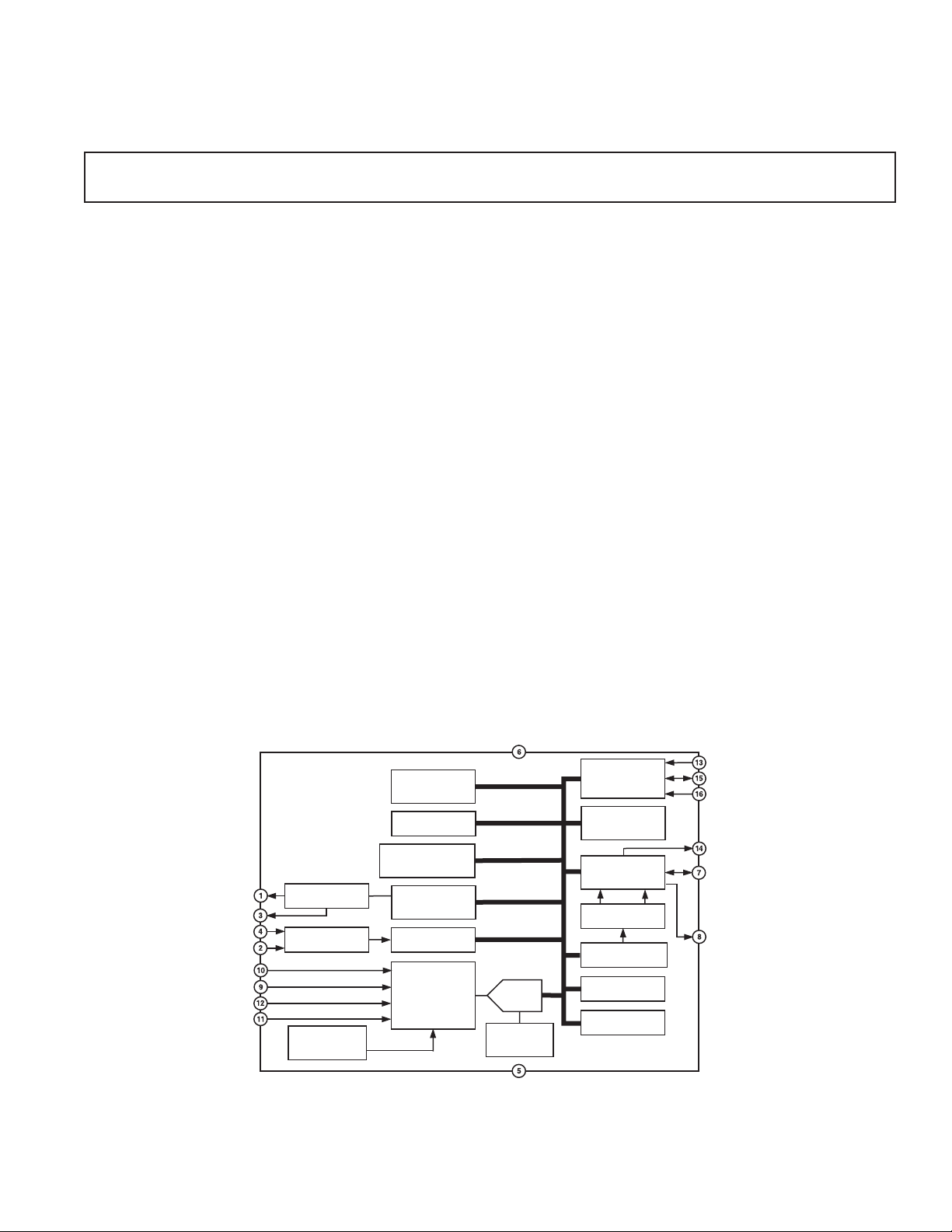
FUNCTIONAL BLOCK DIAGRAM
SLAVE
ADDRESS
REGISTER
FAN FILTER
REGISTER
FA N
CHARACTERISTICS
REGISTERS
FAN SPEED
CONFIG
REGISTER
FAN SPEED
COUNTER
ANALOG
MULTIPLEXER
*Patents pending.
PWM_OUT1
PWM_OUT2
TACH2 /AIN2
TACH1 /AIN1
D1+
D1–
D2+
D2–
ADM1031
PWM
CONTROLLERS
TACH SIGNAL
CONDITIONING
BANDGAP
TEMPERATURE
SENSOR
REV. A
Information furnished by Analog Devices is believed to be accurate and
reliable. However, no responsibility is assumed by Analog Devices for its
use, nor for any infringements of patents or other rights of third parties that
may result from its use. No license is granted by implication or otherwise
under any patent or patent rights of Analog Devices. Trademarks and
registered trademarks are the property of their respective companies.
V
CC
SERIAL BUS
INTERFACE
ADDRESS
POINTER
REGISTER
INTERRUPT
STATUS
REGISTERS
LIMIT
COMPARATOR
VA LUE AND LIMIT
REGISTERS
OFFSET
ADC
2.5V
BANDGAP
REFERENCE
GND
One Technology Way, P.O. Box 9106, Norwood, MA 02062-9106, U.S.A.
Tel: 781/329-4700 www.analog.com
Fax: 781/326-8703 © 2003 Analog Devices, Inc. All rights reserved.
REGISTERS
CONFIGURATION
REGISTERS
ADD
SDA
SCL
INT (SMBALERT)
THERM
FAN_FAULT
Page 2

ADM1031–SPECIFICATIONS
(TA = T
MIN
to T
, VCC = V
MAX
MIN
to V
, unless otherwise noted.)
MAX
1
Parameter Min Typ Max Unit Test Conditions/Comments
POWER SUPPLY
Supply Voltage, V
Supply Current, I
CC
CC
3.0 3.30 5.5 V
1.4 3 mA Interface Inactive, ADC Active
32 50 µA Standby Mode
TEMPERATURE-TO-DIGITAL CONVERTER
Local Sensor Accuracy ± 1 ± 3 °C
Resolution 0.25 °C
Remote Diode1 Sensor Accuracy ± 0.5 ± 1 °C60°C ≤ T
Remote Diode2 Sensor Accuracy ± 0.5 ± 1.75 °C60°C ≤ T
≤ 100°C
D
≤ 100°C
D
Resolution 0.125 °C
Remote Sensor Source Current 180 µA High Level
11 µA Low Level
OPEN-DRAIN DIGITAL OUTPUTS
(THERM, INT, FAN_FAULT, PWM_OUT)
Output Low Voltage, V
High-Level Output Leakage Current, I
OL
OH
0.4 V I
0.1 1 µAV
= –6.0 mA; V
OUT
= VCC; V
OUT
CC
= 3 V
CC
= 3 V
OPEN-DRAIN SERIAL DATA BUS OUTPUT (SDA)
Output Low Voltage, V
High-Level Output Leakage Current, I
OL
OH
0.4 V I
0.1 1 µAV
= –6.0 mA; V
OUT
= V
OUT
CC
CC
= 3 V
SERIAL BUS DIGITAL INPUTS (SCL, SDA)
Input High Voltage, V
Input Low Voltage, V
IL
IH
2.1 V
0.8 V
Hysteresis 500 mV
DIGITAL INPUT LOGIC LEVELS
2
(ADD, THERM, TACH1/2)
Input High Voltage, V
Input Low Voltage, V
IL
IH
2.1 V
0.8 V
DIGITAL INPUT LEAKAGE CURRENT
Input High Current, I
Input Low Current, I
Input Capacitance, C
IH
IL
IN
–1 µAV
1 µAV
5pF
IN
IN
= V
= 0
CC
FAN RPM-TO-DIGITAL CONVERTER
Accuracy ± 6% 60°C ≤ T
≤ 100°C
A
Full-Scale Count 255
TACH Nominal Input RPM 4400 RPM Divisor N = 1, Fan Count = 153
2200 RPM Divisor N = 2, Fan Count = 153
1100 RPM Divisor N = 4, Fan Count = 153
550 RPM Divisor N = 8, Fan Count = 153
Conversion Cycle Time 637 ms
SCLK
SW
BUF
SU;STA
HD;STA
LOW
HIGH
SU;DAT
HD;DAT
3
10 100 kHz See Figure 1
50 ns See Figure 1
4.7 µs See Figure 1
4.7 µs See Figure 1
4 µs See Figure 1
SU;STO
4 µs See Figure 1
1.3 µs See Figure 1
450µs See Figure 1
R
F
1000 ns See Figure 1
300 ns See Figure 1
250 ns See Figure 1
300 ns See Figure 1
= 0.8 V for a falling edge and V
IL
= 2.2 V for a rising edge.
IH
SERIAL BUS TIMING
Clock Frequency, f
Glitch Immunity, t
Bus Free Time, t
Start Setup Time, t
Start Hold Time, t
Stop Condition Setup Time t
SCL Low Time, t
SCL High Time, t
SCL, SDA Rise Time, t
SCL, SDA Fall Time, t
Data Setup Time, t
Data Hold Time, t
NOTES
1
Typicals are at TA = 25°C and represent most likely parametric norm. Shutdown current typ is measured with VCC = 3.3 V.
2
ADD is a three-state input that may be pulled high, low or left open-circuit.
3
Timing specifications are tested at logic levels of V
Specifications subject to change without notice.
–2–
REV. A
Page 3
ADM1031
ABSOLUTE MAXIMUM RATINGS*
Positive Supply Voltage (VCC) . . . . . . . . . . . . . . . . . . . . .6.5 V
Voltage on Any Input or Output Pin . . . . . . . . –0.3 V to +6.5 V
Input Current at Any Pin . . . . . . . . . . . . . . . . . . . . . . . ± 5 mA
Package Input Current . . . . . . . . . . . . . . . . . . . . . . . ± 20 mA
Maximum Junction Temperature (T
) . . . . . . . . . . 150°C
JMAX
Storage Temperature Range . . . . . . . . . . . . –65°C to +150°C
Lead Temperature, Soldering
Vapor Phase 60 sec . . . . . . . . . . . . . . . . . . . . . . . . . . 215°C
Infrared 15 sec . . . . . . . . . . . . . . . . . . . . . . . . . . . . . 200°C
ESD Rating All Pins . . . . . . . . . . . . . . . . . . . . . . . . . . 2000 V
*Stresses above those listed under Absolute Maximum Ratings may cause perma-
nent damage to the device. This is a stress rating only; functional operation of the
device at these or any other conditions above those indicated in the operational
section of this specification is not implied. Exposure to absolute maximum rating
conditions for extended periods may affect device reliability.
THERMAL CHARACTERISTICS
16-Lead QSOP Package
θ
= 105°C/W, θ
JA
SCL
= 39°C/W
JC
t
HD:STA
t
LOW
t
R
t
HD:DAT
t
HIGH
t
F
t
SU:DAT
ORDERING GUIDE
Temperature Package Package
Model Range Description Option
ADM1031ARQ 0°C to 100°C 16-Lead QSOP RQ-16
t
HD:STA
t
SU:STA
t
SU:STO
SDA
t
BUF
S
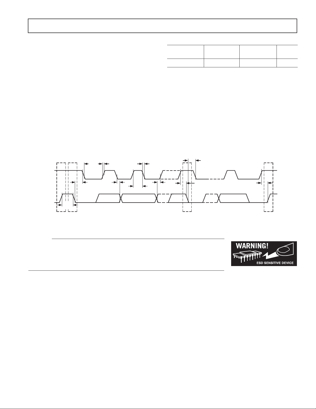
Figure 1. Diagram for Serial Bus Timing
CAUTION
ESD (electrostatic discharge) sensitive device. Electrostatic charges as high as 4000 V readily
accumulate on the human body and test equipment and can discharge without detection.
Although the ADM1031 features proprietary ESD protection circuitry, permanent damage may
occur on devices subjected to high energy electrostatic discharges. Therefore, proper ESD
precautions are recommended to avoid performance degradation or loss of functionality.
PSP
REV. A
–3–
Page 4

ADM1031
PIN FUNCTION DESCRIPTIONS
Pin No. Mnemonic Description
1 PWM_OUT1 Digital Output (Open-Drain). Pulsewidth modulated output to control fan speed. Requires pull-
up resistor (10 kΩ typical).
2 TACH1/AIN1 Digital/Analog Input. Fan tachometer input to measure FAN1 fan speed. May be reprogrammed as
an analog input to measure speed of a 2-wire fan via a sense resistor (2 Ω typical).
3 PWM_OUT2 Digital Output (Open-Drain). Pulsewidth Modulated output to control FAN2 fan speed.
Requires pull-up resistor (10 kΩ typical).
4 TACH2/AIN2 Digital/Analog Input. Fan tachometer input to measure FAN2 fan speed. May be repro-
grammed as an analog input to measure speed of a 2-wire fan via a sense resistor (2 Ω typical).
5GND System Ground.
6V
CC
7 THERM Digital I/O (Open-Drain). An active low thermal overload output that indicates a violation of a
8 FAN_FAULT Digital Output (Open-Drain). Can be used to signal a fan fault. Drives second fan to full speed
9 D1– Analog Input. Connected to cathode of first remote temperature-sensing diode. The temperature-
10 D1+ Analog Input. Connected to anode of first remote temperature-sensing diode.
11 D2– Analog Input. Connected to cathode of second remote temperature-sensing diode.
12 D2+ Analog Input. Connected to anode of second remote temperature-sensing diode.
13 ADD Three-State Logic Input. Sets two lower bits of device SMBus address.
14 INT (SMBALERT)Digital Output (Open-Drain). Can be programmed as an interrupt (SMBus ALERT) output for
15 SDA Digital I/O. Serial Bus Bidirectional Data. Open-drain output. Requires pull-up resistor
16 SCL Digital Input. Serial Bus Clock. Requires pull-up resistor (2.2 kΩ typical).
Power. Can be powered by 3.3 V Standby power if monitoring in low power states is required.
temperature set point (overtemperature). Also acts as an input to provide external fan control.
When this pin is pulled low by an external signal, a status bit is set, and the fan speed is set to
full-on. Requires pull-up resistor (10 kΩ).
if one fan fails. Requires pull-up resistor (typically 10 kΩ).
sensing element is either a Pentium III substrate transistor or a general-purpose 2N3904.
temperature/fan speed interrupts. Requires pull-up resistor (10 kΩ typical).
(2.2 kΩ typical).
PIN CONFIGURATION
GND
V
THERM
CC
1
2
3
ADM1031
4
TOP VIEW
5
(Not to Scale)
6
7
8
PWM_OUT1
TACH1/AIN1
PWM_OUT2
TACH2/AIN2
FAN_FAULT
SCL
16
SDA
15
INT(SMBALERT)
14
ADD
13
D2+
12
D2–
11
D1+
10
D1–
9
–4–
REV. A
Page 5
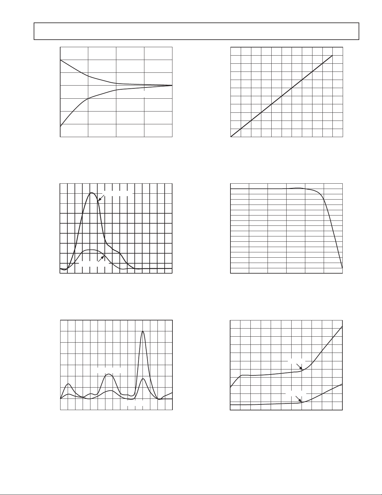
Typical Performance Characteristics–ADM1031
DXP – DXN CAPACITANCE – nF
–2
–10
1472.2
REMOTE TEMPERATURE ERROR – ⴗC
3.3
4.7
10 22
–3
–5
–7
–9
–6
1
–11
–12
–13
–14
–15
–16
0
–1
–4
–8
15
10
5
0
–5
–10
–15
REMOTE TEMPERATURE ERROR – ⴗC
–20
1
3.3
LEAKAGE RESISTANCE – M⍀
DXP TO GND
DXP TO VCC (3.3V)
10 30
100
TPC 1. Temperature Error vs. PCB Track Resistance
17
15
C
ⴗ
13
11
REMOTE TEMPERATURE ERROR –
–1
9
7
5
3
1
0
VIN = 200mV p-p
500k 2M
VIN = 100mV p-p
4M 6M 10M 100M 400M
FREQUENCY – Hz
110
100
90
80
70
60
50
READING – ⴗC
40
30
20
10
0
06010
20
40 50
30
PIII TEMPERATURE – ⴗC
70 80 90 100 110
TPC 4. Pentium III Temperature Measurement vs.
ADM1031 Reading
TPC 2. Temperature Error vs. Power Supply Noise
Frequency
7
6
C
ⴗ
5
4
3
2
1
REMOTE TEMPERATURE ERROR –
0
–1
0 400M100k 1M
VIN = 40mV p-p
200M 300M
100M
FREQUENCY – Hz
VIN = 20mV p-p
500M
TPC 3. Temperature Error vs. Common-Mode Noise
Frequency
REV. A
TPC 5. Temperature Error vs. Capacitance between
D+ and D–
110
100
90
80
A
70
60
50
40
SUPPLY CURRENT –
30
20
10
0
0751
25 50
10
5
SCLK FREQUENCY – kHz
VCC = 5V
VCC = 3.3V
100 250 500 750 1000
TPC 6. Standby Current vs. Clock Frequency
–5–
Page 6
ADM1031
7
6
5
4
3
2
1
REMOTE TEMPERATURE ERROR – ⴗC
0
–1
0 400M100k
VIN = 30mV p-p
VIN = 20mV p-p
1M
100M
FREQUENCY – Hz
200M 300M
500M
TPC 7. Temperature Error vs. Differential-Mode Noise
Frequency
200
180
160
140
120
100
80
60
SUPPLY CURRENT – A
40
20
0
–20
0 1.1 1.3 1.5 1.7 1.9 2.1
ADD = V
CC
SUPPLY VOLTAGE – V
ADD = GND
ADD = Hi-Z
2.9 4.5
2.5
0.08
0
–0.08
–0.16
–0.24
C
ⴗ
–0.32
–0.40
ERROR –
–0.48
–0.56
–0.64
–0.72
–0.80
20 40 60 80 85 100 105 120
0
TEMPERATURE – ⴗC
TPC 10. Remote Temperature Sensor Error
1.30
1.25
1.20
1.15
1.10
1.05
1.00
0.95
SUPPLY CURRENT – mA
0.90
0.85
0.80
2.0
2.8 3.2 3.6 4.0 4.4 4.82.2 2.6 3.0 3.4 3.8 4.2 4.6 5.0
2.4
SUPPLY VOLTAGE – V
TPC 8. Standby Supply Current vs. Supply Voltage
0.08
0
–0.08
–0.16
–0.24
C
ⴗ
–0.32
–0.40
ERROR –
–0.48
–0.56
–0.64
–0.72
–0.80
0
20 40 60 80 85 100 105 120
TEMPERATURE – ⴗC
TPC 9. Local Sensor Temperature Error
TPC 11. Supply Current vs. Supply Voltage
120
110
100
90
80
70
60
50
40
TEMPERATURE – ⴗC
30
20
10
0
0
2
4681013579
TIME – Sec
TPC 12. Response to Thermal Shock
–6–
REV. A
Page 7

ADM1031
GENERAL DESCRIPTION
The ADM1031 is a temperature monitor and dual PWM fan
controller for microprocessor-based systems. The device communicates with the system via a serial System Management Bus.
The serial bus controller has a hardwired address pin for device
selection (Pin 13), a serial data line for reading and writing
addresses and data (Pin 15), and an input line for the serial
clock (Pin 16). All control and programming functions of the
ADM1031 are performed over the serial bus. The device also
supports Alert Response Address (ARA).
INTERNAL REGISTERS OF THE ADM1031
A brief description of the ADM1031’s principal internal registers is given below. More detailed information on the function
of each register is given in Table XII to Table XXIX.
Configuration Register
Provides control and configuration of various functions on
the device.
Address Pointer Register
This register contains the address that selects one of the other
internal registers. When writing to the ADM1031, the first byte
of data is always a register address, which is written to the
Address Pointer Register.
Status Registers
These registers provide status of each limit comparison.
Value and Limit Registers
The results of temperature and fan speed measurements are
stored in these registers, along with their limit values.
Fan Speed Config Register
This register is used to program the PWM duty cycle for each fan.
Offset Registers
Allows the temperature channel readings to be offset by a 5-bit
two’s complement value written to these registers. These values
will automatically be added to the temperature values (or subtracted from if negative). This allows the systems designer to
optimize the system if required, by adding or subtracting up to
15°C from a temperature reading.
Fan Characteristics Registers
These registers are used to select the spin-up time, PWM frequency, and speed range for the fans used.
THERM Limit Registers
These registers contain the temperature values at which THERM
will be asserted.
T
MIN/TRANGE
Registers
These registers are read/write registers that hold the minimum
temperature value below which the fan will not run when the
device is in Automatic Fan Speed Control Mode. These registers
also hold the temperature range value that defines the range
over which auto fan control will be provided, and hence determines the temperature at which the fan will run at full speed.
SERIAL BUS INTERFACE
Control of the ADM1031 is carried out via the SMBus. The
ADM1031 is connected to this bus as a slave device, under the
control of a master device, e.g., the 810 chipset.
The ADM1031 has a 7-bit serial bus address. When the device
is powered up, it will do so with a default serial bus address.
The five MSBs of the address are set to 01011, the two LSBs
are determined by the logical state of Pin 13 (ADD). This is a
three-state input that can be grounded, connected to V
CC,
or left
open-circuit to give three different addresses. The state of the
ADD pin is only sampled at power-up, so changing ADD with
power on will have no effect until the device is powered off, then
on again.
Table I. ADD Pin Truth Table
ADD Pin A1 A0
GND 0 0
No Connect 1 0
V
CC
01
If ADD is left open-circuit, the default address will be 0101110.
The facility to make hardwired changes at the ADD pin allows
the user to avoid conflicts with other devices sharing the same
serial bus; for example, if more than one ADM1031 is used in
a system.
The serial bus protocol operates as follows:
1. The master initiates data transfer by establishing a START
condition, defined as a high-to-low transition on the serial
data line SDA while the serial clock line SCL remains high.
This indicates that an address/data stream will follow. All
slave peripherals connected to the serial bus respond to the
START condition, and shift in the next 8 bits, consisting
of a 7-bit address (MSB first) plus an R/W bit that determines the direction of the data transfer, i.e., whether data
will be written to or read from the slave device.
The peripheral whose address corresponds to the transmitted
address responds by pulling the data line low during the low
period before the ninth clock pulse, known as the Acknowledge Bit. All other devices on the bus now remain idle while
the selected device waits for data to be read from or written
to it. If the R/W bit is a 0, the master will write to the slave
device. If the R/W bit is a 1, the master will read from the
slave device.
2. Data is sent over the serial bus in sequences of nine clock
pulses, eight bits of data followed by an Acknowledge Bit
from the slave device. Transitions on the data line must
occur during the low period of the clock signal and remain
stable during the high period, as a low-to-high transition
when the clock is high may be interpreted as a STOP signal.
The number of data bytes that can be transmitted over the
serial bus in a single READ or WRITE operation is limited
only by what the master and slave devices can handle.
3. When all data bytes have been read or written, stop condi-
tions are established. In WRITE mode, the master will pull
the data line high during the tenth clock pulse to assert a
STOP condition. In READ mode, the master device will
override the acknowledge bit by pulling the data line high
during the low period before the ninth clock pulse. This is
known as No Acknowledge. The master will then take the
data line low during the low period before the tenth clock
pulse, then high during the tenth clock pulse to assert a
STOP condition.
Any number of bytes of data may be transferred over the serial
bus in one operation, but it is not possible to mix read and write
in one operation, because the type of operation is determined at
the beginning and cannot subsequently be changed without
starting a new operation.
REV. A
–7–
Page 8
ADM1031
In the case of the ADM1031, write operations contain either
one or two bytes, and read operations contain one byte, and
perform the following functions.
To write data to one of the device data registers or read data
from it, the Address Pointer Register must be set so that the
correct data register is addressed; data can then be written into
that register or read from it. The first byte of a write operation
always contains an address that is stored in the Address Pointer
Register. If data is to be written to the device, the write operation contains a second data byte that is written to the register
selected by the address pointer register.
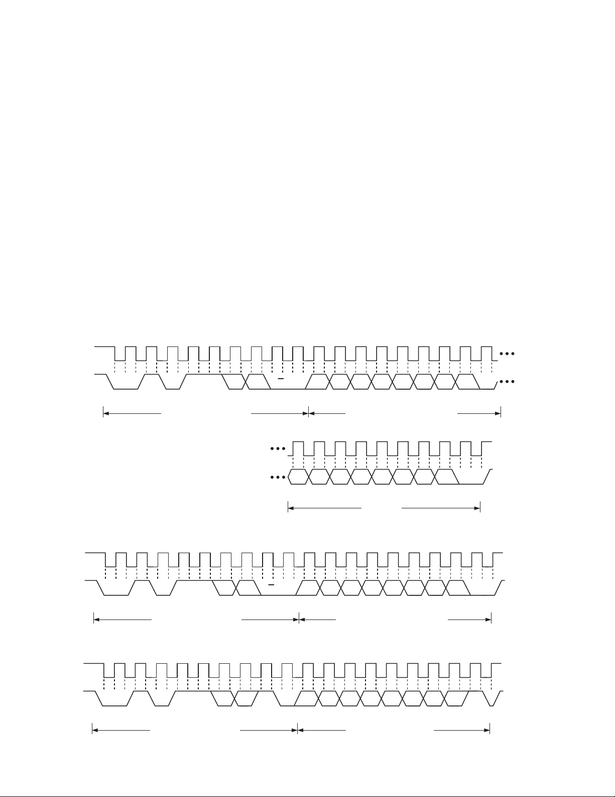
This is illustrated in Figure 2a. The device address is sent over
the bus followed by R/W set to 0. This is followed by two data
bytes. The first data byte is the address of the internal data
register to be written to, which is stored in the Address Pointer
Register. The second data byte is the data to be written to the
internal data register.
When reading data from a register there are two possibilities:
1. If the ADM1031’s Address Pointer Register value is unknown
or not the desired value, it is first necessary to set it to the
correct value before data can be read from the desired data
register. This is done by performing a write to the ADM1031
19
SCL
as before, but only the data byte containing the register address
is sent, as data is not to be written to the register. This is
shown in Figure 2b.
A read operation is then performed consisting of the serial bus
address, R/W bit set to 1, followed by the data byte read from
the data register. This is shown in Figure 2c.
2. If the Address Pointer Register is known to be already at the
desired address, data can be read from the corresponding
data register without first writing to the Address Pointer
Register, so Figure 2b can be omitted.
NOTES
1. Although it is possible to read a data byte from a data register
without first writing to the Address Pointer Register, if the
Address Pointer Register is already at the correct value, it is
not possible to write data to a register without writing to the
Address Pointer Register, because the first data byte of a
write is always written to the Address Pointer Register.
2. In Figures 2a to 2c, the serial bus address is shown as the
default value 01011(A1)(A0), where A1 and A0 are set by
the three-state ADD pin.
3. The ADM1031 also supports the Read Byte protocol, as
described in the System Management Bus specification.
1
9
SDA
START BY
MASTER
0
1011
SERIAL BUS ADDRESS BYTE
FRAME 1
SCL (CONTINUED)
SDA (CONTINUED)
A0
A1
R/W
ACK. BY
ADM1031
1
D7
D7
D6
D6
D5
D4
D5
ADDRESS POINTER REGISTER BYTE
D4
FRAME 2
D3
FRAME 3
DATA BYTE
D3
D2
D2
D1
D1
D0
D0
9
ACK. BY
ADM1031
ACK. BY
ADM1031
STOP BY
MASTER
Figure 2a. Writing a Register Address to the Address Pointer Register, then Writing Data to the Selected Register
D0
9
ACK. BY
ADM1031
STOP BY
MASTER
SCL
SDA
START BY
MASTER
19
0
1011
FRAME 1
SERIAL BUS ADDRESS BYTE
A0
A1
R/W
ACK. BY
ADM1031
1
D6
D7
ADDRESS POINTER REGISTER BYTE
D5
D4
FRAME 2
D3
D2
D1
Figure 2b. Writing to the Address Pointer Register Only
9
SCL
19
1
SDA
START BY
MASTER
0
1011
SERIAL BUS ADDRESS BYTE
FRAME 1
A0
A1
R/W
ACK. BY
ADM1031
D6
D7
D4
D5
FRAME 2
DATA BYTE FROM ADM1031
D3
D2
Figure 2c. Reading Data from a Previously Selected Register
–8–
D1
D0
NO ACK.
BY MASTER
STOP BY
MASTER
REV. A
Page 9
ADM1031
ALERT RESPONSE ADDRESS
Alert Response Address (ARA) is a feature of SMBus devices
that allows an interrupting device to identify itself to the host
when multiple devices exist on the same bus.
The INT output can be used as an interrupt output or can be used
as an SMBALERT. One or more INT outputs can be connected
to a common SMBALERT line connected to the master. If a
device’s INT line goes low, the following procedure occurs:
1. SMBALERT pulled low.
2. Master initiates a read operation and sends the Alert
Response Address (ARA = 0001 100). This is a general call
address that must not be used as a specific device address.
3. The device whose INT output is low responds to the Alert
Response Address, and the master reads its device address.
The address of the device is now known and can be interrogated in the usual way.
4. If more than one device’s INT output is low, the one with
the lowest device address will have priority, in accordance
with normal SMBus arbitration.
5. Once the ADM1031 has responded to the Alert Response
Address, it will reset its INT output; however, if the error
condition that caused the interrupt persists, INT will be
reasserted on the next monitoring cycle.
TEMPERATURE MEASUREMENT SYSTEM
Internal Temperature Measurement
The ADM1031 contains an on-chip bandgap temperature sensor. The on-chip ADC performs conversions on the output of
this sensor and outputs the temperature data in 10-bit two’s
complement format. The resolution of the local temperature
sensor is 0.25°C. The format of the temperature data is shown
in Table II.
External Temperature Measurement
The ADM1031 can measure the temperatures of two external
diode sensors or diode-connected transistors, connected to Pins
9 and 10 and Pins 11 and 12.
These pins are dedicated temperature input channels. The
function of Pin 7 is as a THERM input/output and is used to
flag overtemperature conditions.
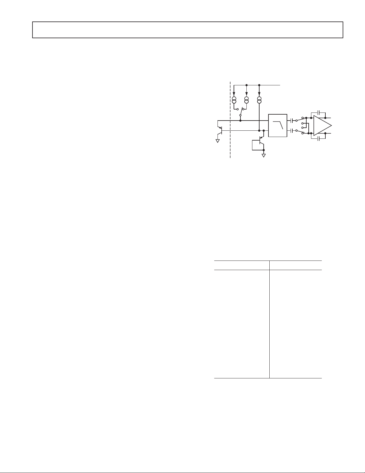
The forward voltage of a diode or diode-connected transistor,
operated at a constant current, exhibits a negative temperature
coefficient of about –2 mV/°C. Unfortunately, the absolute
value of V
, varies from device to device, and individual
BE
calibration is required to null this out, so the technique is
unsuitable for mass production.
The technique used in the ADM1031 is to measure the change
in V
when the device is operated at two different currents.
BE
This is given by:
∆V
= KT/q × ln (N)
BE
where:
K is Boltzmann’s constant.
q is charge on the carrier.
T is absolute temperature in Kelvins.
N is ratio of the two currents.
Figure 3 shows the input signal conditioning used to measure
the output of an external temperature sensor. This figure shows
the external sensor as a substrate transistor, provided for temperature monitoring on some microprocessors, but it could equally
well be a discrete transistor.
V
DD
REMOTE
SENSING
TRANSISTOR
IN ⴛ II
D+
D–
BIAS
DIODE
BIAS
LOW-PASS
f
FILTER
= 65kHz
C
V
V
OUT+
OUT–
TO
ADC
Figure 3. Signal Conditioning
If a discrete transistor is used, the collector will not be grounded,
and should be linked to the base. If a PNP transistor is used, the
base is connected to the D– input and the emitter to the D+
input. If an NPN transistor is used, the emitter is connected to
the D– input and the base to the D+ input.
One LSB of the ADC corresponds to 0.125°C, so the ADM1031
can theoretically measure temperatures from –127°C to +127.75°C,
although –127°C is outside the operating range for the device.
The extended temperature resolution data format is shown in
Tables III and IV.
Table II. Temperature Data Format (Local Temperature
and Remote Temperature High Bytes)
Temperature (ⴗC) Digital Output
–128°C 1000 0000
–125°C 1000 0011
–100°C 1001 1100
–75°C 1011 0101
–50°C 1100 1110
–25°C 1110 0111
–1°C 1111 1111
0°C 0000 0000
+1°C 0000 0001
+10°C 0000 1010
+25°C 0001 1001
+50°C 0011 0010
+75°C 0100 1011
+100°C 0110 0100
+125°C 0111 1101
+127°C 0111 1111
REV. A
–9–
Page 10

ADM1031
Table III. Remote Sensor Extended Temperature Resolution
Extended Remote Temperature
Resolution (ⴗC) Low Bits
0.000 000
0.125 001
0.250 010
0.375 011
0.500 100
0.625 101
0.750 110
0.875 111
The extended temperature resolution for the local and remote
channels is stored in the Extended Temperature Resolution
Register (Register 0x06), and is outlined in Table XVIII.
Table IV. Local Sensor Extended Temperature Resolution
Extended Local Temperature
Resolution (ⴗC) Low Bits
0.00 00
0.25 01
0.50 10
0.75 11
To prevent ground noise interfering with the measurement, the
more negative terminal of the sensor is not referenced to ground,
but biased above ground by an internal diode at the D– input. If
the sensor is used in a very noisy environment, a capacitor of
value up to 1000 pF may be placed between the D+ and D–
inputs to filter the noise.
To measure ∆V
, the sensor is switched between operating
ΒΕ
currents of I and N × I. The resulting waveform is passed through
a 65 kHz low-pass filter to remove noise, then to a chopperstabilized amplifier that performs the functions of amplification
and rectification of the waveform to produce a dc voltage proportional to ∆V
. This voltage is measured by the ADC to give
BE
a temperature output in 11-bit two’s complement format. To
further reduce the effects of noise, digital filtering is performed
by averaging the results of 16 measurement cycles. An external
temperature measurement nominally takes 9.6 ms.
LAYOUT CONSIDERATIONS
Digital boards can be electrically noisy environments and care
must be taken to protect the analog inputs from noise, particularly when measuring the very small voltages from a remote
diode sensor. The following precautions should be taken:
1. Place the ADM1031 as close as possible to the remote sensing diode. Provided that the worst noise sources such as clock
generators, data/address buses, and CRTs are avoided, this
distance can be 4 to 8 inches.
2. Route the D+ and D– tracks close together, in parallel, with
grounded guard tracks on each side. Provide a ground plane
under the tracks if possible.
3. Use wide tracks to minimize inductance and reduce noise pickup. 10 mil track minimum width and spacing is recommended.
GND
D+
D–
GND
10MIL
10MIL
10MIL
10MIL
10MIL
10MIL
10MIL
Figure 4. Arrangement of Signal Tracks
4. Try to minimize the number of copper/solder joints, which
can cause thermocouple effects. Where copper/solder joints
are used, make sure that they are in both the D+ and D–
path and at the same temperature.
Thermocouple effects should not be a major problem as 1°C
corresponds to about 200 µV, and thermocouple voltages are
about 3 µV/°C of temperature difference. Unless there are two
thermocouples with a big temperature differential between
them, thermocouple voltages should be much less than 200 µV.
5. Place a 0.1 µF bypass capacitor close to the ADM1031.
6. If the distance to the remote sensor is more than 8 inches, the
use of twisted pair cable is recommended. This will work up
to about 6 to 12 feet.
7. For really long distances (up to 100 feet) use shielded twisted
pair such as Belden #8451 microphone cable. Connect the
twisted pair to D+ and D– and the shield to GND close to
the ADM1031. Leave the remote end of the shield unconnected to avoid ground loops.
Because the measurement technique uses switched current
sources, excessive cable and/or filter capacitance can affect the
measurement. When using long cables, the filter capacitor C1
may be reduced or removed. In any case the total shunt capacitance should not exceed 1000 pF.
Cable resistance can also introduce errors. 1 Ω series resistance
introduces about 0.5°C error.
ADDRESSING THE DEVICE
ADD (Pin 13) is a three-state input. It is sampled, on power-up
to set the lowest two bits of the serial bus address. Up to three
addresses are available to the systems designer via this address
pin. This reduces the likelihood of conflicts with other devices
attached to the System Management Bus.
THE ADM1031 INTERRUPT SYSTEM
The ADM1031 has two interrupt outputs, INT and THERM.
These have different functions. INT responds to violations of
software programmed temperature limits and is maskable
(described in more detail later).
THERM is intended as a “fail-safe” interrupt output that cannot be masked. If the temperature is below the low temperature
limit, the INT pin will be asserted low to indicate an out-of-limit
condition. If the temperature exceeds the high temperature limit,
the INT pin will also be asserted low. A third limit; THERM
limit, may be programmed into the device to set the temperature
limit above which the overtemperature THERM pin will be
–10–
REV. A
Page 11

ADM1031
asserted low. The behavior of the high limit and THERM limit
is as follows:
1. Whenever the temperature measured exceeds the high tem-
perature limit, the INT pin is asserted low.
2. If the temperature exceeds the THERM limit, the THERM
output asserts low. This can be used to throttle the CPU
clock. If the THERM-to-Fan Enable bit (Bit 7 of THERM
behavior/revision register) is cleared to 0, the fans will not
run full-speed. The THERM limit may be programmed at
a lower temperature than the high temperature limit. This
allows the system to run in silent mode, where the CPU can
be throttled while the cooling fan is off. If the temperature
continues to increase, and exceeds the high temperature limit,
an INT is generated. Software may then decide whether the
fan should run to cool the CPU. This allows the system to
run in SILENT MODE.
3. If the THERM-to-Fan Enable bit is set to 1, the fan will run
full-speed whenever THERM is asserted low. In this case,
both throttling and active cooling take place. If the high
temperature limit is programmed to a lower value than the
THERM limit, exceeding the high temperature limit will
assert INT low. Software could change the speed of the fan
depending on temperature readings. If the temperature continues to increase and exceeds the THERM limit, THERM
asserts low to throttle the CPU and the fan runs full-speed.
This allows the system to run in PERFORMANCE MODE,
where active cooling takes place and the CPU is only throttled
at high temperature.
Using the high temperature limit and the THERM limit in this
way allows the user to gain maximum performance from the system
by only slowing it down, should it be at a critical temperature.
Although the ADM1031 does not have a dedicated Interrupt
Mask Register, clearing the appropriate enable bits in Configuration Register 2 will clear the appropriate interrupts and mask
out future interrupts on that channel. Disabling interrupt bits
will prevent out-of-limit conditions from generating an interrupt
or setting a bit in the Status Registers.
USING THERM AS AN INPUT
The THERM pin is an open-drain input/output pin. When
used as an output, it signals overtemperature conditions. When
asserted low as an output, the fan will be driven full-speed if the
THERM-to-Fan Enable bit is set to 1 (Bit 7 of Register 0x3F).
When THERM is pulled low as an input, the THERM bit (Bit 7)
of Status Register 2 is set to 1, and the fans are driven full-speed.
Note that the THERM-to-Fan Enable bit has no effect whenever THERM is used as an input. If THERM is pulled low as
an input, and the THERM-to-Fan Enable bit = 0, the fans will
still be driven full-speed. The THERM-to-Fan Enable bit only
affects the behavior of THERM when used as an output.
STATUS REGISTERS
All out-of-limit conditions are flagged by status bits in Status
Registers 1 and 2 (0x02, 0x03). Bits 0 and 1 (Alarm Speed, Fan
Fault) of Status Register 1, once set, may be cleared by reading
Status Register 1. Once the Alarm Speed bit is cleared, this bit
will not be reasserted on the next monitoring cycle even if the
condition still persists. This bit may be reasserted only if the
fan is no longer at Alarm Speed. Bit 1 (Fan Fault) is set whenever a fan tach failure is detected.
Once cleared, it will reassert on subsequent fan tach failures.
Bits 2 and 3 of Status Registers 1, 2 are the Remote 1, 2 Temperature High and Low status bits. Exceeding the high or low
temperature limits for the external channel sets these status bits.
Reading the status register clears these bits. However, these bits
will be reasserted if the out-of limit condition still exists on the next
monitoring cycle. Bits 6 and 7 are the Local Temperature High
and Low status bits. These behave exactly the same as the Remote
Temperature High and Low status bits. Bit 4 of Status Register 1 indicates that the Remote Temperature THERM limit
has been exceeded. This bit gets cleared on a read of Status
Register 1 (see Figure 5). Bit 5 indicates a Remote Diode Error.
This bit will be a 1 if a short or open is detected on the Remote
Temperature channel on power-up. If this bit is set to 1 on
power-up, it cannot be cleared. Bit 6 of Status Register 2 (0x03)
indicates that the Local THERM limit has been exceeded. This bit
is cleared on a read of Status Register 2. Bit 7 indicates that
THERM has been pulled low as an input. This bit can also
be cleared on a read of Status Register 2.
THERM LIMIT
5ⴗ
TEMP
THERM
INT REARMED
INT
STATUS REG. READ
Figure 5. Operation of
THERM
and
INT
Signals
Figure 5 shows the interaction between INT and THERM.
Once a critical temperature THERM limit is exceeded, both
INT and THERM assert low. Reading the Status Registers
clears the interrupt and the INT pin goes high. However, the
THERM pin remains asserted until the measured temperature
falls 5
°
C below the exceeded THERM limit. This feature can be
used to CPU throttle or drive a fan full speed for maximum
cooling. Note, that the INT pin for that interrupt source is not
rearmed until the temperature has fallen below the THERM
limit –5
°
C. This prevents unnecessary interrupts from tying up
valuable CPU resources.
MODES OF OPERATION
The ADM1031 has four different modes of operation. These
modes determine the behavior of the system.
1. Automatic Fan Speed Control Mode.
2. Filtered Automatic Fan Speed Control Mode.
3. PWM Duty Cycle Select Mode (directly sets fan speed under
software control).
4. RPM Feedback Mode.
REV. A
–11–
Page 12

ADM1031
AUTOMATIC FAN SPEED CONTROL
The ADM1031 has a local temperature channel and two remote
temperature channels, which may be connected to an on-chip
diode-connected transistor on a CPU. These three temperature
channels may be used as the basis for an automatic fan speed
control loop to drive fans using Pulsewidth Modulation (PWM).
HOW DOES THE CONTROL LOOP WORK?
The Automatic Fan Speed Control Loop is shown in Figure 6.
MAX
FA N
SPEED
SPIN-UP FOR TWO SECONDS
100
C
ⴗ
93
= 5
C
87
80
73
66
60
PWM DUTY CYCLE – %
53
47
40
33
0
T
MIN
ⴗ
RANGE
= 10
RANGE
T
RANGE
T
C
ⴗ
= 20
T
510 20 40 60 80
C
ⴗ
= 40
RANGE
T
C
ⴗ
= 80
RANGE
T
TEMPERATURE – ⴗC
T
MAX
= T
MIN
+ T
RANGE
MIN
T
= T
T
MIN
TEMPERATURE
MAX
MIN
+ T
RANGE
Figure 6. Automatic Fan Speed Control
In order for the fan speed control loop to work, certain loop
parameters need to be programmed into the device.
1. T
. The temperature at which the fan should switch on
MIN
and run at minimum speed. The fan will only turn on once
the temperature being measured rises above the T
MIN
value
programmed. The fan will spin up for a predetermined time
(default = 2 secs). See Fan Spin-Up section for more details.
2. T
. The temperature range over which the ADM1031
RANGE
will automatically adjust the fan speed. As the temperature
increases beyond T
increased accordingly. The T
, the PWM_OUT duty cycle will be
MIN
parameter actually defines
RANGE
the fan speed versus temperature slope of the control loop.
3. T
The temperature at which the fan will be at its maxi-
MAX.
mum speed. At this temperature, the PWM duty cycle driving
the fan will be 100%. T
is given by T
MAX
Since this parameter is the sum of the T
MIN
MIN
+ T
and T
RANGE
RANGE
.
parameters, it does not need to be programmed into a
register on-chip.
4. A hysteresis value of 5
°
C is included in the control loop to
prevent the fan continuously switching on and off if the temperature is close to T
such time as the temperature drops 5
. The fan will continue to run until
MIN
°
C below T
MIN
.
Figure 7 shows the different control slopes determined by the
T
value chosen, and programmed into the ADM1031.
RANGE
T
was set to 0°C to start all slopes from the same point. It
MIN
can be seen how changing the T
value affects the PWM
RANGE
duty cycle versus temperature slope.
Figure 7. PWM Duty Cycle vs. Temperature Slopes (T
Figure 8 shows how, for a given T
value affects the loop. Increasing the T
the T
since T
(temperature at which the fan runs full speed) value,
MAX
MAX
= T
MIN
+ T
. Note, however, that the PWM
RANGE
, changing the T
RANGE
value will increase
MIN
RANGE
MIN
)
Duty Cycle vs Temperature slope remains exactly the same.
Changing the T
may be changed in increments of 4°C.
T
MIN
100
93
87
80
73
66
60
PWM DUTY CYCLE – %
53
47
40
33
0
T
MIN
Figure 8. Effect of Increasing T
value merely shifts the control slope. The
MIN
C
ⴗ
= 40
RANGE
T
20 40 60 80
TEMPERATURE – ⴗC
C
ⴗ
= 40
RANGE
T
Value on Control Loop
MIN
T
T
MAX
= 40
RANGE
= T
MIN
C
ⴗ
+ T
RANGE
FAN SPIN-UP
As was previously mentioned, once the temperature being measured exceeds the T
value programmed, the fan will turn on
MIN
at minimum speed (default = 33% duty cycle). However, the
problem with fans being driven by PWM is that 33% duty cycle
is not enough to reliably start the fan spinning. The solution is
to spin the fan up for a predetermined time, and once the fan
has spun up, its running speed may be reduced in line with the
temperature being measured.
The ADM1031 allows fan spin-up times between 200 ms and
8 seconds. Bits <2:0> of Fan Characteristics Registers 1 and
2 (Register 0x20, 0x21) program the fan spin-up times.
–12–
REV. A
Page 13

Once the Automatic Fan Speed Control Loop parameters have been
LOCAL TEMPERATURE – ⴗC
PWM DUTY CYCLE – %
0
100
93
87
80
73
66
60
53
47
40
33
T
MIN
20 40 60
T
RANGE
= 40
ⴗ
C
T
MAX
= T
MIN
+ T
RANGE
chosen, the ADM1031 device may be programmed. The ADM1031
is placed into Automatic Fan Speed Control Mode by setting Bit 7
of Configuration Register 1 (Register 0x00). The device powers up
in Automatic Fan Speed Control Mode by default. The control
mode offers further flexibility in that the user can decide which
temperature channel/channels control each fan.
Bits 6, 5 Control Operation (Config Register 1)
00 Remote Temp 1 Controls Fan 1. Remote Temp 2
01 Remote Temp 1 Controls Fans 1 and 2.
10 Remote Temp 2 Controls Fans 1 and 2.
11 Maximum Speed Calculated by Local and Remote
When Bits 5 and 6 of Config Register 1 are both set to 1, it offers
increased flexibility. The local and remote temperature channels
can have independently programmed control loops with different
control parameters. Whichever control loop calculates the fastest fan
speed based on the temperature being measured, drives the fans.
Figure 9 shows how the fan’s PWM duty cycle is determined by
two independent control loops. This is the type of Auto Mode Fan
Behavior seen when Bits 5 and 6 of Config Register 1 are set to 11.
Figure 9a shows the control loop for the Local Temperature channel. Its T
value is 40°C. The local temperature’s T
Figure 9b shows the control loop for the Remote Temperature channel. Its T
Therefore, the Remote Temperature’s T
Consider if both temperature channels measure 40°C. Both control
loops will calculate a PWM duty cycle of 66%. Therefore, the fan
will be driven at 66% duty cycle.
If both temperature channels measure 20°C, the local channel will
calculate 33% PWM duty cycle, while the Remote 1 channel will
calculate 50% PWM duty cycle. Thus, the fans will be driven at
50% PWM duty cycle. Consider the local temperature measuring
60°C while the Remote 1 temperature is measuring 70°C. The
PWM duty cycle calculated by the local temperature control loop
will be 100% (since the temperature = T
calculated by the Remote 1 temperature control loop at 70°C will
be approximately 90%. So the fan will run full-speed (100% duty
cycle). Remember, that the fan speed will be based on the fastest
speed calculated, and is not necessarily based on the highest
temperature measured. Depending on the control loop parameters programmed, a lower temperature on one channel, may
actually calculate a faster speed, than a higher temperature on
the other channel.
REV. A
Table V. Fan Spin-Up Times
Spin-Up Time
Bits 2:0 (Fan Characteristics Registers 1, 2)
000 200 ms
001 400 ms
010 600 ms
011 800 ms
100 1 sec
101 2 secs (Default)
110 4 secs
111 8 secs
Table VI. Auto Mode Fan Behavior
Controls Fan 2.
Temperature Channels Controls Fans 1 and 2.
value has been programmed to 20°C, and its T
MIN
value has been set to 0°C, while its T
MIN
will thus be 60°C.
MAX
RANGE
value will be 80°C.
MAX
). The PWM duty cycle
MAX
RANGE
= 80°C.
ADM1031
a.
100
93
87
80
73
66
60
PWM DUTY CYCLE – %
53
47
40
33
0
T
MIN
20 40 8070
REMOTE TEMPERATURE – ⴗC
T
b.
Figure 9. Max Speed Calculated by Local and Remote
Temperature Control Loops Drives Fan
PROGRAMMING THE AUTOMATIC FAN SPEED CONTROL LOOP
1. Program a value for T
2. Program a value for the slope T
3. T
MAX
= T
MIN
+ T
MIN
RANGE
.
RANGE
.
4. Program a value for Fan Spin-up Time.
5. Program the desired Automatic Fan Speed Control Mode
Behavior, i.e., which temperature channel controls the fan.
6. Select Automatic Fan Speed Control Mode by setting Bit 7
of Configuration Register 1.
OTHER CONTROL LOOP PARAMETERS
Having programmed all the above loop parameters, are there
any other parameters to worry about?
T
was defined as the temperature at which the fan switched
MIN
on and ran at minimum speed. This minimum speed is 33% duty
cycle by default. If the minimum PWM duty cycle is programmed
to 33%, the fan control loops will operate as previously described.
–13–
RANGE
= 80
.
C
ⴗ
T
= T
MAX
MIN
+ T
RANGE
Page 14

ADM1031
It should be noted however, that changing the minimum PWM
duty cycle affects the control loop behavior.
Slope 1 of Figure 10 shows T
set to 0°C and the T
MIN
RANGE
chosen
is 40°C. In this case, the fan’s PWM duty cycle will vary over the
range 33% to 100%. The fan will run full-speed at 40°C. If the
minimum PWM duty cycle at which the fan runs at T
is changed,
MIN
its effect can be seen on Slopes 2 and 3. Take Case 2, where
the minimum PWM duty cycle is reprogrammed from 33%
(default) to 53%.
100
93
87
80
73
66
60
PWM DUTY CYCLE – %
53
47
40
33
T
MIN
16 28 40 600
TEMPERATURE – ⴗC
RANGE
T
= 40
C
ⴗ
Figure 10. Effect of Changing Minimum Duty Cycle on
Control Loop with Fixed T
MIN
and T
RANGE
Values
The fan will actually reach full speed at a much lower temperature;
28°C. Case 3 shows that when the minimum PWM duty cycle was
increased to 73%, the temperature at which the fan ran full speed
was 16°C. So the effect of increasing the minimum PWM duty cycle,
with a fixed T
MIN
reach full speed (T
How can T
be calculated?
MAX
and fixed T
) at a lower temperature than T
MAX
, is that the fan will actually
RANGE
MIN
+ T
RANGE
.
In Automatic Fan Speed Control Mode, the register that holds the
minimum PWM duty cycle at T
, is the Fan Speed Config
MIN
Register (Register 0x22). Table VII shows the relationship between
the decimal values written to the Fan Speed Config Register and PWM
duty cycle obtained.
Table VII. Programming PWM Duty Cycle
Decimal Value PWM Duty Cycle
00 0%
01 7%
02 14%
03 20%
04 27%
05 33% (Default)
06 40%
07 47%
08 53%
09 60%
10 (0x0A) 67%
11 (0x0B) 73%
12 (0x0C) 80%
13 (0x0D) 87%
14 (0x0E) 93%
15 (0x0F) 100%
The temperature at which the fan will run full-speed (100%
duty cycle) is given by:
T
MAX
= T
+ ((Max DC – Min DC) × T
MIN
RANGE
/10)
where,
T
T
MAX
MIN
=Temperature at which fan runs full-speed.
=Temperature at which fan will turn on.
Max DC =Maximum Duty Cycle (100%) = 15 decimal.
Min DC =Duty Cycle at T
, programmed in to Fan Speed
MIN
Config Register (default = 33% = 5 decimal).
T
RANGE
=PWM Duty Cycle versus Temperature Slope.
Example 1
T
MIN
=0°C, T
RANGE
= 40°C
Min DC = 53% = 8 Decimal (Table VII)
Calculate T
T
MAX
T
MAX
T
MAX
T
MAX
.
MAX
=T
+ ((Max DC – Min DC) × T
MIN
RANGE
=0 + ((100% DC – 53% DC) × 40/10)
=0 + ((15 – 8) × 4) = 28
=28ⴗC (As seen on Slope 2 of Figure 10)
/10)
Example 2
T
MIN
=0°C, T
RANGE
= 40°C
Min DC = 73% = 11 Decimal (Table VII)
Calculate T
T
MAX
T
MAX
T
MAX
T
MAX
.
MAX
=T
+ ((Max DC – Min DC) × T
MIN
RANGE
=0 + ((100% DC – 73% DC) × 40/10)
=0 + ((15 – 11) × 4) = 16
=16ⴗC (As seen on Slope 3 of Figure 10)
/10)
Example 3
T
MIN
=0°C, T
RANGE
= 40°C
Min DC = 33% = 5 Decimal (Table VII)
Calculate T
T
MAX
T
MAX
T
MAX
T
MAX
.
MAX
=T
+ ((Max DC – Min DC) × T
MIN
RANGE
=0 + ((100% DC – 33% DC) × 40/10)
=0 + ((15 – 5) × 4) = 40
=40ⴗC (As seen on Slope 1 of Figure 10)
/10)
In this case, since the Minimum Duty Cycle is the default 33%,
the equation for T
T
T
T
T
MAX
MAX
MAX
MAX
=T
=T
=T
=T
reduces to:
MAX
+ ((Max DC – Min DC) × T
MIN
+ ((15 – 5) × T
MIN
+ (10 × T
MIN
+ T
MIN
RANGE
RANGE
RANGE
/10)
/10)
RANGE
/10)
–14–
REV. A
Page 15

ADM1031
RELEVANT REGISTERS FOR AUTOMATIC FAN SPEED
CONTROL MODE
Register 0x00 Configuration Register 1
<7> Logic 1 selects Automatic Fan Speed Control, Logic 0
selects software control (Default = 1).
<6:5> 00 = Remote Temp 1 controls Fan 1, Remote Temp 2
controls Fan 2.
01 = Remote Temp 1 controls Fans 1 and 2
10 = Remote Temp 2 controls Fans 1 and 2
11 = Fastest Calculated Speed controls Fans 1 and 2
Register 0x20, 0x21 Fan Characteristics Registers 1, 2
<2:0> Fan X Spin-Up Time
000 = 200 ms
001 = 400 ms
010 = 600 ms
011 = 800 ms
100 = 1 sec
101 = 2 secs (Default)
110 = 4 secs
111 = 8 secs
<5:3> PWM Frequency Driving the Fan
000 = 11.7 Hz
001 = 15.6 Hz
010 = 23.4 Hz
011 = 31.25 Hz (Default)
100 = 37.5 Hz
101 = 46.9 Hz
110 = 62.5 Hz
111 = 93.5 Hz
<7:6> Speed Range N; defines the lowest fan speed that can be
measured by the device.
00 = 1: Lowest Speed = 2647 RPM
01 = 2: Lowest Speed = 1324 RPM
10 = 4: Lowest Speed = 662 RPM
11 = 8: Lowest Speed = 331 RPM
Register 0x22 Fan Speed Configuration Register
<3:0> Min Speed: This nibble contains the speed at which the
fan will run when the temperature is at T
. The default is
MIN
0x05, meaning that the fan will run at 33% duty cycle
when the temperature is at T
MIN
.
<7:4> Min Speed: Determines the minimum PWM cycle for
Fan 2 in Automatic Fan Speed Control Mode.
Register 0x24 Local Temperature T
<7:3> Local Temperature T
MIN
MIN/TRANGE
. These bits set the temperature
at which the fan will turn on when under Auto Fan Speed
Control. T
can be programmed in 4°C increments.
MIN
00000 = 0°C
00001 = 4°C
00010 = 8°C
00011 = 12°C
|
|
01000 = 32°C (Default)
|
|
11110 = 120°C
11111 = 124°C
<2:0> Local Temperature T
. This nibble sets the tem-
RANGE
perature range over which Automatic Fan Speed Control
takes place.
000 = 5°C
001 = 10°C
010 = 20°C
011 = 40°C
100 = 80°C
Register 0x25, 0x26 Remote 1, 2 Temperature T
<7:3> Remote Temperature T
. Sets the temperature at
MIN
MIN/TRANGE
which the fan will switch on based on Remote X Temperature Readings.
00000 = 0°C
00001 = 4°C
00010 = 8°C
00011 = 12°C
|
|
01100 = 48°C
|
|
°
11110 = 120
11111 = 124
<2:0> Remote Temperature T
C
°
C
. This nibble sets the tem-
RANGE
perature range over which the fan will be controlled
based on Remote Temperature readings.
000 = 5°C
001 = 10°C
010 = 20°C
011 = 40°C
100 = 80°C
REV. A
–15–
Page 16

ADM1031
FILTERED CONTROL MODE
The Automatic Fan Speed Control Loop reacts instantaneously
to changes in temperature, i.e., the PWM duty cycle will respond
immediately to temperature change. In certain circumstances,
we may not want the PWM output to react instantaneously to
temperature changes. If significant variations in temperature
were found in a system, this would have the effect of changing
the fan speed, which could be obvious to someone in close proximity. One way to improve the system’s acoustics would be to
slow down the loop so that the fan ramps slowly to its newly
calculated fan speed. This also ensures that temperature transients
will effectively be ignored, and the fan’s operation will be smooth.
There are two means by which to apply filtering to the Automatic Fan Speed Control Loop. The first method is to ramp the
fan speed at a predetermined rate, to its newly calculated value
instead of jumping directly to the new fan speed. The second
approach involves changing the on-chip ADC sample rate, to
change the number of temperature readings taken per second.
The filtered mode on the ADM1031 is invoked by setting Bit 0
of the Fan Filter Register (Register 0x23) for Fan 1 and Bit 1
for Fan 2. Once the Fan Filter Register has been written to, and
all other control loop parameters (T
been programmed, the device may be placed into Automatic
Fan Speed Control Mode by setting Bit 7 of Configuration
Register 1 (Register 0x00) to 1.
Effect of Ramp Rate on Filtered Mode
Bits <6:5> of the Fan Filter Register determine the ramp rate in
Filtered Mode. The PWM_OUT signal driving the fan will have
a period, T, given by the PWM_OUT drive frequency, f, since
T = 1/f. For a given PWM period, T, the PWM period is subdivided in to 240 equal time slots. One time slot corresponds to
the smallest possible increment in PWM duty cycle. A PWM
signal of 33% duty cycle will thus be high for 1/3 × 240 time
slots and low for 2/3 × 240 time slots. Therefore, 33% PWM
duty cycle corresponds to a signal which is high for 80 time slots
and low for 160 time slots.
MIN
, T
RANGE
, etc.) have
READ
TEMPERATURE
CALCULATE
NEW PWM
DUTY CYCLE
DECREMENT
YES
NO
PREVIOUS
PWM VALUE
BY RAMP
RATE
IS NEW
PWM VALUE >
PREVIOUS
VALUE?
INCREMENT
PREVIOUS PWM
VALUE BY RAMP
RATE
Figure 12. Filtered Mode Algorithm
The Filtered Mode algorithm calculates a new PWM duty cycle
based on the temperature measured. If the new PWM duty cycle
value is greater than the previous PWM value, the previous
PWM duty cycle value is incremented by either 1, 2, 4, or 8
time slots (depending on the setting of bits <6:5> of the Fan
Filter Register). If the new PWM duty cycle value is less than
the previous PWM value, the previous PWM duty cycle is decremented by 1, 2, 4, or 8 time slots. Each time the PWM
duty cycle is incremented or decremented, it is stored as the
previous PWM duty cycle for the next comparison.
So what does an increase of 1, 2, 4, or 8 time slots actually mean
in terms of PWM duty cycle?
A Ramp Rate of 1 corresponds to one time slot, which is 1/240
of the PWM period. In Filtered Auto Fan Speed Control Mode,
incrementing or decrementing by 1 changes the PWM output
duty cycle by 0.416%.
PWM_OUT
33% DUTY
CYCLE
80 TIME
SLOTS
160 TIME
PWM OUTPUT
(ONE PERIOD) =
240 TIME SLOTS
SLOTS
Figure 11. 33% PWM Duty Cycle Represented in Time
Slots
The ramp rates in Filtered Mode are selectable between 1, 2,
4, and 8. The ramp rates are actually discrete time slots. For
example, if the ramp rate = 8, then eight time slots will be added to
the PWM_OUT high duty cycle each time the PWM_OUT duty
cycle needs to be increased. Figure 12 shows how the Filtered
Mode algorithm operates.
–16–
Table VIII. Effect of Ramp Rates on PWM_OUT
Ramp Rate PWM Duty Cycle Change
1 0.416%
2 0.833%
4 1.66%
8 3.33%
So programming a ramp rate of 1, 2, 4, or 8 simply increases
or decreases the PWM duty cycle by the amounts shown in
Table VIII, depending on whether the temperature is increasing or decreasing.
Figure 13 shows remote temperature plotted against PWM duty
cycle for Filtered Mode. The ADC sample rate is the highest
sample rate; 11.25 kHz. The ramp rate is set to 8 which would
correspond to the fastest ramp rate. With these settings it took
approximately 12 seconds to go from 0% duty cycle to 100%
duty cycle (full-speed). The T
value = 32°C and the T
MIN
RANGE
= 80°C. It can be seen that even though the temperature increased
very rapidly, the fan gradually ramps up to full speed.
REV. A
Page 17

ADM1031
ⴗ
TIME – s
0 112
120
80
40
60
20
0
140
80
60
40
20
0
110
120
100
PWM DUTY CYCLE – %
R
TEMP
– ⴗC
R
TEMP
PWM DUTY CYCLE
140
120
100
C
ⴗ
80
–
TEMP
60
R
40
20
0
012
R
Figure 13. Filtered Mode with Ramp Rate = 8
Figure 14 shows how changing the ramp rate from 8 to 4 affects
the control loop. The overall response of the fan is slower. Since
the ramp rate is reduced, it takes longer for the fan to achieve full
running speed. In this case, it took approximately 22 seconds for
the fan to reach full speed.
120
110
R
80
C
ⴗ
–
60
TEMP
R
40
20
0
022
TEMP
Figure 14. Filtered Mode with Ramp Rate = 4
Figure 15 shows the PWM output response for a ramp rate of
2. In this instance the fan took about 54 seconds to reach full
running speed.
140
120
100
C
80
–
TEMP
R
60
40
20
0
054
Figure 15. Filtered Mode with Ramp Rate = 2
REV. A
R
TEMP
TEMP
PWM DUTY CYCLE
TIME – s
PWM DUTY CYCLE
TIME – s
PWM DUTY CYCLE
TIME – s
120
100
80
60
40
PWM DUTY CYCLE – %
20
0
140
120
100
80
60
PWM DUTY CYCLE – %
40
20
0
120
100
80
60
40
PWM DUTY CYCLE – %
20
0
–17–
Finally, Figure 16 shows how the control loop reacts to temperature with the slowest ramp rate. The ramp rate is set to 1,
while all other control parameters remain the same. With the
slowest ramp rate selected it took 112 seconds for the fan to
reach full speed.
Figure 16. Filtered Mode with Ramp Rate = 1
As can be seen from Figures 13 through 16, the rate at which
the fan will react to temperature change is dependent on the
ramp rate selected in the Fan Filter Register. The higher the
ramp rate, the faster the fan will reach the newly calculated
fan speed.
Figure 17 shows the behavior of the PWM output as temperature varies. As the temperature is rising, the fan speed will ramp
up. Small drops in temperature will not affect the ramp-up
function since the newly calculated fan speed will still be higher
than the previous PWM value. The Filtered Mode allows the
PWM output to be made less sensitive to temperature variations. This will be dependent on the ramp rate selected and
the ADC sample rate programmed into the Fan Filter Register.
90 90
80 80
70 70
60 60
50 50
40 40
30 30
PWM DUTY CYCLE – %
20 20
10 10
00
PWM DUTY CYCLE
R
TEMP
TIME – s
C
ⴗ
–
TEMP
R
Figure 17. How Fan Reacts to Temperature Variation in
Filtered Mode
Page 18

ADM1031
Effect of ADC Sample Rate on Filtered Mode
The second means by which to change the Filtered Mode characteristics is to adjust the ADC sample rate. The faster the ADC
sample rate, the more temperature samples are obtained per second. One way to apply filtering to the control loop is to slow down
the ADC sampling rate. This means that the number of iterations
of the Filtered Mode algorithm per second is effectively reduced.
If the number of temperature measurements per second is
reduced, how often the PWM_OUT signal controlling the fan is
updated is also reduced.
Bits <4:2> of the Fan Filter Register (Reg 0x23) set the ADC
sample rate. The default ADC sample rate is 1.4 kHz. The ADC
sample rate is selectable from 87.5 Hz to 11.2 kHz. Table IX
shows how many temperature samples are obtained per second,
for each of the ADC sample rates.
Table IX. Temperature Updates per Second
ADC Sample Rate Temperature Updates/Sec
87.5 Hz 0.0625
175 Hz 0.125
350 Hz 0.25
700 Hz 0.5
1.4 kHz 1 (Default)
2.8 kHz 2
5.6 kHz 4
11.2 kHz 8
RELEVANT REGISTERS FOR FILTERED AUTOMATIC FAN SPEED CONTROL MODE
In addition to the registers used to program the normal Automatic Fan Speed Control Mode, the following register needs to
be programmed.
Register 0x23 Fan Filter Register
<7> Spin-up Disable :- when this bit is set to 1, fan spin-up
is disabled. (Default = 0)
<6:5> Ramp Rate: these bits set the ramp rate for filtered mode.
00 = 1 (0.416% Duty Cycle Change)
01 = 2 (0.833% Duty Cycle Change)
10 = 4 (1.66% Duty Cycle Change)
11 = 8 (3.33% Duty Cycle Change)
<4:2> ADC Sample Rate
000 = 87.5 Hz
001 = 175 Hz
010 = 350 Hz
011 = 700 Hz
100 = 1.4 kHz (Default)
101 = 2.8 kHz
110 = 5.6 kHz
111 = 11.2 kHz
<1> Fan 2 Filter Enable: when this bit is set to 1, it enables
filtering on Fan 2. Default = 0.
<0> Fan 1 Filter Enable: when this bit is set to 1, it enables
filtering on Fan 1. Default = 0.
PROGRAMMING THE FILTERED AUTOMATIC FAN SPEED CONTROL LOOP
1. Program a value for T
2. Program a value for the slope T
3. T
MAX
= T
MIN
+ T
MIN
RANGE
.
.
RANGE
.
4. Program a value for Fan Spin-up Time.
5. Program the desired Automatic Fan Speed Control Mode
Behavior, i.e., which temperature channel controls the fan.
6. Program a ramp rate for the filtered mode.
7. Program the ADC sample rate in the Fan Filter Register.
8. Set Bit 0 to enable fan filtered mode for Fan 1.
9. Set Bit 1 to enable the fan filtered mode for Fan 2.
10. Select Automatic Fan Speed Control Mode by setting Bit 7
of Configuration Register 1.
PWM DUTY CYCLE SELECT MODE
The ADM1031 may be operated under software control by
clearing Bit 7 of Configuration Register 1 (Register 0x00). This
allows the user to directly control PWM duty cycle for each fan.
Clearing Bits 5, 6 of Configuration Register 1 allows fan control
by varying PWM duty cycle. Values of duty cycle between 0% to
100% may be written to the Fan Speed Config Register (0x22)
to control the speed of each fan. Table X shows the relationship
between hex values written to the Fan Speed Configuration
Register and PWM duty cycle obtained.
Table X. PWM Duty Cycle Select Mode
Hex Value PWM Duty Cycle
00 0%
01 7%
02 14%
03 20%
04 27%
05 33%
06 40%
07 47%
08 53%
09 60%
0A 67%
0B 73%
0C 80%
0D 87%
0E 93%
0F 100%
Bits <3:0> set the PWM duty cycle for Fan 1; Bits <7:4> set the PWM duty
cycle for Fan 2.
–18–
REV. A
Page 19

ADM1031
RPM FEEDBACK MODE
The second method of fan speed control under software is RPM
Feedback Mode. This involves programming the desired fan
RPM value to the device to set fan speed. The advantages include
a very tightly maintained fan RPM over the fan’s life, and virtually no acoustic pollution due to fan speed variation.
Fans typically have manufacturing tolerances of ±20%, meaning
a wide variation in speed for a typical batch of identical fan
models. If it is required that all fans run at exactly 5000 RPM,
it may be necessary to specify fans with a nominal fan speed of
6250 RPM. However, many of these fans will run too fast and
make excess noise. A fan with nominal speed of 6250 RPM
could run as fast as 7000 RPM at 100% PWM duty cycle. RPM
Mode will allow all of these fans to be programmed to run at the
desired RPM value.
Clearing Bit 7 of Configuration Register 1 (Reg 0x00) to 0
places the ADM1031 under software control. Once under software control, the device may be placed in to RPM Feedback
Mode by writing to Bits 5, 6 of Configuration Register 1. Writing
a 1 to Bits 5, 6 selects RPM Feedback Mode for each fan. Once
RPM Feedback Mode has been selected, the required fan RPM
may be written to the Fan Tach High Limit Registers (0x10,
0x11). The RPM Feedback Mode function allows a fan RPM
value to be programmed into the device, and the ADM1031 will
maintain the selected RPM value by monitoring the fan tach
and speeding up the fan as necessary, should the fan start to
slow down. Conversely, should the fan start to speed up due to
aging, the RPM feedback will slow the fan down to maintain the
correct RPM speed. The value to be programmed into each Fan
Tach High Limit Register is given by:
Count = (f × 60)/R × N
where:
f = 11.25 kHz
R = desired RPM value
N = Speed Range; MUST be set to 2
The speed range, N, really determines what the slowest fan speed
measured can be before generating an interrupt. The slowest fan
speed will be measured when the Count value reaches 255.
Since speed range, N, = 2,
Count = (f × 60)/R × N
R = (f × 60)/Count × N
R = (11250 × 60)/255 × 2
R = (675000)/510
R = 1324 RPM, fan fail detect speed.
Programming RPM Values in RPM Feedback Mode
Rather than writing a value such as 5000 to a 16-bit register, an
8-bit count value is programmed instead. The count to be programmed is given by:
Count = (f × 60)/R × N
where:
f = 11.25 kHz
R = desired RPM value
N = Speed Range = 2
Example 1:
If the desired value for RPM Feedback Mode is 5000 RPM,
what value needs to be programmed for Count?
Count = (f × 60)/R × N
Since the desired RPM value, R, is 5000 RPM, the value for
Count is:
N = 2:
Count = (11250 × 60)/5000 × 2
Count = 675000/10000
Count = 67 (assumes 2 tach pulses/rev).
Example 2:
If the desired value for RPM Feedback Mode is 3650 RPM,
what value needs to be programmed for Count?
Count = (f × 60)/R × N
Since the desired RPM value, R, is 3650 RPM, the value for
Count is:
N = 2:
Count = (11250 × 60)/3650 × 2
Count = 675000/7300
Count = 92 (assumes 2 tach pulses/rev).
Once the count value has been calculated, it should be written
to the Fan Tach High Limit Register. It should be noted that in
RPM Feedback Mode, there is no high limit register for underspeed detection that can be programmed as there are in the
other fan speed control modes. The only time each fan will
indicate a fan failure condition is whenever the count reaches
255. Since the speed range, N, = 2, the fan will fail if its speed
drops below 1324 RPM.
Programming RPM Values
1. Choose the RPM value to be programmed.
2. Set speed range value, N, = 2.
3. Calculate count value based on RPM and speed range values
chosen. Use Count Equation to calculate Count Value.
4. Clear Bit 7 of Configuration Register 1 (Reg. 0x00) to place
the ADM1031 under software control.
5. Write a 1 to Bit 5 of Configuration Register 1 to place the
device in RPM Feedback Mode.
6. Write the calculated Count value to the Fan Tach High
Limit Register (Reg. 0x10). The fan speed will now go to the
desired RPM value and maintain that fan speed.
RPM Feedback Mode Limitations
RPM feedback mode only controls Fan RPM over a limited fan
speed range of about 75% to 100%. However, this should be
enough range to overcome fan manufacturing tolerance. In practice, however, the program must not function at too low an RPM
value for the fan to run at, or the RPM Mode will not operate.
To find the lowest RPM value allowed for a given fan, do the
following:
REV. A
–19–
Page 20

ADM1031
1. Run the fan at 53% PWM duty cycle in Software Mode. Clear
Bits 5 and 7 of Configuration Register 1 (Reg 0x00) to enter
PWM duty cycle mode. Write 0x08 to the Fan Speed Config
Register (Reg 0x22) to set the PWM output to 53% duty cycle.
2. Measure the fan RPM. This represents the fan RPM below
which the RPM mode will fail to operate. Do NOT program a
lower RPM than this value when using RPM Feedback mode.
3. Ensure that Speed Range, N, = 2 when using RPM Feedback mode.
Fans come in a variety of different options. One distinguishing
feature of fans is the number of poles that a fan has internally.
The most common fans available have four, six, or eight poles.
The number of poles the fan has generally affects the number of
pulses per revolution the fan outputs.
If the ADM1031 is used to drive fans other than 4-pole fans that
output 2 tach pulses/revolution, then the fan speed measurement
equation needs to be adjusted to calculate and display the correct fan speed, and also to program the correct count value in
RPM Feedback Mode.
FAN SPEED MEASUREMENT EQUATIONS
For a 4-pole fan (2 tach pulses/rev):
Fan RPM = (f × 60)/Count × N
For a 6-pole fan (3 tach pulses/rev):
Fan RPM = (f × 60)/(Count × N × 1.5)
For an 8-pole fan (4 tach pulses/rev):
Fan RPM = (f × 60)/(Count × N × 2)
If in doubt as to the number of poles the fans used have, or the
number of tach output pulses/rev, consult the fan manufacturer’s
data sheet, or contact the fan vendor for more information.
FAN DRIVE USING PWM CONTROL
The external circuitry required to drive a fan using PWM control is extremely simple. A single NMOS FET is the only drive
transistor required. The specifications of the MOSFET depend
on the maximum current required by the fan being driven.
Typical notebook fans draw a nominal 170 mA, and so SOT
devices can be used where board space is a constraint. If driving
several fans in parallel from a single PWM output, or driving
larger server fans, the MOSFET will need to handle the higher
current requirements. The only other stipulation is that the
MOSFET should have a gate voltage drive, V
< 3.3 V, for
GS
direct interfacing to the PWM_OUT pin. The MOSFET should
also have a low on-resistance to ensure that there is not significant voltage drop across the FET. This would reduce the
maximum operating speed of the fan.
Figure 18 shows how a 3-wire fan may be driven using
PWM control.
TACH/AIN
ADM1031
PWM_OUT
3.3V
3.3V
10k⍀
TYPICAL
10k⍀
TYPICAL
TACH
+V
5V OR 12V
FAN
Q1
NDT3055L
Figure 18. Interfacing the ADM1031 to a 3-Wire Fan
The NDT3055L n-type MOSFET was chosen since it has 3.3 V
gate drive, low on-resistance, and can handle 3.5 A of current.
Other MOSFETs may be substituted based on the system’s fan
drive requirements.
+V
5V OR 12V
FAN
Q1
NDT3055L
R
SENSE
(2⍀ TYPICAL)
PWM_OUT
ADM1031
TACH/AIN
3.3V
10k⍀
TYPICAL
0.01F
TACH
Figure 19. Interfacing the ADM1031 to a 2-Wire Fan
Figure 19 shows how a 2-wire fan may be connected to the
ADM1031. This circuit allows the speed of the 2-wire fan to be
measured even though the fan has no dedicated Tach signal. A
series R
resistor in the fan circuit converts the fan commu-
SENSE
tation pulses into a voltage. This is ac-coupled into the ADM1031
through the 0.01 µF capacitor. On-chip signal conditioning
allows accurate monitoring of fan speed. For typical notebook
fans drawing approximately 170 mA, a 2 Ω R
SENSE
value is
suitable. For fans such as desktop or server fans that draw
more current, R
may be reduced. The smaller R
SENSE
SENSE
is,
the better, since more voltage will be developed across the fan,
and the fan will spin faster. Figure 20 shows a typical plot of
the sensing waveform at the TACH/AIN pin. The most important
thing is that the negative-going spikes are more than 250 mV
in amplitude. This will be the case for most fans when R
= 2 Ω. The value of R
can be reduced as long as the volt-
SENSE
SENSE
age spikes at the TACH/AIN pin are greater than 250 mV. This
allows fan speed to be reliably determined.
–20–
REV. A
Page 21

CLOCK
CONFIG 2
REG. BIT 2
FAN
INPUT
ADM1031
Figure 20. Fan Speed Sensing Waveform at TACH/AIN Pin
FAN SPEED MEASUREMENT
The fan counter does not count the fan tach output pulses directly,
because the fan speed may be less than 1000 RPM and it would
take several seconds to accumulate a reasonably large and accurate count. Instead, the period of the fan revolution is measured
by gating an on-chip 11.25 kHz oscillator into the input of an
8-bit counter. The fan speed measuring circuit is initialized
on the rising edge of a PWM high output if fan speed measurement is enabled (Bit 2, 3 of Configuration Register 2 = 1). It
then starts counting on the rising edge of the second tach pulse
and counts for two fan tach periods, until the rising edge of the
fourth tach pulse, or until the counter overranges if the fan tach
period is too long. The measurement cycle will repeat until
monitoring is disabled. The fan speed measurement is stored in
the Fan Speed Reading register at address 0x08, 0x09.
The fan speed count is given by:
Count = (f × 60)/R × N
where:
f = 11.25 kHz
R =Fan Speed in RPM.
N = Speed Range (Either 1, 2, 4, or 8)
The frequency of the oscillator can be adjusted to suit the
expected running speed of the fan by varying N, the Speed
Range. The oscillator frequency is set by Bits 7 and 6 of Fan
Characteristics Registers 1, 2 (0x20, 0x21) as shown in Table
XI. Figure 21 shows how the fan measurements relate to the
PWM_OUT pulse trains.
Table XI. Oscillator Frequencies
Oscillator
Bit 7 Bit 6 N Frequency (kHz)
0 0 1 11.25
0 1 2 5.625
1 0 4 2.812
1 1 8 1.406
START OF
MONITORING
CYCLE
FAN
MEASUREMENT
PERIOD
Figure 21. Fan Speed Measurement
In situations where different output drive circuits are used for
fan drive, it may be desirable to invert the PWM drive signal.
Setting Bit 3 of Configuration Register 1 (0x00) to 1, inverts the
PWM_OUT signal. This makes the PWM_OUT pin high for
100% duty cycle. Bit 3 of Configuration Register 1 should generally be set to 1, when using an n-MOS device to drive the fan.
If using a p-MOS device, Bit 3 of Configuration Register 1
should be cleared to 0.
FAN FAULTS
The FAN_FAULT output (Pin 8) is an active-low, open-drain
output used to signal fan failure to the system processor. Writing
a Logic 1 to Bit 4 of Configuration Register 1 (0x00) enables the
FAN_FAULT output pin. The FAN_FAULT output is enabled
by default. The FAN_FAULT output asserts low only when
five consecutive interrupts are generated by the ADM1031 device
due to the fan running underspeed, or if the fan is completely
stalled. Note that the Fan Tach High Limit must be exceeded
by at least one before a FAN_FAULT can be generated. For
example, if we are only interested in getting a FAN_FAULT if
the fan stalls, then the fan speed value will be 0xFF for a failed
fan. Therefore, we should make the Fan Tach High Limit =
0xFE to allow FAN_FAULT to be asserted after five consecutive fan tach failures.
Figure 22 shows the relationship between INT, FAN_FAULT,
and the PWM drive channel. The PWM_OUT channel is driving a fan at some PWM duty cycle, say 50%, and the fan’s tach
signal (or fan current for a 2-wire fan) is being monitored at the
TACH/AIN pin. Tach pulses are being generated by the fan,
during the high time of the PWM duty cycle train. The tach is
pulled high during the off time of the PWM train because the
fan is connected high-side to the n-MOS device.
Suppose the fan has twice previously failed its fan speed measurement. Looking at Figure 22, PWM_OUT is brought high
for two seconds, to restart the fan if it has stalled. Sometime
later a third tach failure occurs. This is evident by the tach signal
being low during the high time of the PWM pulse, causing the Fan
Speed Reading register to reach its maximum count of 255.
Since the tach limit has been exceeded, an interrupt is generated on the INT pin. The Fan Fault bit (Bit 1) of Interrupt
Status Register 1 (Register 0x02) will also be asserted. Once
the processor has acknowledged the INT by reading the status
register, the INT is cleared. PWM_OUT is then brought high
for another two seconds to restart the fan. Subsequent fan failures cause INT to be reasserted and the PWM_OUT signal is
brought high for two seconds (fan spin-up default) each time to
restart the fan. Once the fifth tach failure occurs, the failure is
deemed to be catastrophic and the FAN_FAULT pin is asserted
low. PWM_OUT is brought high to attempt to restart the fan.
REV. A
–21–
Page 22

ADM1031
The INT pin will continue to generate interrupts after the assertion of FAN_FAULT since tach measurement continues even
after fan failure. Should the fan recover from its failure condition, the FAN_FAULT signal will be negated, and the fan will
return to its normal operating speed.
PWM_OUT
TACH/AIN
INT
FAN_FAULT
FAN2
2-WIRE
FAN
NDT3055L
(N-MOS)
R
SENSE
2 SECS
5V
3RD TACH
FAILURE
Figure 22. Operation of
5V MAX
(DO NOT CONNECT
TO 12V)
10kV
TYP
TACH
NDT3055L
(NMO S)
0.01mF
THERM
SIGNAL TO
THROTTLE
CPU CLOCK
FAN_FAULT
TO SIGNAL
FAN FAILURE
CONDITION
5V
3.3V
10kV
TYP
3.3V
10kV
TYP
3.3V
10kV
TYP
*IN ACTUAL APPLICATION, BOTH FANS MUST BE 2-WIRE OR 3-WIRE TYPE. A SINGLE BIT
CONTROLS WHETHER TACH1/ AIN1 AND TACH2 /AIN2 ARE ANALOG OR DIGITAL INPUTS.
FAN1*
3-WIRE
FAN
3.3V
10kV
TYP
2 SECS
PWM_OUT
TACH1/AIN
PWM_OUT2
TACH2/AIN2
GND
3.3V
THERM
FAN_FAULT
STATUS REG READ TO
CLEAR INTERRUPT
FAN_FAULT
1
1
2
1
3
4
5
V
CC
6
7
8
Figure 23. Typical Application Circuit
Figure 23 shows a typical application circuit for the ADM1031.
Temperature monitoring can be based around a CPU diode or
discrete transistor measuring thermal hotspots. Either 2- or
3-wire fans may be monitored by the ADM1031, as shown.
FULL SPEED
CONTINUING
TACH FAILURE
4TH TACH
FAILURE
2 SECS
5TH TACH
FAILURE
and Interrupt Pins
3.3V
3.3V
ADM1031
2.2kV
SCL
16
SDA
15
INT (SMBALERT)
14
ADD
13
D2+
12
D2–
11
D1+
10
D1–/NTI
9
2.2kV
3.3V
10kV
TYP
SCL
SDA
CPU INTERRUPT
2N3904 OR PENTIUM III
CPU THERMAL DIODE
2N3904 OR PENTIUM III
CPU THERMAL DIODE
–22–
REV. A
Page 23

ADM1031
Table XII. Registers
Address A7–A0
Register Name in Hex Comments
Value Registers 0x08–0x1E See Table XIII.
Device ID Register 0x3D This location contains the device identification number. Since this
device is the ADM1031, this register contains 0x31. This register is
read only.
Company ID 0x3E This location contains the company identification number (0x41).
This register is read only.
THERM Behavior/Revision 0x3F This location contains the revision number of the device. The lower
four bits reflect device revisions [3:0]. Bit 7 of this register is the
THERM-to-fan enable bit. See Table XXII.
Configuration Register 1 0x00 See Table XIV. Power-on value = 1001 0000.
Configuration Register 2 0x01 See Table XV. Power-on value = 0111 1111.
Status Register 1 0x02 See Table XVI. Power-on value = 0000 0000.
Status Register 2 0x03 See Table XVII. Power-on value = 0000 0000.
Manufacturer’s Test Register 0x07 This register is used by the manufacturer for test purposes only. This
register should not be read from or written to in normal operation.
Fan Characteristics Register 1 0x20 See Table XIX. Power-on value = 0101 1101.
Fan Characteristics Register 2 0x21 See Table XX. Power-on value = 0101 1101.
Fan Speed Configuration Register 0x22 See Table XXI. Power-on value = 0101 0101.
Fan Filter Register 0x23 See Table XXII. Power-on value = 0101 0000.
Local Temperature T
MIN/TRANGE
Remote 1 Temperature T
Remote 2 Temperature T
MIN/TRANGE
MIN/TRANGE
0x24 See Table XXIII. Power-on value = 0100 0001.
0x25 See Table XXIV. Power-on value = 0110 0001.
0x26 See Table XXV. Power-on value = 0110 0001.
Table XIII. Value Registers
Address Read/Write Description
0x06 Read/Only Extended Temperature Resolution (see Table XVIII).
0x08 Read/Write Fan 1 Speed—this register contains the value of the Fan 1 tach measurement.
0x09 Read/Write Fan 2 Speed—this register contains the value of the Fan 2 tach measurement.
0x0A Read/Only Local Temperature Value—this register contains the 8 MSBs of the local temperature measurement.
0x0B Read/Only Remote 1 Temperature Value—this register contains the 8 MSBs of the Remote 1 temperature reading.
0x0C Read/Only Remote 2 Temperature Value—this register contains the 8 MSBs of the Remote 2 temperature reading.
0x0D Read/Write Local Temperature Offset—See Table XXVII. (Power-On Default = 00h.)
0x0E Read/Write Remote 1 Temperature Offset—See Table XXVIII. (Power-On Default = 00h.)
0x0F Read/Write Remote 2 Temperature Offset—See Table XXIX. (Power-On Default = 00h.)
0x10 Read/Write Fan 1 Tach High Limit—this register contains the limit for the Fan 1 tach measurement. Since the
tach circuit counts between pulses, a slow fan will result in a large measured value, so exceeding the
limit is the way to detect a slow or stalled fan. (Power-On Default = FFh.)
0x11 Read/Write Fan 2 Tach High Limit—this register contains the limit for the Fan 2 tach measurement. Since the
tach circuit counts between pulses, a slow fan will result in a large measured value, so exceeding the
limit is the way to detect a slow or stalled fan. (Power-On Default = FFh.)
0x14 Read/Write Local Temperature High Limit (Power-On Default 60°C).
0x15 Read/Write Local Temperature Low Limit (Power-On Default 0°C).
0x16 Read/Write Local Temperature Therm Limit (Power-On Default 70°C).
0x18 Read/Write Remote 1 Temperature High Limit (Power-On Default 80°C).
0x19 Read/Write Remote 1 Temperature Low Limit (Power-On Default 0°C).
0x1A Read/Write Remote 1 Temperature Therm Limit (Power-On Default 100°C).
0x1C Read/Write Remote 2 Temperature High Limit (Power-On Default 80°C).
0x1D Read/Write Remote 2 Temperature Low Limit (Power-On Default 0°C).
0x1E Read/Write Remote 2 Temperature Therm Limit (Power-On Default 100°C).
REV. A
–23–
Page 24

ADM1031
Table XIV. Register 0x00 Configuration Register 1 Power-On Default 90h
Bit Name R/W Description
0 MONITOR Read/Write Setting this bit to a “1” enables monitoring of temperature and enables measurement of
the fan tach signals. (Power-Up Default = 0.)
1 INT Enable Read/Write Setting this bit to a “1” enables the INT output.
1 = Enabled 0 = Disabled (Power-Up Default = 0.)
2 TACH/AIN Read/Write Clearing this bit to “0” selects digital fan speed measurement via the TACH pins. Setting
this bit to “1” configures the TACH pins as analog inputs that can measure the speed of
2-wire fans via a sense resistor. (Power-Up Default = 0.)
3 PWM Invert Read/Write Setting this bit to “1” inverts the PWM signal on the output pins. (Power-Up Default = 0.)
4Fan Fault Enable Read/Write Logic 1 enables FAN_FAULT pin; Logic 0 disables FAN_FAULT output. (Power-Up
Default = 1.)
6–5 PWM Mode Read/Write These two bits control the behavior of the fans in Auto Fan Speed Control Mode.
00 = Remote Temp 1 controls Fan 1; Remote Temp 2 controls Fan 2.
01 = Remote Temp 1 controls Fan 1 and Fan 2.
10 = Remote Temp 2 controls Fan 1 and Fan 2.
11 = Max of Local Temp and Remote Temp 1 and 2 drives Fans 1 and 2.
These two bits have the following effect in Software Control Mode.
00 = Program PWM duty cycles for Fans 1 and 2.
11 = Program RPM Speeds for Fans 1 and 2.
7Auto/SW Ctrl Read/Write Logic 1 selects Automatic Fan Speed Control; Logic 0 selects SW control. (Power-Up
Default = 1) When under software control, PWM duty cycle or RPM values may be
programmed for each fan.
Table XV. Register 0x01 Configuration 2 Power-On Default = 7FH
Bit Name R/W Description
0 PWM 1 En Read/Write Enables Fan 1 PWM output when this bit is a “1.”
1 PWM 2 En Read/Write Enables Fan 2 PWM output when this bit is a “1.”
2 TACH 1 En Read/Write Enables Tach 1 input when set to “1.”
3 TACH 2 En Read/Write Enables Tach 2 input when set to “1.”
4Loc Temp En Read/Write Enables Interrupts on Local Temperature Channel when set to “1.”
5Remote 1 Temp En Read/Write Enables Interrupts on Remote 1 Channel when set to “1.” Default is normally
enabled, except when a diode fault is detected on power-up.
6Remote 2 Temp En Read/Write Enables Interrupts on Remote 2 Channel when set to “1.” Default is normally
enabled, except when a diode fault is detected on power-up.
7SW Reset Read/Write When set to “1,” resets the device. Self-clears. Power-Up Default = 0.
–24–
REV. A
Page 25

ADM1031
Table XVI. Register 0x02 Status Register 1 Power-On Default = 00H
Bit Name R/W Description
0Alarm 1 Speed Read Only This bit is set to “1” when fan is running at alarm speed. Once read, this bit
will not reassert on next monitoring cycle, even if the fan is still running at
alarm speed.
1Fan 1 Fault Read Only This bit is set to “1” if Fan 1 becomes stuck or is running under speed.
2Remote 1 High Read Only “1” indicates Remote 1 high temperature limit has been exceeded. If the
temperature is still outside the Remote 1 Temp High Limit, this bit will reas-
sert on next monitoring cycle.
3Remote 1 Low Read Only “1” indicates Remote 1 low temperature limit exceeded (below). If the tem-
perature is still outside the Remote 1 Temp Low Limit, this bit will reassert
on next monitoring cycle.
4Remote 1 Therm Read Only “1” indicates Remote 1 temperature Therm limit has been exceeded. This bit
is cleared on a read of Status Register 1.
5Remote Diode 1 Error Read Only This bit is set to “1” if a short or open is detected on the Remote 1 tempera-
ture channel. This test is only done on power-up, and if set to 1 cannot be
cleared by reading the Status Register 1.
6Local Temp High Read Only “1” indicates Local Temp High Limit has been exceeded. If the temperature
is still outside the Local Temp High Limit, this bit will reassert on next
monitoring cycle.
7Local Temp Low Read Only “1” indicates Local Temp Low Limit has been exceeded (below). If the tem-
perature is still outside the Local Temp Low Limit, this bit will reassert on
next monitoring cycle.
Table XVII. Register 0x03 Status Register 2 Power-Up Default = 00H
Bit Name R/W Description
0Alarm 2 Speed Read Only This bit is set to “1” when Fan 2 is running at alarm speed. Once read, this
bit will not reassert on next monitoring cycle, even if the fan is still running at
alarm speed.
1Fan 2 Fault Read Only This bit is set to “1” if Fan 2 becomes stuck or is running under speed.
2Remote 2 High Read Only “1” indicates Remote 2 high temperature limit has been exceeded. If the
temperature is still outside the Remote 2 Temp High Limit, this bit will reas-
sert on the next monitoring cycle.
3Remote 2 Low Read Only “1” indicates Remote 2 low temperature limit exceeded (below). If the tem-
perature is still outside the Remote 2 Temp Low Limit, this bit will reassert
on the next monitoring cycle.
4Remote 2 Therm Read Only “1” indicates Remote 2 temperature Therm limit has been exceeded. This bit
is cleared on reading Status Register 2.
5Remote Diode 2 Error Read Only This bit is set to “1” if a short or open is detected on the Remote 2 tempera-
ture channel. This test is only done on power-up, and if set to 1 cannot be
cleared by reading Status Register 2.
6Local Therm Read Only “1” indicates Local temperature Therm limit has been exceeded. This bit
clears on a read of Status Register 2.
7 THERM Read Only Set to “1” when THERM is pulled low as an input. This bit clears on a read
of Status Register 2.
Table XVIII. Register 0x06 Extended Temperature Resolution Power-On Default = 00H
Bit Name R/W Description
<2:0> Remote Temp 1 Read Only Holds extended temperature resolution bits for Remote 1 channel.
<5:3> Remote Temp 2 Read Only Holds extended temperature resolution bits for Remote 2 channel.
<7:6> Local Temp Read Only Holds extended temperature resolution bits for Local Temperature channel.
REV. A
–25–
Page 26

ADM1031
Table XIX. Register 0x20 Fan Characteristics Register 1 Power-On Default = 5DH
Bit Name R/W Description
<2:0> Fan 1 Spin-up Read/Write These bits contain the Fan Spin-up time to allow Fan 1 to overcome its own
inertia.
000 = 200 ms
001 = 400 ms
010 = 600 ms
011 = 800 ms
100 = 1 sec
101 = 2 secs (Default)
110 = 4 secs
111 = 8 secs
<5:3> PWM 1 Frequency Read/Write These bits allow programmability of the nominal PWM 1 output frequency
driving Fan 1. (Default = 31 Hz.)
000 = 11.7 Hz
001 = 15.6 Hz
010 = 23.4 Hz
011 = 31.25 Hz (Default)
100 = 37.5 Hz
101 = 46.9 Hz
110 = 62.5 Hz
111 = 93.5 Hz
<7:6> Speed Range, N Read/Write Speed Range
00 = 1
01 = 2
10 = 4
11 = 8
Table XX. Register 0x21 Fan Characteristics Register 2 Power-On Default = 5DH
Bit Name R/W Description
<2:0> Fan 2 Spin-up Read/Write These bits contain the Fan Spin-up time to allow Fan 2 to overcome its own
inertia.
000 = 200 ms
001 = 400 ms
010 = 600 ms
011 = 800 ms
100 = 1 sec
101 = 2 secs (Default)
110 = 4 secs
111 = 8 secs
<5:3> PWM 2 Frequency Read/Write These bits allow programmability of the nominal PWM 2 output frequency
driving Fan 2. (Default = 31 Hz.)
000 = 11.7 Hz
001 = 15.6 Hz
010 = 23.4 Hz
011 = 31.25 Hz (Default)
100 = 37.5 Hz
101 = 46.9 Hz
110 = 62.5 Hz
111 = 93.5 Hz
<7:6> Speed Range, N Read/Write Speed Range
00 = 1
01 = 2
10 = 4
11 = 8
–26–
REV. A
Page 27

ADM1031
Table XXI. Register 0x22 Fan Speed Config Register Power-On Default = 55H
Bit Name R/W Description
<3:0> Normal/Min Spd 1 Read/Write This nibble contains the normal speed value for Fan 1. When in Automatic
Fan Speed Control Mode, this nibble contains the minimum speed at which
Fan 1 will run. Default is 0x05 for 33% PWM duty cycle.
<7:4> Normal/Min Spd 2 Read/Write This nibble contains the normal speed value for Fan 2. When in Automatic
Fan Speed Control Mode, this nibble contains the minimum speed at which
Fan 2 will run. Default is 0x05 for 33% PWM duty cycle.
Table XXII. Register 0x23 Fan Filter Register Power-On Default = 50H
Bit Name R/W Description
<7> Spin-Up Disable Read/Write When set to 1, disables fan spin-up.
<6:5> Ramp Rate Read/Write These bits set the ramp rate.
00 = 1
01 = 2
10 = 4 (Default)
11 = 8
<4:2> ADC Sample Rate Read/Write These bits set the sampling rate for the ADC.
000 = 87.5 Hz
001 = 175 Hz
010 = 350 Hz
011 = 700 Hz
100 = 1.4 kHz (Default)
101 = 2.8 kHz
110 = 5.6 kHz
111 = 11.2 kHz
<1> Fan 2 Filter En Read/Write This bit enables fan filtering for Fan 2.
<0> Fan1 Filter En Read/Write This bit enables fan filtering for Fan 1.
Table XXIII. Register 0x24 Local Temp T
Bit Name R/W Description
<7:3> Local Temp T
MIN
Read/Write Contains the minimum temperature value for Automatic Fan Speed Control
based on Local Temperature Readings. T
values only in 4°C increments. Default is 32°C.
00000 = 0°C
00001 = 4°C
00010 = 8°C
00011 = 12°C
|
|
01000 = 32°C (Default)
|
|
|
11110 = 120°C
11111 = 124°C
<2:0> Local Temp T
RANGE
Read/Write This nibble contains the temperature range value for Automatic Fan Speed
Control based on the Local Temp Readings.
000 = 5°C
001 = 10°C (Default)
010 = 20°C
011 = 40°C
100 = 80°C
MIN/TRANGE
Power-On Default = 41H
can be programmed to positive
MIN
REV. A
–27–
Page 28

ADM1031
Table XXIV. Register 0x25 Remote 1 Temp T
Bit Name R/W Description
<7:3> Remote 1 Temp T
MIN
Read/Write Contains the minimum temperature value for Automatic Fan Speed Control
based on Remote 1 Temperature Readings. T
positive values only in 4°C increments. Default is 48°C.
00000 = 0°C
00001 = 4°C
00010 = 8°C
00011 = 12°C
|
|
01100 = 48°C (Default)
|
|
|
11110 = 120°C
11111 = 124°C
<2:0> Remote 1 Temp T
RANGE
Read/Write This nibble contains the temperature range value for Automatic Fan Speed
Control based on the Remote 1 Temp Readings.
000 = 5°C
001 = 10°C (Default)
010 = 20°C
011 = 40°C
100 = 80°C
MIN/TRANGE
Power-On Default = 61H
can be programmed to
MIN
Table XXV. Register 0x26 Remote 2 Temp T
Bit Name R/W Description
<7:3> Remote 2 Temp T
MIN
Read/Write Contains the minimum temperature value for Automatic Fan Speed Control
based on Remote 2 Temperature Readings. T
positive values only in 4°C increments. Default is 48°C.
00000 = 0°C
00001 = 4°C
00010 = 8°C
00011 = 12°C
|
|
01100 = 48°C (Default)
|
|
11110 = 120°C
11111 = 124°C
<2:0> Remote 2 Temp T
RANGE
Read/Write This nibble contains the temperature range value for Automatic Fan Speed
Control based on the Remote 2 Temp Readings.
000 = 5°C
001 = 10°C (Default)
010 = 20°C
011 = 40°C
100 = 80°C
Table XXVI. Register 0x3F Therm Behavior/Revision Power-On Default = 80H
MIN/TRANGE
Power-On Default = 61H
can be programmed to
MIN
Bit Name R/W Description
<7> Therm-to-Fan En Read/Write Setting this bit to 1, enables the fan to run full-speed when THERM is
asserted low. This allows the system to be run in performance mode. Clearing this bit to 0 disables the fan from running full-speed whenever THERM
is asserted low. This allows the system to run in silent mode. (Power-On
Default = 1).
<3:0> Revision Read Only This nibble contains the revision number for the ADM1031.
–28–
REV. A
Page 29

ADM1031
Table XXVII. Register 0x0D Local Temp Offset Power-On Default = 00H
Bit Name R/W Description
<7> Sign Read/Write When this bit is 0, the local offset will be added to the Local Temp Reading.
When this bit is set to 1, the local offset will be subtracted from the Local
Temp Reading.
<3:0> Local Offset Read/Write These four bits are used to add an offset to the Local Temperature Reading.
These bits allow an offset value of up to ±15°C to be added to or subtracted
from the temperature reading.
Table XXVIII. Register 0x0E Remote 1 Temp Offset Power-On Default = 00H
Bit Name R/W Description
<7> Sign Read/Write When this bit is 0, the remote offset will be added to the Remote 1 Temp
Reading. When this bit is set to 1, the remote offset will be subtracted from
the Remote 1 Temp Reading.
<6.4> Unused Read/Write Unused. Read back 0.
<3:0> Remote 1 Offset Read/Write These four bits are used to add an offset to the Remote 1 Temperature
Reading. These bits allow an offset value of up to ±15°C to be added to or
subtracted from the temperature reading, depending on the sign bit.
Table XXIX. Register 0x0F Remote 2 Temp Offset Power-On Default = 00H
Bit Name R/W Description
<7> Sign Read/Write When this bit is 0, the remote offset will be added to the Remote 2 Temp
Reading. When this bit is set to 1, the remote offset will be subtracted from
the Remote 2 Temp Reading.
<6.4> Unused Read/Write Unused. Read back 0.
<3:0> Remote 2 Offset Read/Write These four bits are used to add an offset to the Remote 2 Temperature Reading.
These bits allow an offset value of up to ±15°C to be added to or subtracted
from the temperature reading, depending on the sign bit.
REV. A
–29–
Page 30

ADM1031
OUTLINE DIMENSIONS
16-Lead Shrink Small Outline Package [QSOP]
(RQ-16)
Dimensions shown in inches
0.193
BSC
0.065
0.049
0.010
0.004
COPLANARITY
0.004
0.012
0.008
9
0.154
BSC
0.236
0.069
0.053
SEATING
PLANE
BSC
8
16
1
PIN 1
0.025
BSC
COMPLIANT TO JEDEC STANDARDS MO-137AB
0.010
0.006
8ⴗ
0ⴗ
0.050
0.016
–30–
REV. A
Page 31

ADM1031
Revision History
Location Page
4/03—Data Sheet changed from REV. 0 to REV. A.
Added ESD Caution . . . . . . . . . . . . . . . . . . . . . . . . . . . . . . . . . . . . . . . . . . . . . . . . . . . . . . . . . . . . . . . . . . . . . . . . . . . . . . . . . . . . . 3
Updated OUTLINE DIMENSIONS . . . . . . . . . . . . . . . . . . . . . . . . . . . . . . . . . . . . . . . . . . . . . . . . . . . . . . . . . . . . . . . . . . . . . . . 30
REV. A
–31–
Page 32

C02402–0–4/03(A)
–32–
 Loading...