

Page 1
ACPI Compliant High Accuracy
Microprocessor System Temperature Monitor
FEATURES
Next generation upgrade of ADM1021
On-chip and remote temperature sensing
Offset registers for system calibration
1°C accuracy and resolution on local channel
0.125°C resolution/1°C accuracy on remote channel
Programmable over/under temperature limits
Programmable conversion rate
ALERT
Supports system management bus (SMBus)
2-wire SMBus serial interface
200 µA max operating current (0.25 conversions/seconds)
1 µA standby current
3 V to 5.5 V supply
Small 16-lead QSOP package
APPLICATIONS
Desktop computers
Notebook computers
Smart batteries
Industrial controllers
Telecomms equipment
Instrumentation
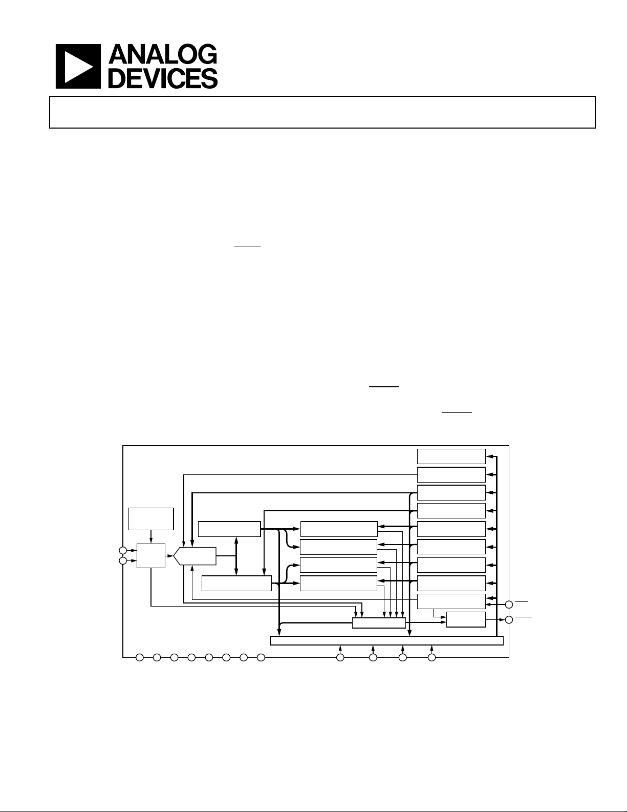
ON-CHIP
TEMPERATURE
1
Patents pending.
SENSOR
3
D+
ANALOG
MUX
4
D–
NC V
NC = NO CONNECT
BUSY RUN/STANDBY
EXTERNAL DIODE OPEN-CIRCUIT
1 2 5 7 8 9 13 16 12 14 10 6
DD
LOCAL TEMPERATURE
VALUE REGISTER
A-TO-D
CONVERTER
REMOTE TEMPERATURE
VALUE REGISTERS
ADM1023
GNDNC GND NC NC NC SDATA SCLK ADD0 ADD1
FUNCTIONAL BLOCK DIAGRAM
GENERAL DESCRIPTION
The ADM10231 is a 2-channel digital thermometer and
under/over temperature alarm for use in personal computers
and other systems requiring thermal monitoring and management. Optimized for the Pentium® III; the higher accuracy
allows systems designers to safely reduce temperature guard
banding and increase system performance. The device can
measure the temperature of a microprocessor using a diodeconnected PNP transistor, which may be provided on-chip in
the case of the Pentium III or similar processors, or can be a
low-cost, discrete NPN/PNP device such as the 2N3904/2N3906.
A novel measurement technique cancels out the absolute value
of the transistor’s base emitter voltage so that no calibration is
required. The second measurement channel measures the
output of an on-chip temperature sensor to monitor the
temperature of the device and its environment.
The ADM1023 communicates over a 2-wire serial interface
compatible with SMBus standards. Under- and overtemperature
limits can be programmed into the device over the serial bus,
and an
temperature is out of range. This output can be used as an
interrupt, or as an SMBus
LOCAL TEMPERATURE
LOW-LIMIT COMPARATOR
LOCAL TEMPERATURE
HIGH-LIMIT COMPARATOR
REMOTE TEMPERATURE
LOW-LIMIT COMPARATOR
REMOTE TEMPERATURE
HIGH-LIMIT COMPARATOR
STATUS REGISTER
SMBus INTERFACE
Figure 1.
ALERT
output signals when the on-chip or remote
ALERT
.
ADDRESS POINTER
REGISTER
ONE-SHOT
REGISTER
CONVERSION RATE
REGISTER
OFFSET
REGISTERS
LOCAL TEMPERATURE
LOW-LIMIT REGISTER
LOCAL TEMPERATURE
HIGH-LIMIT REGISTER
REMOTE TEMPERATURE
LOW-LIMIT REGISTERS
REMOTE TEMPERATURE
HIGH-LIMIT REGISTERS
CONFIGURATION
REGISTER
INTERRUPT
MASKING
ADM1023
15
STBY
11
ALERT
00058-001
Rev. G
Information furnished by Analog Devices is believed to be accurate and reliable.
However, no responsibility is assumed by Analog Devices for its use, nor for any
infringements of patents or other rights of third parties that may result from its use.
Specifications subject to change without notice. No license is granted by implication
or otherwise under any patent or patent rights of Analog Devices. Trademarks and
registered trademarks are the property of their respective owners.
One Technology Way, P.O. Box 9106, Norwood, MA 02062-9106, U.S.A.
Tel: 781.329.4700
Fax: 781.326.8703 © 2005 Analog Devices, Inc. All rights reserved.
www.analog.com
Page 2

ADM1023
TABLE OF CONTENTS
Specifications..................................................................................... 3
Serial Bus Interface..................................................................... 12
Absolute Maximum Ratings............................................................ 4
ESD Caution.................................................................................. 4
Pin Configuration and Functional Description ........................... 5
Typical Performance Characteristics ............................................. 6
Theory of Operation ........................................................................ 8
Functional Description................................................................ 8
Measurement Method.................................................................. 9
Sources of Errors on Thermal Transistors Measurement
Method........................................................................................... 9
Temperature Data Format......................................................... 10
Register Functions...................................................................... 10
REVISION HISTORY
2/05—Rev. F to Rev. G
Updated Format.................................................................. Universal
Changes to Specifications.................................................................3
Changes to Absolute Maximum Ratings........................................4
Changes to Figure 14.........................................................................8
Changes to Figure 21.......................................................................17
Changes to Ordering Guide...........................................................18
4/03—Rev. E to Rev. F
Added Reference to Figure 1............................................................2
4/03—Rev. D to Rev. E
Added ESD Caution..........................................................................3
Updated Outline Dimensions........................................................13
Address Pins................................................................................ 12
ALERT
Output............................................................................ 14
Low Power Standby Modes....................................................... 15
Sensor Fault Detection .............................................................. 15
Applications..................................................................................... 16
Factors Affecting Accuracy....................................................... 16
Layout Considerations............................................................... 16
Application Circuits................................................................... 17
Outline Dimensions....................................................................... 18
Ordering Guide .......................................................................... 18
9/02—Rev. C to Rev. D
Outline Dimensions updated...........................................................13
5/02—Rev. B to Rev. C
Figures 2 to 11 changed to TPCs 1–10, renumbered figures
accordingly ......................................................................................... 4
Text change to Figure 9 (TPC 8)......................................................5
Callouts in text added for Tables IV–VI......................................... 8
Change to Serial Bus Interface section ...........................................9
4/00—Revision 0: Initial Version
Rev. G | Page 2 of 20
Page 3

ADM1023
SPECIFICATIONS
TA = T
MIN
to T
Table 1.
Parameter Min Typ Max Unit Test Conditions/Comments
POWER SUPPLY AND ADC
Temperature Resolution, Local Sensor 1 °C Guaranteed no missed codes
Temperature Resolution, Remote Sensor 0.125 °C Guaranteed no missed codes
Temperature Error, Local Sensor −1.5 ±0.5 +1.5 °C TA = 60°C to 100°C
−3 ±1 +3 °C TA = 0°C to 120°C
Temperature Error, Remote Sensor −1 +1 °C TA, TD = 60°C to 100°C2
−3 +3 °C TA, TD = 0°C to 120°C2
Relative Accuracy 0.25 °C TA = 60°C to 100°C
Supply Voltage Range3 3 3.6 V
Undervoltage Lockout Threshold 2.55 2.7 2.8 V VDD input, disables ADC, rising edge
Undervoltage Lockout Hysteresis 25 mV
Power-On Reset Threshold 0.9 1.7 2.2 V VDD, falling edge4
POR Threshold Hysteresis 50 mV
Standby Supply Current 1 5 µA VDD = 3.3 V, no SMBus activity
4 µA SCLK at 10 kHz
Average Operating Supply Current 130 200 µA 0.25 conversions/sec rate
Autoconvert Mode, Averaged Over 4 Sec 225 330 µA 2 conversions/sec rate
Conversion Time 65 115 170 ms
Remote Sensor Source Current 120 205 300 µA High level4
7 12 16 µA Low level4
D-Source Voltage 0.7 V
Address Pin Bias Current (ADD0, ADD1) 50 µA Momentary at power-on reset
SMBus INTERFACE (See Figure 3)
Logic Input High Voltage, VIH 2.2 V VDD = 3 V to 5.5 V
STBY, SCLK, SDATA
Logic Input Low Voltage, VIL 0.8 V VDD = 3 V to 5.5 V
STBY, SCLK, SDATA
SMBus Output Low Sink Current 6 mA SDATA forced to 0.6 V
ALERT
Output Low Sink Current
Logic Input Current, IIH, IIL −1 +1 µA
SMBus Input Capacitance, SCLK, SDATA 5 pF
SMBus Clock Frequency 400 kHz
SMBus Clock Low Time, t
SMBus Clock High Time, t
SMBus Start Condition Setup Time, t
SMBus Start Condition Hold Time, t
SMBus Stop Condition Setup Time, t
SMBus Data Valid to SCLK Rising Edge Time, t
SMBus Bus Free Time, t
SCLK SDATA Rise Time, t
SCLK SDATA Fall Time, t
1
T
= 120°C, T
MAX
2
TD is temperature of remote thermal diode; TA, TD = 60°C to 100°C.
3
Operation at VDD = 5 V guaranteed by design; not production tested.
4
Guranteed by design, not production tested.
1
, VDD = 3.0 V to 3.6 V, unless otherwise noted.
MAX
1.3 µs t
LOW
0.6 µs t
HIGH
0.6 µs
SU:STA
0.6 µs Time from 10% of SDATA to 90% of SCLK
HD:STA
0.6 µs Time from 90% of SCLK to 10% of SDATA
SU:STO
100 ns Time for 10% or 90% of SDATA to 10% of SCLK
SU:DAT
1.3 µs Between start/stop condition
BUF°
300 ns Master clocking in data
R MAX
300 ns VDD = 0 V
F MAX
= 0°C.
MIN
From stop bit to conversion complete (both
channels) D+ forced to D− + 0.65 V
1 mA
ALERT
forced to 0.4 V
between 10% points
LOW
between 90% points
HIGH
Rev. G | Page 3 of 20
Page 4

ADM1023
ABSOLUTE MAXIMUM RATINGS
Table 2.
Parameters Ratings
Positive Supply Voltage (VDD) to GND −0.3 V to +6 V
D+, ADD0, ADD1 −0.3 V to VDD + 0.3 V
D− to GND −0.3 V to +0.6 V
SCLK, SDATA,
Input Current ±50 mA
Input Current, D− ±1 mA
ESD Rating, All Pins (Human Body Model) 2000 V
Continuous Power Dissipation
Up to 70°C 650 mW
Derating Above 70°C 6.7 mW/°C
Operating Temperature Range −55°C to +125°C
Maximum Junction Temperature (T
Storage Temperature Range −65°C to +150°C
Lead Temperature (Soldering 10 sec) 300°C
IR Reflow Peak Temperature 220°C
IR Reflow Peak Temperature for Pb-Free 260°C
ALERT, STBY
J MAX
−0.3 V to +6 V
) 150°C
Stresses above those listed under Absolute Maximum Ratings
may cause permanent damage to the device. This is a stress
rating only; functional operation of the device at these or any
other conditions above those indicated in the operational
section of this specification is not implied. Exposure to absolute
maximum rating conditions for extended periods may affect
device reliability.
THERMAL CHARACTERISTICS
16-lead QSOP package:
θ
= 105°C/W
JA
= 39°C/W
θ
JC
ESD CAUTION
ESD (electrostatic discharge) sensitive device. Electrostatic charges as high as 4000 V readily accumulate
on the human body and test equipment and can discharge without detection. Although this product
features proprietary ESD protection circuitry, permanent damage may occur on devices subjected to
high energy electrostatic discharges. Therefore, proper ESD precautions are recommended to avoid
performance degradation or loss of functionality.
Rev. G | Page 4 of 20
Page 5
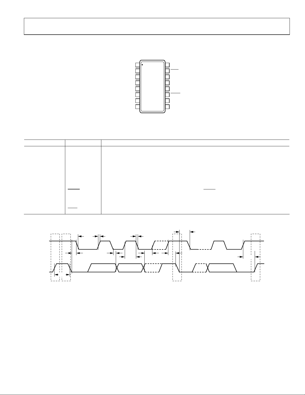
ADM1023
A
PIN CONFIGURATION AND FUNCTION DESCRIPTION
1
NC
2
V
DD
3
D+
ADM1023
4
D–
TOP VIEW
(Not to Scale)
5
NC
6
DD1
7
GND
8
GND NC
NC = NO CONNECT
Figure 2. Pin Configuration
16
15
14
13
12
11
10
9
NC
STBY
SCLK
NC
SDATA
ALERT
ADD0
00058-002
Table 3. Pin Function Description
Pin No. Mnemonic Description
1, 5, 9, 13, 16 NC No Connect.
2 VDD Positive Supply, 3 V to 5.5 V.
3 D+ Positive Connection to Remote Temperature Sensor.
4 D− Negative Connection to Remote Temperature Sensor.
6 ADD1 Three-State Logic Input, Higher Bit of Device Address.
7, 8 GND Supply 0 V Connection.
10 ADD0 Three-State Logic Input, Lower Bit of Device Address.
11
ALERT
Open-Drain Logic Output Used as Interrupt or SMBus
ALERT
12 SDATA Logic Input/Output, SMBus Serial Data. Open-drain output.
14 SCLK Logic Input, SMBus Serial Clock.
15
STBY
Logic Input Selecting Normal Operation (High) or Standby Mode (Low).
.
SCL
SDA
t
t
HD;DAT
t
R
t
HIGH
t
F
t
SU;DAT
t
LOW
t
HD;STA
t
BUF
P
S
Figure 3. Diagram for Serial Bus Timing
t
SU;STA
HD;STA
t
SU;STO
PS
00058-003
Rev. G | Page 5 of 20
Page 6
ADM1023
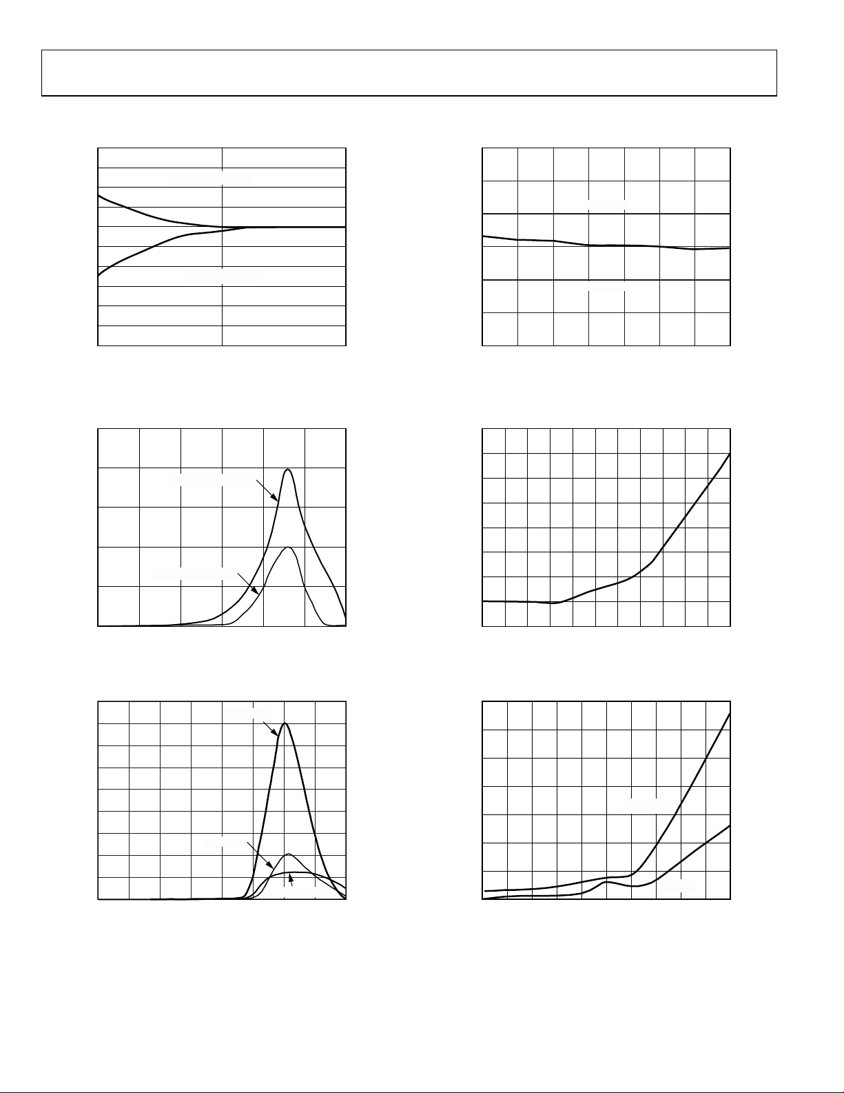
TYPICAL PERFORMANCE CHARACTERISTICS
20
15
10
5
0
–5
–10
–15
TEMPERATURE ERROR (°C)
–20
–25
–30
Figure 4. Temperature Error vs. Resistance from Track to V
D+ TO GND
D+ TO V
DD
LEAKAGE RESISTANCE (MΩ)
100110
and GND
DD
00058-004
3
2
1
0
–1
TEMPERATURE ERROR (°C)
–2
–3
UPPER SPEC LEVEL
LOWER SPEC LEVEL
12050 60 70 80 90 100 110
TEMPERATURE (°C)
Figure 7. Temperature Error of ADM1023 vs. Pentium III Temperature
00058-007
5
4
3
2
TEMPERATURE ERROR (°C)
1
0
250mV p-p REMOTE
100mV p-p REMOTE
FREQUENCY (Hz)
Figure 5. Remote Temperature Error vs. Supply Noise Frequency
9
8
7
6
5
4
3
2
TEMPERATURE ERROR (°C)
1
0
100mV p-p
50mV p-p
25mV p-p
FREQUENCY (Hz)
Figure 6. Temperature Error vs. Common-Mode Noise Frequency
14
12
10
8
6
4
2
TEMPERATURE ERROR (°C)
0
100M100 1k 10k 100k 1M 10M
00058-005
–1
CAPACITANCE (nF)
24246810121416182022
00058-008
Figure 8. Temperature Error vs. Capacitance Between D+ and D−
70
60
50
40
30
20
SUPPLY CURRENT (µA)
10
100M1 10 100 1k 10k 100k 1M 10M
00058-006
0
SCLK FREQUENCY (kHz)
VDD = 3.3V
VDD = 5V
10001 5 10 25 50 75 100 250 500 750
00058-009
Figure 9. Standby Supply Current vs. SCLK Frequency
Rev. G | Page 6 of 20
Page 7

ADM1023
4
3
10mV p-p
2
1
TEMPERATURE ERROR (°C)
100
80
60
40
20
SUPPLY CURRENT (µA)
0
0
FREQUENCY (Hz)
1G100k 1M 10M 100M
Figure 10. Temperature Error vs. Differential-Mode Noise Frequency
550
500
450
400
350
300
250
200
SUPPLY CURRENT (µA)
150
100
50
CONVERSION RATE (Hz)
3.3 V
5 V
8.00000.0625 0.1250 0.2500 0.5000 1.0000 2.0000 4.0000
Figure 11. Operating Supply Current vs. Conversion Rate, VDD = 5 V and 3.3 V
00058-010
00058-011
–20
SUPPLY VOLTAGE (V)
Figure 12. Standby Supply Current vs. Supply Voltage
125
100
75
50
TEMPERATURE (°C)
25
0
REMOTE
TEMPERATURE
TIME (Seconds)
INT
TEMPERATURE
Figure 13. Response to Thermal Shock
5.00 0.5 1.0 1.5 2.0 2.5 3.0 3.5 4.0 4.5
00058-012
100123456789
00058-013
Rev. G | Page 7 of 20
Page 8

ADM1023
THEORY OF OPERATION
FUNCTIONAL DESCRIPTION
The ADM1023 contains a 2-channel A-to-D converter (ADC)
with special input-signal conditioning to enable operation with
remote and on-chip diode temperature sensors. When the
ADM1023 is operating normally, the ADC operates in a freerunning mode. The analog input multiplexer alternately selects
either the on-chip temperature sensor to measure its local
temperature or the remote temperature sensor. These signals are
digitized by the ADC and the results are stored in the local and
remote temperature value registers. Only the eight most
significant bits (MSBs) of the local temperature value are stored
as an 8-bit binary word. The remote temperature value is stored
as an 11-bit binary word in two registers. The eight MSBs are
stored in the remote temperature value high byte register at
Address 0x01. The three least significant bits (LSBs) are stored,
left justified, in the remote temperature value low byte register
at Address 0x10.
Error sources such as PCB track resistance and clock noise can
introduce offset errors into measurements on the remote
channel. To achieve the specified accuracy on this channel,
these offsets must be removed, and two offset registers are
provided for this purpose at Address 0x11 and Address 0x12.
An offset value may automatically be added to, or subtracted
from, the measurement by writing an 11-bit, twos complement
value to Register 0x11 (high byte) and Register 0x12 (low byte,
left justified).
The offset registers default to zero at power-up and will have no
effect if nothing is written to them.
The measurement results are compared with local and remote,
high and low temperature limits, stored in six on-chip limit
registers. As with the measured value, the local temperature
limits are stored as 8-bit values and the remote temperature
limits as 11-bit values. Out-of-limit comparisons generate flags
that are stored in the status register, and one or more out-of-
ALERT
limit results cause the
output to pull low.
Registers can be programmed, and the device controlled and
configured, via the serial system management bus (SMBus).
The contents of any register can also be read back via the
SMBus.
Control and configuration functions consist of:
• Switching the device between normal operation and
standby mode.
ALERT
• Masking or enabling the
output.
• Selecting the conversion rate.
On initial power-up, the remote and local temperature values
default to −128°C. The device normally powers up converting,
making a measure of local and remote temperature. These
values are then stored before making a comparison with the
stored limits. However, if the part is powered up in standby
STBY
mode (
pin pulled low), no new values are written to the
register before a comparison is made. As a result, both RLOW
and LLOW are tripped in the status register, thus generating an
ALERT
output. This may be cleared in one of two ways:
• Change both the local and remote lower limits to –128°C
and read the status register (which in turn clears the
ALERT
output).
• Take the part out of standby and read the status register
ALERT
(which in turn clears the
output). This works only
when the measured values are within the limit values.
REMOTE
SENSING
TRANSISTOR
V
= 65kHz
C
DD
IN× I
D+
1
C1
D–
1
CAPACITOR C1 IS OPTIONAL. IT IS ONLY NECESSARY IN NOISY ENVIRONMENTS.
C1 = 1000pF MAX.
Figure 14. Input Signal Conditioning
I
BIAS
BIAS
DIODE
Rev. G | Page 8 of 20
LOW-PASS FILTER
f
V
OUT+
TO ADC
V
OUT–
00058-014
Page 9

ADM1023
MEASUREMENT METHOD
A simple method of measuring temperature is to exploit the
negative temperature coefficient of a diode, or the base emitter
voltage of a transistor, operating at constant current. Thus, the
temperature may be obtained from a direct measurement of V
where
()
V 1×=
BE
nKT
q
I
C
(1)
n
I
S
This technique, however, requires calibration to nullify the
effect of the absolute value of V
, which varies from device to
BE
device.
The technique used in the ADM1023 is to measure the change
when the device is operated at two different collector
in V
BE
currents.
This is given by
nKT
V
BE
q
(2)
()
Nn
1×=∆
where:
K is Boltzmann’s constant.
–19
q is the charge on the electron (1.6 × 10
Coulombs).
T is the absolute temperature in Kelvins.
N is the ratio of the two collector currents.
n is the ideality factor of the thermal diode (TD).
To me as u re Δ V
, the sensor is switched between operating
BE
currents of I and NI. The resulting waveform is passed through
a low-pass filter to remove noise, then to a chopper-stabilized
amplifier that performs the functions of amplification and
rectification of the waveform to produce a dc voltage
proportional to ΔV
. This voltage is measured by the ADC,
BE
which gives a temperature output in binary format. To further
reduce the effects of noise, digital filtering is performed by
averaging the results of 16 measurement cycles. Signal
conditioning and measurement of the internal temperature
sensor is performed in a similar manner.
Figure 14 shows the input signal conditioning used to measure
the output of an external temperature sensor. This figure shows
the external sensor as a substrate PNP transistor, provided for
temperature monitoring on some microprocessors, but it could
equally well be a discrete transistor. If a discrete transistor is
used, the collector will not be grounded and should be linked to
the base. To prevent ground noise from interfering with the
measurement, the more negative terminal of the sensor is not
referenced to ground, but is biased above ground by an internal
diode at the D− input. If the sensor is operating in a noisy
environment, C1 may optionally be added as a noise filter. Its
BE
value is 1000 pF maximum. See the Layout Considerations
section for more information on C1.
SOURCES OF ERRORS ON THERMAL TRANSISTORS MEASUREMENT METHOD
THE EFFECT OF IDEALITY FACTOR (n)
The effects of ideality factor (n) and beta (β) of the temperature
measured by a thermal transistor are described in this section.
For a thermal transistor implemented on a submicron process,
such as the substrate PNP used on a Pentium III processor, the
temperature errors due to the combined effect of the ideality
factor and beta are shown to be less than 3°C. Equation 2 is
optimized for a substrate PNP transistor (used as a thermal
diode) usually found on CPUs designed on submicron CMOS
processes such as the Pentium III processor. There is a thermal
diode on board each of these processors. The n in Equation 2
represents the ideality factor of this thermal diode. This ideality
factor is a measure of the deviation of the thermal diode from
ideal behavior.
According to Pentium III processor manufacturing specifications,
measured values of n at 100°C are
TD
0125.1008.10057.1 =<=<=
−=+×
+=+×
nnn
MAXTYPICALMIN
The ADM1023 takes this ideality factor into consideration
when calculating temperature T
ADM1023 is optimized for n
of the thermal diode. The
TD
= 1.008; any deviation on n
TYPICAL
from this typical value causes a temperature error that is
calculated below for the n
MIN
= 100°C.
TD
=∆ CKelvinT
−
008.1
processor at T
MIN
008.10057.1
and n
of a Pentium III
MAX
()
−
008.10125.1
MAX
=∆ CKelvinT
008.1
()
Thus, the temperature error due to variation on n of the
thermal diode for a Pentium III processor is about 2.5°C.
In general, this additional temperature error of the thermal
diode measurement due to deviations on n from its typical
value is given by
008.1
n
−
T +×
=∆ 15.273
008.1
where T
is in °C.
TD
()
TKelvin
Beta of Thermal Transistor (β)
In Figure 14, the thermal diode is a substrate PNP transistor
where the emitter current is forced into the device. The
derivation of Equation 2 assumed that the collector currents
were scaled by N as the emitter currents were also scaled by N.
Thus, this assumes that beta (β) of the transistor is constant for
oo
C85.010015.273
oo
C67.110015.273
Rev. G | Page 9 of 20
Page 10

ADM1023
various collector currents. Figure 15 shows typical β variation
vs. collector current for Pentium III processors at 100°C. The
maximum β is 4.5, and varies less than 1% over the collector
current range from 7 µA to 300 µA.
< 4.5
β
MAX
∆β
β
7 300
Figure 15. Variation of β with Collector Currents
I
(mA)
C
I
= I
C
β
β+1
Expressing the collector current in terms of the emitter current
= IE [β/(β + 1)]
I
C
where β(300 µA) = β(7 µA)(1 + ε ), ε = Δβ/β and β = β(7 µA).
Rewriting the equation for ΔV
, to include the ideality factor,
BE
n, and beta, β, we have
⎡
nKT
V
BE
q
()( )
×=∆ Nn
l
⎢
()
⎣
+×+
βε
++
βε
⎤
11
(3)
×
⎥
11
⎦
β variations of less than 1% (ε < 0.01) contribute to temperature
errors of less than 0.4°C.
TEMPERATURE DATA FORMAT
One LSB of the ADC corresponds to 0.125°C, so the ADM1023
can measure from 0°C to 127.875°C. The temperature data
format and extended temperature resolution are shown in
Table 4 and Table 5.
Table 4. Temperature Data Format
(Local Temperature and Remote Temperature High Byte)
Temperature °(C)
0 0 000 0000
1 0 000 0001
10 0 000 1010
25 0 001 1001
50 0 011 0010
75 0 100 1011
100 0 110 0100
125 0 111 1101
127 0 111 1111
1
The ADM1023 differs from the ADM1021 in that the temperature resolution
of the remote channel is improved from 1°C to 0.125°C, but it cannot
measure temperatures below 0°C. If negative temperature measurement is
required, the ADM1021 should be used.
The results of the local and remote temperature measurements
are stored in the local and remote temperature value registers
and are compared with limits programmed into the local and
remote high and low limit registers.
1
Digital Output
I
E
E
00058-015
Table 5. Extended Temperature Resolution
(Remote Temperature Low Byte)
Extended Resolution (°C) Remote Temperature Low Byte
0.000 0000 0000
0.125 0010 0000
0.250 0100 0000
0.375 0110 0000
0.500 1000 0000
0.625 1010 0000
0.750 1100 0000
0.875 1110 0000
REGISTER FUNCTIONS
The ADM1023 contains registers that are used to store the
results of remote and local temperature measurements, high
and low temperature limits, and to configure and control the
device. A description of these registers follows, and further
details are given in Table 6 to Table 10. Most of the registers for
the ADM1023 are dual port and have different addresses for
read and write operations. Attempting to write to a read
address, or to read from a write address, produces an invalid
result. Register addresses above 0x14 are reserved for future use
or factory test purposes and should not be written to.
Address Pointer Register
The address pointer register does not have, nor does it require,
an address because it is the register to which the first data byte
of every write operation is automatically written. This data byte
is an address pointer that sets up one of the other registers for
the second byte of the write operation, or for a subsequent read
operation.
Value Registers
The ADM1023 has three registers to store the results of local
and remote temperature measurements. These registers are
written to by the ADC and can only be read over the SMBus.
The Offset Register
Two offset registers are provided at Address 0x11 and
Address 0x12. These are provided so that the user may remove
errors from the measured values of remote temperature. These
errors may be introduced by clock noise and PCB track
resistance. See Table 7 for an example of offset values.
The offset value is stored as an 11-bit, twos complement value
in Register 0x11 (high byte) and Register 0x12 (low byte, left
justified). The value of the offset is negative if the MSB of
Register 0x11 is 1, and is positive if the MSB of Register 0x11 is
0. This value is added to the remote temperature. These
registers default to zero at power-up and will have no effect if
nothing is written to them. The offset register can accept values
from −128.875°C to +127.875°C. The ADM1023 detects
overflow so the remote temperature value register will not wrap
around +127°C or −128°C.
Rev. G | Page 10 of 20
Page 11

ADM1023
Table 6. List of ADM1023 Registers
Read Address (Hex) Write Address (Hex) Name Power-On Default
Not applicable Not applicable Address pointer Undefined
00 Not applicable Local temperature value 1000 0000 (0x80) (−128°C)
01 Not applicable Remote temperature value high byte 1000 0000 (0x80) (−128°C)
02 Not applicable Status Undefined
03 09 Configuration 0000 0000 (0x00)
04 0A Conversion rate 0000 0010 (0x02)
05 0B Local temperature high limit 0111 1111 (0x7F) (+127°C)
06 0C Local temperature low limit 1100 1001 (0xC9) (−55°C)
07 0D Remote temperature high limit high byte 0111 1111 (0x7F) (+127°C)
08 0E Remote temperature low limit high byte 1100 1001 (0xC9) (−55°C)
Not applicable 0F
10 Not applicable Remote temperature value low byte 0000 0000
11 11 Remote temperature offset high byte 0000 0000
12 12 Remote temperature offset low byte 0000 0000
13 13 Remote temperature high limit low byte 0000 0000
14 14 Remote temperature low limit low byte 0000 0000
19 Not applicable Reserved 0000 0000
20 21 Reserved Undefined
FE Not applicable Manufacturer device ID 0100 0001 (0x41)
FF Not applicable Die revision code 0011 xxxx (0x3x)
1
Writing to Address 0F causes the ADM1023 to perform a single measurement. It is not a data register as such, thus, it does not matter what data is written to it.
1
One-shot
Table 7. Offset Values
Remote Remote
Temperature Temperature
Offset Registers Offset (Including (Without
0x11 0x12 Value Offset) Offset)
1111 1100 0000 0000 −4°C 14°C 18°C
1111 1111 0000 0000 −1°C 17°C 18°C
1111 1111 1110 0000 −0.125°C 17.875°C 18°C
0000 0000 0000 0000 0°C 18°C 18°C
0000 0000 0010 0000 +0.125°C 18.125°C 18°C
0000 0001 0000 0000 +1°C 19°C 18°C
0000 0100 0000 0000 +4°C 22°C 18°C
Status Register
Bit 7 of the status register (see Table 8) indicates that the ADC is
busy converting when it is high. Bit 6 to Bit 3 are flags
indicating the results of the limit comparisons.
If the local and/or remote temperature measurement is above
the corresponding high temperature limit, or below the
corresponding low temperature limit, one or more of these flags
will be set. Bit 2 is a flag that is set if the remote temperature
sensor is open-circuit. These five flags are NOR’d together, so
that if any of them are high, the
set and the
output will go low. Reading the status
ALERT
interrupt latch will be
ALERT
of-limit measurement, or the sensor is open-circuit, the
corresponding flag bit cannot be reset. A flag bit can only be
reset if the corresponding value register contains an in-limit
measurement, or the sensor is good.
The
register, but resets when the
by the master reading the device address, provided the error
condition has gone away and the status register flag bits have
been reset.
Table 8. Status Register Bit Assignments
Bit Name Function
7 BUSY At 1 when ADC converting.
6 LHIGH
5 LLOW
4 RHIGH
3 RLOW
2 OPEN
1 to 0 Reserved.
1
register clears the five flag bits, provided the error conditions
that caused the flags to be set have gone away. While a limit
comparator is tripped due to a value register containing an out-
ALERT
interrupt latch is not reset by reading the status
output has been serviced
ALERT
1
At 1 when local high temp limit tripped.
1
At 1 when local low temp limit tripped.
1
At 1 when remote high temp limit tripped.
1
At 1 when remote low temp limit tripped.
1
At 1 when remote sensor open-circuit.
These flags stay high until the status register is read or they are reset by POR.
Rev. G | Page 11 of 20
Page 12

ADM1023
Configuration Register
Two bits of the configuration register are used. If Bit 6 is 0,
which is the power-on default, the device is in operating mode
with the ADC converting (see Table 9). If Bit 6 is set to 1, the
device is in standby mode and the ADC does not convert.
output is
0
= 3.3 V
CC
STBY
pin low.
ALERT
ALERT
Standby mode can also be selected by taking the
In standby mode, the values of remote and local temperature
remain at the value they were before the part was placed in
standby.
Bit 7 of the configuration register is used to mask the
output. If Bit 7 is 0, which is the power-on default, the
output is enabled. If Bit 7 is set to 1, the
ALERT
disabled.
Table 9. Configuration Register Bit Assignments
Bit Name Function Power-On Default
7 MASK1
6
1 = Standby
5 to 0 Reserved 0
RUN
/STOP
ALERT Enabled
0 =
ALERT
1 =
0 = Run 0
Masked
Conversion Rate Register
The lowest three bits of this register are used to program the
conversion rate by dividing the ADC clock by 1, 2, 4, 8, 16, 32,
64, or 128, to give conversion times from 125 ms (Code 0x07)
to 16 seconds (Code 0x00). This register can be written to and
read back over the SMBus. The higher five bits of this register
are unused and must be set to zero. Use of slower conversion
times greatly reduces the device’s power consumption, as shown
in Table 10.
Table 10. Conversion Rate Register Code
Average Supply Current
Data Conversion/Sec
0x00 0.0625 150
0x01 0.125 150
0x02 0.25 150
0x03 0.5 150
0x04 1 150
0x05 2 150
0x06 4 160
0x07 8 180
0x08 to
0xFF
Reserved
µA Typ at V
Limit Registers
The ADM1023 has six limit registers to store local and remote,
high and low temperature limits. These registers can be written
to, and read back over, the SMBus. The high limit registers
perform a > comparison, while the low limit registers perform a
< comparison. For example, if the high limit register is programmed
as a limit of 80°C, measuring 81°C will result in an alarm condition. Even though the temperature range is 0 to 127°C, it is
possible to program the limit register with negative values. This
is for backwards-compatibility with the ADM1021.
One-Shot Register
The one-shot register is used to initiate a single conversion and
comparison cycle when the ADM1023 is in standby mode, after
which the device returns to standby. This is not a data register
as such, and it is the write operation that causes the one-shot
conversion. The data written to this address is irrelevant and is
not stored.
SERIAL BUS INTERFACE
Control of the ADM1023 is carried out via the serial bus. The
ADM1023 is connected to this bus as a slave device, under the
control of a master device. Note that the SMBus SDA and SCLK
pins are three-stated when the ADM1023 is powered down and
will not pull down the SMBus.
ADDRESS PINS
In general, every SMBus device has a 7-bit device address
(except for some devices that have extended, 10-bit addresses).
When the master device sends a device address over the bus,
the slave device with that address responds. The ADM1023 has
two address pins, ADD0 and ADD1, to allow selection of the
device address, so that several ADM1023s can be used on the
same bus and to avoid conflict with other devices. Although
only two address pins are provided, these pins are three-state
and can be grounded, left unconnected, or tied to V
total of nine different addresses are possible, as shown in Table 11.
Note that the state of the address pins is only sampled at powerup, so changing them after power-up will have no effect.
1
Table 11. Device Addresses
ADD0 ADD1 Device Address
0 0 0011 000
0 NC 0011 001
0 1 0011 010
NC 0 0101 001
NC NC 0101 010
NC 1 0101 011
1 0 1001 100
1 NC 1001 101
1 1 1001 110
1
ADD0, ADD1 sampled at power-up only.
, so that a
DD
Rev. G | Page 12 of 20
Page 13

ADM1023
A
S
A
The serial bus protocol operates as follows:
1. The master initiates data transfer by establishing a start
condition, defined as a high-to-low transition on the serial
data line, SDATA, while the serial clock line, SCLK, remains
high. This indicates that an address/data stream will follow.
All slave peripherals connected to the serial bus respond to
the start condition and shift in the next 8 bits. These bits
W
consist of a 7-bit address (MSB first) plus an R/
bit, which
determines the direction of the data transfer, that is, whether
data will be written to, or read from, the slave device.
The peripheral whose address corresponds to the transmitted
address responds by pulling the data line low during the low
period before the ninth clock pulse, known as the
Acknowledge bit. All other devices on the bus remain idle
while the selected device waits for data to be read from or
written to it. If the R/
device. If the R/
bit is 0, the master writes to the slave
W
bit is 1, the master reads from the slave
W
device.
191
SCLK
2. Data is sent over the serial bus in sequences of nine clock
pulses, 8 bits of data followed by an Acknowledge bit from
the slave device. Transitions on the data line must occur
during the low period of the clock signal and remain stable
during the high period because a low-to-high transition
when the clock is high may be interpreted as a stop signal.
The number of data bytes that can be transmitted over the
serial bus in a single read or write operation is limited only by
what the master and slave devices can handle.
3. When all data bytes have been read or written, stop
conditions are established. In write mode, the master pulls
the data line high during the 10th clock pulse to assert a stop
condition. In read mode, the master device overrides the
Acknowledge bit by pulling the data line high during the low
period before the ninth clock pulse. This is known as No
Acknowledge. The master will then take the data line low
during the low period before the 10th clock pulse, then high
during the 10th clock pulse to assert a stop condition.
9
SDAT
START BY
MASTER
0
10
1
FRAME 1
SERIAL BUS ADDRESS BYTE
SCLK (CONTINUED)
SDATA (CONTINUED)
1
A0
A1
R/W
ACK. BY
ADM1023
1
D7
D6
D7
D5
D6
D4
D5
ADDRESS POINTER REGISTER BYTE
D4
D3
FRAME 3
DATA BYTE
Figure 16. Writing a Register Address to the Address Pointer Register, then Writing Data to the Selected Register
D3
FRAME 2
D2
D2
D1
D0
ACK. BY
ADM1023
9
D1
D0
ACK. BY
ADM1023
STOP BY
MASTER
00058-016
D0
9
ACK. BY
ADM1023
STOP BY
MASTER
00058-017
SCLK
DAT
START BY
MASTER
19
0
10
SERIAL BUS ADDRESS BYTE
1
FRAME 1
1
A0
A1
R/W
ADM1023
ACK. BY
1
D6
D7
D4
D5
ADDRESS POINTER REGISTER BYTE
D3
FRAME 2
D2
D1
Figure 17. Writing to the Address Pointer Register Only
Rev. G | Page 13 of 20
Page 14

ADM1023
SCLK
SDATA
START BY
MASTER
1
A5
A6
A3
A4
FRAME 1
SERIAL BUS ADDRESS BYTE
A1 A0
A2
Figure 18. Reading Data from a Previously Selected Register
R/W
Any number of bytes of data may be transferred over the serial
bus in one operation, but it is not possible to mix read and write
in one operation because the type of operation is determined at
the beginning and cannot subsequently be changed without
starting a new operation.
In the case of the ADM1023, write operations contain either
one or two bytes, while read operations contain one byte and
perform the following functions:
To write data to one of the device data registers, or read data
from it, the address pointer register must be set so that the
correct data register is addressed. Data can then be written into
that register or read from it. The first byte of a write operation
always contains a valid address that is stored in the address
pointer register. If data is to be written to the device, the write
operation contains a second data byte that is written to the
register selected by the address pointer register.
This is illustrated in Figure 16. The device address is sent over
the bus followed by R/
set to 0. This is followed by two data
W
bytes. The first data byte is the address of the internal data
register to be written to, which is stored in the address pointer
register. The second data byte is the data to be written to the
internal data register.
When reading data from a register there are two possibilities:
1. If the ADM1023’s address pointer register value is unknown,
or not the desired value, it is necessary to set it to the correct
value before data can be read from the desired data register.
This is done by performing a write to the ADM1023 as
before, but only the data byte containing the register read
address is sent, as data is not to be written to the register. This
is shown in Figure 17.
A read operation is then performed consisting of the serial
bus address, R/
bit set to 1, followed by the data byte read
W
from the data register. This is shown in Figure 18.
2. If the address pointer register is known to be at the desired
address already, data can be read from the corresponding
data register without first writing to the address pointer
register.
9
ACK. BY
ADM1023
1
D3
FRAME 2
D2
D1
D7
D6
D4
D5
DATA BYTE FROM ADM1023
9
D0
NO ACK.
BY MASTER
STOP BY
MASTER
00058-018
NOTES
• It is possible to read a data byte from a data register
without first writing to the address pointer register.
However, it is not possible to write data to a register
without writing to the address pointer register even if the
address pointer register is already at the correct value. This
is because the first data byte of a write is always written to
the address pointer register.
• Do not forget that ADM1023 registers have different
addresses for read and write operations. The write address
of a register must be written to the address pointer if data is
to be written to that register, but it is not possible to read
data from that address. The read address of a register must
be written to the address pointer before data can be read
from that register.
ALERT OUTPUT
ALERT
The
measurement is detected, or if the remote temperature sensor is
open-circuit. It is an open drain and requires a 10 kΩ pull-up to
. Several
V
DD
that the common line will go low if one or more of the
outputs goes low.
The
processor, or it may be used as an
the SMBus normally cannot signal to the master that they want
to talk, but the
One or more
SMBALERT
SMBALERT
procedure illustrated in Figure 19 occurs.
MASTER
RECEIVES
SMBALERT
START
output goes low whenever an out-of-limit
outputs can be wire-AND’ed together, so
ALERT
ALERT
output can be used as an interrupt signal to a
SMBALERT
SMBALERT
ALERT
function allows them to do so.
outputs are connected to a common
line connected to the master. When the
line is pulled low by one of the devices, the
ALERT RESPONSE
ADDRESS
MASTER SENDS
ARA AND READ
COMMAND
Figure 19. Use of
RD ACK
DEVICE
ADDRESS
DEVICE SENDS
ITS ADDRESS
SMBALERT
ALERT
. Slave devices on
NO
STOP
ACK
00058-019
Rev. G | Page 14 of 20
Page 15

ADM1023
SMBALERT
Step 1.
Step 2. Master initiates a read operation and sends the alert
Step 3. The device whose
Step 4. If more than one device’s
Step 5. Once the ADM1023 has responded to the ARA, it will
Process
SMBALERT
response address (ARA = 0001 100). This is a general
call address that must not be used as a specific device
address.
ARA and the master reads its device address. The
address of the device is now known and it can be
interrogated in the usual way.
with the lowest device address will have priority, in
accordance with normal SMBus arbitration.
reset its
condition that caused the
SMBALERT
again, and so on until all devices whose
were low have responded.
pulled low.
ALERT
output is low responds to the
ALERT
output is low, the one
output, provided that the error
ALERT
ALERT
no longer exists. If the
line remains low, the master will send ARA
ALERT
outputs
SENSOR FAULT DETECTION
The ADM1023 has a fault detector at the D+ input that detects
if the external sensor diode is open-circuit. This is a simple
voltage comparator that trips if the voltage at D+ exceeds
− 1 V (typical). The output of this comparator is checked
V
CC
when a conversion is initiated and sets Bit 2 of the status
register if a fault is detected.
If the remote sensor voltage falls below the normal measuring
range, for example, due to the diode being short-circuited, the
ADC will output –128°C (1000 0000 000). Since the normal
operating temperature range of the device only extends down to
0°C, this output code will never be seen in normal operation, so
it can be interpreted as a fault condition.
In this respect, the ADM1023 differs from, and improves upon,
competitive devices that output zero if the external sensor goes
short-circuit. Unlike the ADM1023, these other devices can
misinterpret a genuine 0°C measurement as a fault condition.
If the external diode channel is not being used and is shorted
ALERT
out, the resulting
(−128°C) to the low limit register.
may be cleared by writing 0x80
LOW POWER STANDBY MODES
The ADM1023 can be put into a low power standby mode using
STBY
hardware or software, that is, by taking the
by setting Bit 6 of the configuration register. When
high or Bit 6 is low, the ADM1023 operates normally. When
is pulled low or Bit 6 is high, the ADC is inhibited, and
STBY
any conversion in progress is terminated without writing the
result to the corresponding value register.
The SMBus is still enabled. Power consumption in the standby
mode is reduced to less than 10 µA if there is no SMBus activity,
or 100 µA if there are clock and data signals on the bus.
These two modes are similar but not identical. When
low, conversions are completely inhibited. When Bit 6 is set but
STBY
is high, a one-shot conversion of both channels can be
initiated by writing any data value to the one-shot register
(Address 0x0F).
input low, or
is
STBY
STBY
is
Rev. G | Page 15 of 20
Page 16

ADM1023
APPLICATIONS
FACTORS AFFECTING ACCURACY
Remote Sensing Diode
The ADM1023 is designed to work with substrate transistors
built into processors, or with discrete transistors. Substrate
transistors are generally PNP types with the collector connected
to the substrate. Discrete types can be either PNP or NPN,
connected as a diode (base-shorted to collector). If an NPN
transistor is used, then the collector and base are connected to
D+ and the emitter to D−. If a PNP transistor is used, the
collector and base are connected to D− and the emitter to D+.
LAYOUT CONSIDERATIONS
Digital boards can be electrically noisy environments, and the
ADM1023 is measuring very small voltages from the remote
sensor; therefore, care must be taken to minimize noise induced
at the sensor inputs. The following precautions are needed:
• Place the ADM1023 as close as possible to the remote
sensing diode. Provided that the worst noise sources, such as
clock generators, data/address buses, and CRTs are avoided,
this distance can be four to eight inches.
The user has no choice in the case of substrate transistors, but if
a discrete transistor is used, the best accuracy is achieved by
choosing devices according to the following criteria:
• Base emitter voltage greater than 0.25 V at 6 µA, at the
highest operating temperature.
• Base emitter voltage less than 0.95 V at 100 µA, at the lowest
operating temperature.
• Base resistance less than 100 Ω.
• Small variation in h
indicates tight control of V
(approximately 50 to 150), which
fe
characteristics.
BE
Transistors such as 2N3904, 2N3906, or equivalents in SOT-23
package are suitable devices to use.
Thermal Inertia and Self-Heating
Accuracy depends on the temperature of the remote-sensing
diode and/or the internal temperature sensor being at the same
temperature as that being measured; and a number of factors
can affect this. Ideally, the sensor should be in good thermal
contact with the part of the system being measured, such as the
processor, for example. If it is not, the thermal inertia caused by
the mass of the sensor will cause a lag in the response of the
sensor to a temperature change. In the case of the remote
sensor, this should not be a problem as it will be either a
substrate transistor in the processor, or a small package device
such as SOT-23 placed in close proximity to it.
The on-chip sensor, however, is often remote from the
processor and only monitors the general ambient temperature
around the package. The thermal time constant of the QSOP-16
package is about 10 seconds.
In practice, the package has electrical, and hence thermal,
connection to the printed circuit board; therefore, the
temperature rise due to self-heating is negligible.
• Route the D+ and D− tracks close together, in parallel, with
grounded guard tracks on each side. Provide a ground plane
under the tracks if possible (Figure 20).
• Use wide tracks to minimize inductance and reduce noise
pickup. 10 mil track minimum width and spacing is
recommended.
GND
D+
D–
GND
Figure 20. Arrangement of Signal Tracks
10MIL
10MIL
10MIL
10MIL
10MIL
10MIL
10MIL
00058-020
• Try to minimize the number of copper/solder joints, which
can cause thermocouple effects. Where copper/solder joints
are used, make sure that they are in both the D+ and D−
path and at the same temperature.
Thermocouple effects should not be a major problem as 1°C
corresponds to about 240 µV, and thermocouple voltages are
about 3 µV/°C of temperature difference. Unless there are
two thermocouples with a big temperature differential
between them, thermocouple voltages should be much less
than 240 µV.
• Place a 0.1 µF bypass capacitor close to the V
pin and
DD
1000 pF input filter capacitors across D+, D− close to the
ADM1023.
• If the distance to the remote sensor is more than eight inches,
the use of twisted pair cable is recommended. This is
effective up to approximately 6 to 12 feet.
• For longer distances (up to 100 feet), use shielded twisted
pair cable such as Belden #8451 microphone cable. Connect
the twisted pair to D+ and D−, and the shield to GND close
Rev. G | Page 16 of 20
Page 17

ADM1023
to the ADM1023. Leave the remote end of the shield
unconnected to avoid ground loops.
Because the measurement technique uses switched current
sources, excessive cable and/or filter capacitance can affect the
measurement. When using long cables, the filter capacitor may
be reduced or removed.
Cable resistance can also introduce errors. A 1 Ω series
resistance introduces about 1°C error.
APPLICATION CIRCUITS
Figure 21 shows a typical application circuit for the ADM1023,
using a discrete sensor transistor connected via a shielded,
3V
TO 5.5V
IN
I/O
OUT
ALERT
TO
CONTROL
CHIP
twisted pair cable. The pull-ups on SCLK, SDATA, and
are required only if they are not already provided elsewhere in
the system.
0.1µF
V
1000pF
SHIELD2N3904
ADM1023
D+
D–
GND
SCLK
SDATA
ALERT
ADD0
ADD1
DD
10kΩ 10kΩ
SET TO
REQUIRED
ADDRESS
10kΩ
The SCLK and SDATA pins of the ADM1023 can be interfaced
directly to the SMBus of an I/O chip. Figure 22 shows how the
ADM1023 might be integrated into a system using this type of
I/O controller.
D–
ADM1023
DISPLAY
DISPLAY
CACHE
HARD
CD ROM
2 IDE PORTS
USBUSB
2 USB PORTS
DISK
PROCESSOR
SYSTEM BUS
GMCH
ICH I/O
CONTROLLER
HUB
FWH
(FIRMWARE
HUB)
SYSTEM
MEMORY
PCI SLOTS
PCI BUS
SUPER I/O
D+
SCLK
SDATA
ALERT
SMBUS
Figure 22. System Using ADM1023 and I/O Controller
00058-022
00058-021
Figure 21. Typical Application Circuit
Rev. G | Page 17 of 20
Page 18

ADM1023
OUTLINE DIMENSIONS
0.193
BSC
0.012
0.008
9
8
0.154
BSC
0.069
0.053
SEATING
PLANE
0.236
BSC
0.010
0.006
8°
0°
0.050
0.016
0.065
0.049
0.010
0.004
COPLANARITY
0.004
Figure 23. 16-Lead Shrink Small Outline Package [QSOP]
16
1
PIN 1
0.025
BSC
COMPLIANT TO JEDEC STANDARDS MO-137AB
(RQ-16)
Dimensions shown in inches
ORDERING GUIDE
Model Temperature Range Package Description Package Option
ADM1023ARQ 0°C to 120°C 16-Lead Shrink Small Outline Package [QSOP] RQ-16
ADM1023ARQ-REEL 0°C to 120°C 16-Lead Shrink Small Outline Package [QSOP] RQ-16
ADM1023ARQ-REEL7 0°C to 120°C 16-Lead Shrink Small Outline Package [QSOP] RQ-16
ADM1023ARQZ1 0°C to 120°C 16-Lead Shrink Small Outline Package [QSOP] RQ-16
ADM1023ARQZ-REEL1 0°C to 120°C 16-Lead Shrink Small Outline Package [QSOP] RQ-16
ADM1023ARQZ-REEL71 0°C to 120°C 16-Lead Shrink Small Outline Package [QSOP] RQ-16
EVAL-ADM1023EB Evaluation Board
1
Z = Pb-free part.
Rev. G | Page 18 of 20
Page 19

ADM1023
NOTES
Rev. G | Page 19 of 20
Page 20

ADM1023
NOTES
© 2005 Analog Devices, Inc. All rights reserved. Trademarks and
registered trademarks are the property of their respective owners.
C00058–0–2/05(G)
Rev. G | Page 20 of 20
 Loading...