

Page 1
=
Dual PCI Hot-Plug
TM
Controller
Preliminary Technical Data
3.3V Cmos
PAUXONA
+3.3V Aux
FAUXA
OCSET
PWRONA
FLTNA
GND
PAUXONB
+3.3V Aux
FAUXB
PWRONB
FLTNB
Input
30
30
Q
RESET
3.3V Cmos
Output
5
AUXINA
6
FAULT
LATCH
SET
Q
AUXINA
3.3VAUX
100µA
VOCSET
POWER-ON
RESET
COMMON TO BOTH CHANNELS
LOW WHEN
AUXINA < 2.5V
CIRCUIT OPERATES FROM 3.3VAUX AND +12V POWER SUPPLY
CHANNEL A
3
Q
RESET
FAULT
4
32
27
LATCH
SET
Q
12VIN
A
5V
REGULATOR
12VIN
A
12V IN
POWER-ON
RESET
COMMON TO BOTH CHANNELS
LOW WHEN
12VINA <
10V
CHANNEL B
15
17
16
( IDENTICAL TO CHANNEL A )
OVERCURRENT AND
UNDERVOLTAGE
COMPARATORS
FOR +3.3VAUX
CHANNEL A
CIRCUIT OPERATES FROM 3.3VAUX POWER SUPPLY
OVERCURRENT AND
UNDERVOLTAGE
COMPARATORS
FOR +5V
OVERCURRENT AND
UNDERVOLTAGE
COMPARATORS
FOR +3.3V
OVERCURRENT AND
UNDERVOLTAGE
COMPARATORS
COMBINING
LOGIC
FOR +12V
OVERCURRENT
COMPARATOR
FOR -12V
G
P-CHANNEL
G
G
S
MOSFET
D
S
P-CHANNEL
MOSFET
D
S
N-CHANNEL
MOSFET
D
ADM1014
7
AUXGA
31
AUXINA
8
AUXOA
EXTERNAL
N-CHANNEL
POWER
MOSFETS
+5V
+3.3V
IN
3V5VGA
33
5VSA
34
35
36
2
38
1
14
26
13
25
24
23
22
21
12
28
11
18
20
19
37
9
29
10
5VISENA
3VSA
3VISENA
12VGA
12VIN
A
12VOA
-12VGA
-12VINA
-12VOA
AUXGB
AUXINB
AUXOB
3V5VGB
5VSB
5VISENB
3VSB
3VISENB
12VGB
12VINB
12VOB
-12VGB
-12VINB
-12VOB
RSENSE3A
+5V
OUTA
EXTERNAL
N-CHANNEL
MOSFETS
+5V
IN
RSENSE3B
+5V
OUTA
RSENSE5A
POWER
RSENSE5B
IN
+3.3V
OUTA
+3.3V
IN
+3.3V
OUTA
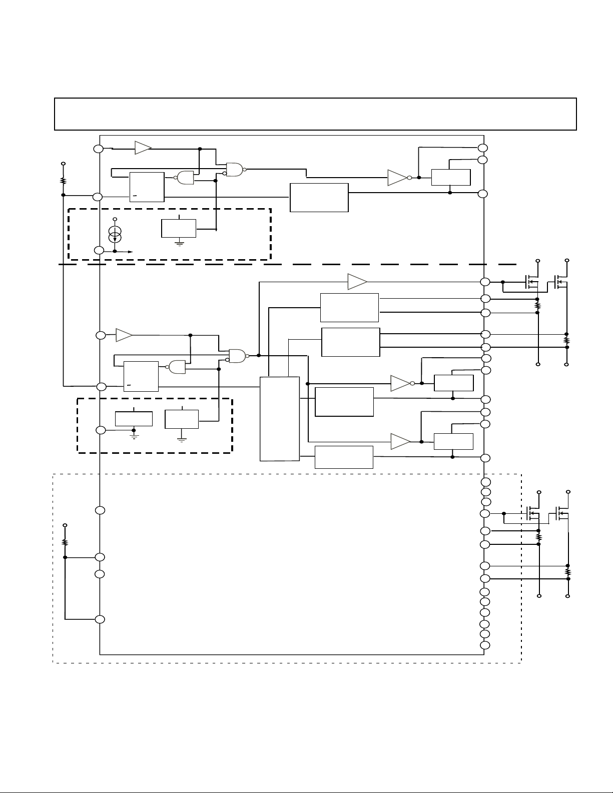
FUNCTIONAL BLOCK DIAGRAM
REV. PrN 1/02
Information furnished by Analog Devices is believed to be accurate and
reliable. However, no responsibility is assumed by Analog Devices for its
use, nor for any infringements of patents or other rights of third parties
which may result from its use. No license is granted by implication or
otherwise under any patent or patent rights of Analog Devices.
TM
Hot Plug is a trademark of Core International, Inc.
One Technology Way, P.O. Box 9106, Norwood, MA 02062-9106, U.S.A.
Tel: 781/329-4700 www.analog.com
Fax: 781/326-8703 © Analog Devices, Inc., 2002
Page 2

ADM1014–SPECIFICATIONS
FEATURES
Controls Two PCI Slots
Controls all Four PCI Supplies, +3.3V, +5V, +12V,
-12V, plus 3.3V auxiliary supply
Internal MOSFET Switches for +3.3V AUX, +12V
and –12V outputs
Adjustable Overcurrent Protection for all Outputs
Undervoltage Protection on +3.3V, +5V, +12V and
+3.3V AUX Supplies
Open-Drain Fault Output with Adjustable Delay
Logic Control of Outputs
Adjustable Soft-start
APPLICATIONS
Compact PCI
PCI Hot-Plug
GENERAL DESCRIPTION
TM
The ADM1014 is a dual PCI voltage bus controller that allows
hot-plugging of adapter cards into and out of an active or passive backplane. The device requires only four external power
MOSFETs and a few discrete components for a complete
power-control solution for two PCI slots.
The ADM1014 operates from a +12V and +3.3V AUX supply
and controls five independent supplies (+3.3V, +3.3VAUX,
+5V, +12V and –12V) on two separate channels (A and B).
The power switches for the +3.3VAUX, +12V and –12V
supplies are integrated onto the chip, and internal current
limiting is provided. For the +3.3V and +5V supplies, the
device drives external, N-channel, power MOSFETs, and
provides overcurrent protection by sensing the voltage drop
across external current-sense resistors.
The current limits for all 10 supplies are set by a single resistor
to GND, connected to the OCSET pin.
Undervoltage sensing is provided on the +3.3V, +5V, +12V
and +3.3VAux supplies. Overcurrent sensing is provided on all
supplies. In the event of an overcurrent or undervoltage fault on
any of the outputs of either channel, all outputs on that channel
will be turned off.
Turn-on slew rate may be controlled using eight external
capacitors, connected to the gate drives of all of the supplies.
Logic control of the four main outputs is provided by the
PWRONA and PWRONB pins. When these pins are high, the
outputs are turned on, when low, the outputs are turned off.
The +3.3VAUX supplies have their own control inputs,
PAUXA and PAUXB.
(Specifications are for each channel, 3.3VAUX=AUXINA=3.3V, VCC = 12VIN = +12V, -12VIN = -12V, Nominal 3.3V and 5V supplies to external
MOSFETs, TA = 0oC to +70oC, unless otherwise noted.)
Parameter Min Typ Max Units Test Conditions/Comments
5V/ 3.3V SUPPLY CONTROL
5V Overcurrent Threshold - 8 - A See Typical Application Diagram
5V Overcurrent Threshold Voltage 33 42 50 mV V
5V Overcurrent Threshold Voltage 70 80 90 mV V
OCSET
OCSET
= 0.6V
= 1.2V
5V Undervoltage Trip Threshold 4.42 4.65 4.7 V
5V Undervoltage Fault Response Time - 110 160 ns
5V Turn-On Time - 9.75 - ms C
(PWRON High to 5VOUT = 4.75V) R
= 0.033µF, C
3V5VG
= 1⍀
L
5VOUT
= 2000µF,
3V Overcurrent Threshold - 10 - A See Typical Application Diagram
3V Overcurrent Threshold Voltage 41 52 62 mV OCSET = 0.6V
3V Overcurrent Threshold Voltage 89 98 108 mV OCSET = 1.2V
3V Undervoltage Trip Threshold 2.74 2.86 2.9 V
3V Undervoltage Fault Response Time - 110 160 ns
3V5VG Undervoltage Enable Threshold - 9.6 - V
Voltage
3V Turn-On Time - 9.75 - ms C
(PWRON High to 3VOUT = 3.00V) R
= 0.033µF, C
3V5VG
= 0.43⍀
L
3VOUT
= 2000µF,
3V5VG Vout High 11.5 11.8 - V PWRON = High, FLTN = High
Gate Output Charge Current 19 25.0 29 µA PWRON = High, V
Gate Turn-On Time - 280 - µ s C
= 0.033µF,3V5VG Rising 10% to 90%
3V5VG
3V5VG
= 4V
(PWRON High to 3V5VG = 11V)
Gate Turn-Off Time - 2 - µs C
= 0.033µF, 3V5VG Falling 90% to 10%
3V5VG
+12V SUPPLY CONTROL
On Resistance of Internal PMOS - 0.3 0.35 ⍀ PWRON = High, ID = 0.5A, TA= TJ= 25oC
On Resistance of Internal PMOS - 0.35 0.5 ⍀ PWRON = High, I
Overcurrent Threshold 0.6 0.75 0.9 A V
Overcurrent Threshold 1.25 1.50 1.8 A V
OCSET
OCSET
= 0.6V
= 1.2V
= 0.5A, TA= TJ= 70oC
D
12V Undervoltage Trip Threshold 10.25 10.6 10.8 V
Undervoltage Fault Response Time - 110 - ns
–2–
REV. PrN 1/02
Page 3

ADM1014–SPECIFICATIONS (Continued)
(Specifications are for each channel, 3.3VAUX=AUXINA=3.3V, VCC = 12VIN = +12V, -12VIN = -12V, Nominal 3.3V and 5V supplies to external
MOSFETs, TA = 0oC to +70oC, unless otherwise noted.)
Parameter Min Typ Max Units Test Conditions/Comments
Gate Charge Current 19 25.0 29 µA PWRON = High, V 12VG = 10V
Turn-On Time - 16 - ms C
(PWRON High to 12VG = 1V)
Turn-Off Time - 4.5 - µs C
-12V SUPPLY CONTROL
On Resistance of Internal NMOS - 0.7 1 ⍀ PWRON = High, ID = 0.1A, TA=TJ=25oC
On Resistance of Internal NMOS - 1 1 .3 ⍀ PWRON = High, I
Overcurrent Threshold 0.13 0.18 0.25 A V
Overcurrent Threshold 0.23 0.38 0.52 A V
Gate Output Charge Current 19 25 29 µA PWRON = High, V
Turn-On Time - 16 - ms C
(PWRON High to M12VO = -10.8V)
Turn-Off Time - 3 - µs C
M12VIN Input Bias Current - 2.5 5 mA PWRON = High
+3.3VAUX SUPPLY CONTROL
On Resistance of Internal PMOS - 0.25 TBD ⍀ PAUXON = High, I
On Resistance of Internal PMOS - 0.25 TBD ⍀ PAUXON = High, I
Overcurrent Threshold - 0.5 TBD A V
Overcurrent Threshold - 1.0 TBD A V
3.3VAUX Undervoltage Trip Threshold - 2.9 TBD V
Undervoltage Fault Response Time - 110 - ns
Gate Charge Current 19 25.0 29 µA PAUXON = High, V
Turn-On Time
(PAUXON High to AUXG = 1V) - 16 - ms C
Turn-Off Time - 3 - µs C
3.3VAUX Power On Reset Threshold - 2.5 - V AUXIN Voltage Rising
CONTROL PINS
12VIN Supply Current - 5.3 8 mA
AUXIN Supply Current - 3 TBD mA
OCSET Current 93 100 107 µA
Overcurrent to Fault Response Time - 500 960 ns
PWRONA/B, PAUXA/B Threshold Voltage 1.0 1.6 2.1 V
12V Power On Enable Threshold 9.4 10 10.2 V 12VINA Voltage Rising
12V Power On Reset Threshold 8.9 9.1 9.3 V 12VINA Voltage Falling
FAULT O/P PINS
FLTA/B Output Low Voltage - 0.5 0.7 V I
FLTA/B Output High Voltage
AUXIN
-0.5
AUXIN
-0.1 - V I
FLTA/B, Output Latch Threshold TBD 1.6 TBD V I
FAUXA/B Output Low Voltage - 0.5 0.7 V I
FAUXA/B Output High Voltage
AUXIN
-0.5
AUXIN
-0.1 - V I
FAUXA/B Output Latch Threshold TBD 1.6 TBD V I
= 0.033µF, 12VG Falling 90% - 10%
12VG
= 0.033µF, 12VG Rising 10% - 90%
12VG
= 0.1A, TA=TJ=70oC
= 0.6V
OCSET
= 1.2V
OCSET
= 0.033µF, C
M12VG
=0.033µF,M12VG Falling 90% -10%
M12VG
= 0.6V
OCSET
= 1.2V
OCSET
= 0.033µF
AUXG
= 0.033µF, AUXG Rising 10% - 90%
AUXG
= 2mA
FLT
= 0
FLT
High to Low transition
FLT
= 2mA
FAUX
= 0
FAUX
High to Low transition
FAUX
D
= -10V
M12VG
= 50µF,RL= 120⍀
M12VO
= 0.375A, TA=TJ=25oC
D
= 0.375A, TA=TJ=70oC
D
= 3V
AUXG
NOTES
Specifications subject to change without notice.
–3–REV. PrN 1/02
Page 4
ADM1014–SPECIFICATIONS
ABSOLUTE MAXIMUM RATINGS*
(TA = +25°C unless otherwise noted)
VCC , 12VIN . . . . . . . . . . . . . . . . . . . . . . . . .-0.5V to +14.0V
12VO, 12VG, 3V5VG . . . . . . . . . . -0.5V to V 12VIN +0.5V
-12VIN . . . . . . . . . . . . . . . . . . . . . . . . . . . . -14.0V to +0.5V
-12VO, -12VG . . . . . . . . . . . . . . . . . . . V
-0.5V to +0.5V
-12VIN
3VISEN, 5VISEN . . . -0.5V to the Lesser of 12VIN or +7.0V
Voltage, Any Other Pin . . . . . . . . . . . . . . . . . .-0.5V to +7.0V
12VO Output Current . . . . . . . . . . . . . . . . . . . . . . . . . . . . 3A
-12VO Output Current . . . . . . . . . . . . . . . . . . . . . . . . . . 0.8A
Continuous Power Dissipation (T
TSSOP (derate 8.3mW/
o
= +70oC) . . . . . . 667mW
A
C above +70oC)
Operating Temperature Range
Commercial (J Version) . . . . . . . . . . . . . . . . 0°C to +70°C
Storage Temperature Range . . . . . . . . . . . –65°C to +150°C
Lead Temperature (Soldering, 10 sec) . . . . . . . . . . . +300°C
*This is a stress rating only and functional operation of the device at these or any
other conditions above those indicated in the operation sections of this specification is not implied. Exposure to absolute maximum rating conditions for
extended periods of time may affect reliability.
THERMAL CHARACTERISTICS
38-Pin TSSOP Package:
q
= 100°C/Watt, q
JA
= 10°C/Watt
JC
ORDERING GUIDE
Temperature Package Package
Model Range Description Option
ADM1014JRU 0°C to +70°C 38-Pin TSSOP RU-38
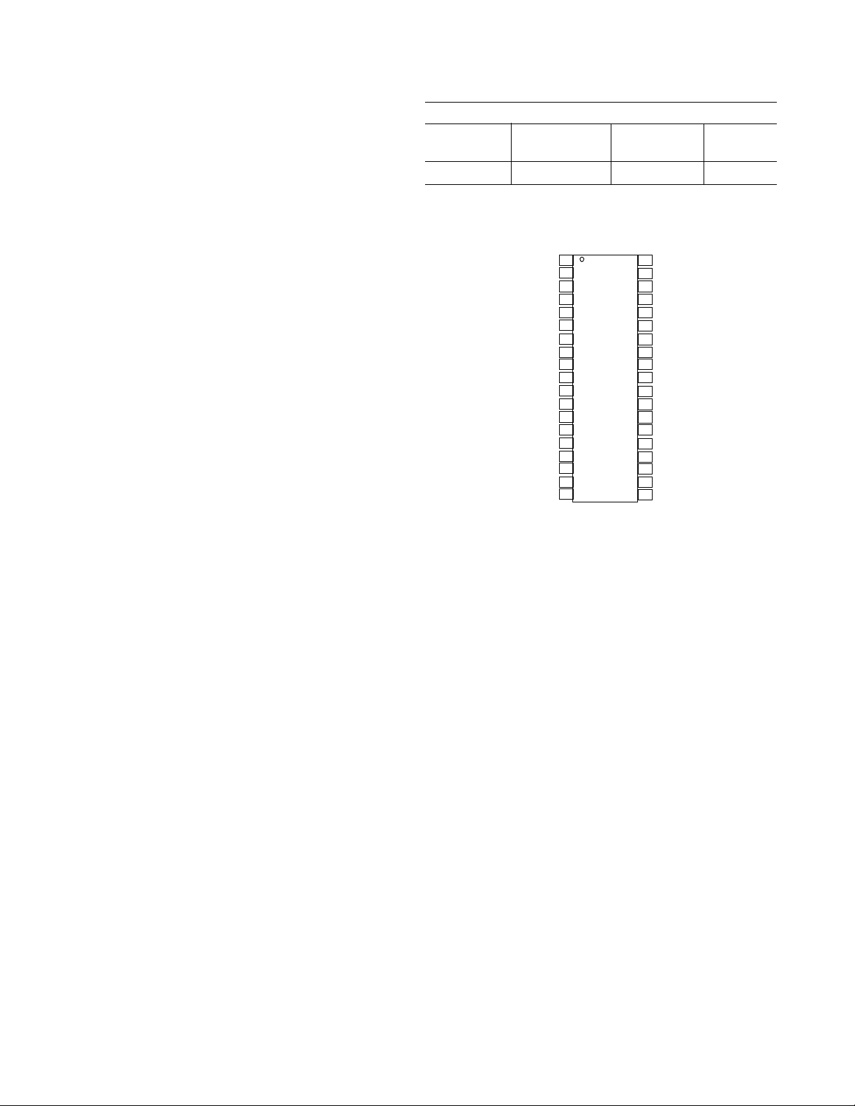
PIN CONFIGURATION
M12VOA
M12VGA
PWRO N A
FLTNA
FAUXA
OCSET
AUXGA
AUXOA
12VGA
12VOA
12VOB
12VGB
AUXOB
AUXGB
FAUXB
FLTNB
PWRO N B
M12VGB
M12VOB
1
2
3
4
5
6
7
8
9
ADM1014
10
TOP VIEW
(Not to Scale)
11
12
13
14
15
16
17
18
19
38
37
36
35
34
33
32
31
30
29
28
27
26
25
24
23
22
21
20
M12VINA
3VISENA
3VSA
5VISENA
5VSA
3V5VGA
GND
AUXINA
PAUX ONA
12VINA
12VINB
PAUX ONB
AUXINB
3V5VGB
5VSB
5VISENB
3VSB
3VISENB
M12VINB
–4–
REV. PrN 1/02
Page 5

ADM1014
PIN FUNCTION DESCRIPTION
Pin Mnemonic Function
1 M12VOA Switched -12V output for channel A. Rated for 100mA.
2 M12VGA Gate of channel A internal NMOS transistor. A capacitor connected from this pin to -12VOA (pin 1)
sets the start-up ramp for the +12V supply. During turn-on, this capacitor is charged from a 25µA
current source.
3 PWRONA Power on control for channel A. 3.3V CMOS-compatible logic input controls all four main supplies.
PWRONA high = outputs on, PWRONA low = outputs off.
4 FLTNA Active-low, 5V compatible, Open Drain fault output for channel A. A pull-up resistor connects the
pin to 3.3VAux. 4.7k⍀ is recommended for this function. An optional capacitor may be connected
from this pin to GND to provide improved immunity to power supply transients.
5 FAUXA Active-low, 3.3V compatible, Open Drain fault output for Aux channel A. The same pull-up resistor
as that on FLTNA connects the pin to 3.3VAux.
6 OCSET Overcurrent set for all 10 outputs. A resistor connected from this pin to ground sets the overcurrent
trip point of all eight supplies. All eight overcurrent trip-points can be programmed by changing the
value of this resistor. The default value of 6.04k⍀, ±1% is compatible with the maximum currents
allowed by the PCI specification.
7 AUXGA Gate of channel A +3.3VAUX internal PMOS transistor. A capacitor connected from this pin to
AUXOA (pin 8) sets the start-up ramp for the +3.3VAUX supply. During turn-on, this capacitor is
charged from a 25µA current source.
8 AUXOA Switched 3.3V auxiliary output for channel A. Rated for 0.375A.
9 12VGA Gate of channel A internal PMOS transistor. A capacitor connected from this pin to 12VOA (pin 10)
sets the start-up ramp for the +12V supply. During turn-on, this capacitor is charged from a 25µA
current source. The undervoltage circuitry is disabled when the voltage on 12VGA rises above 1.2V.
If the capacitor on pin 7 (AUXGA) or pin 33 (3V5VGA) is more than 25% larger than the capacitor on
pin 9 (12VGA) a false undervoltage condition may be detected during startup.
10 12VOA Switched 12V output for channel A. Rated for 0.5A.
11 12VOB Switched 12V output for channel B. Rated for 0.5A.
12 12VGB Gate of channel B internal PMOS transistor. A capacitor connected from this pin to 12VOB (pin 11)
sets the start-up ramp for the +12V supply. During turn-on, this capacitor is charged from a 25µA
current source. The undervoltage circuitry is disabled when the voltage on 12VGB rises above 1.2V.
If the capacitor on the pin 25 (3V5VGB) or pin 14 (AUXGB) is more than 25% larger than the
capacitor on pin 12 (12VGB) a false undervoltage condition may be detected during startup.
13 AUXOB Switched 3.3V auxiliary output for channel B. Rated for 0.375A.
14 AUXGB Gate of channel B +3.3VAUX internal PMOS transistor. A capacitor connected from this pin to
AUXOB (pin 13) sets the start-up ramp for the +3.3VAUX supply. During turn-on, this capacitor is
charged from a 25µA current source.
15 FAUXB Active-low, 3.3V compatible, Open Drain fault output for Aux channel B. The same pull-up resistor
as that on FLTNA connects the pin to 3.3VAux.
16 FLTNB Active-low, 5V compatible, Open Drain fault output for channel B. A pull-up resistor connects the
pin to 3.3VAux. 4.7k⍀ is recommended for this function. An optional capacitor may be connected
from this pin to GND to provide improved immunity to power supply transients.
17 PWRONB Power on control for channel B. 3.3V CMOS-compatible logic input controls all four main supplies.
PWRONB high = outputs on, PWRONB low = outputs off.
18 M12VGB Gate of channel B internal NMOS transistor. A capacitor connected from this pin to -12VOB (pin 19)
sets the start-up ramp for the +12V supply. During turn-on, this capacitor is charged from a 25µA
current source.
19 M12VOB Switched -12V output for channel B. Rated for 100mA.
REV. PrN 1/02
–5–
Page 6

ADM1014
PIN FUNCTION DESCRIPTION (CONTINUED)
Pin Mnemonic Function
20 M12VINB -12V supply input for channel B. Also provides power to the -12V overcurrent circuitry.
21 3VISENB 3.3V current sense for channel B. A current-sensing resistor is connected between this pin and 3VSB
(pin 22). Connect to the load side of the current sense resistor.
22 3VSB 3.3V source for channel B. The source of the 3.3V MOSFET is connected to this pin and a
current-sensing resistor is connected between this pin and pin 21.
23 5VISENB 5V current sense for channel B. A current-sensing resistor is connected between this pin and 5VSB
(pin 24). Connect to the load side of the current sense resistor.
24 5VSB 5V source for channel B. The source of the 5V MOSFET is connected to this pin and a
current-sensing resistor is connected between this pin and pin 23.
25 3V5VGB 3.3V and 5V gate output for channel B, drives the gates of the external 3.3V and 5V MOSFETs.
A capacitor connected from this pin to GND sets the start-up ramp for the 3.3V and 5V supplies.
During turn-on, this capacitor is charged from a 25µA current source. The undervoltage circuitry is
disabled when the voltage on 3V5VGB falls below 12VIN-1.2V.
26 AUXINB +3.3V auxiliary supply input for channel B.
27 PAUXONB Power on control for channel B +3.3V auxiliary output. 3.3V CMOS-compatible logic input.
PAUXONB high = outputs on, PAUXONB low = outputs off.
28 12VINB Switched +12V supply input for channel B.
29 12VINA Switched +12V supply input for channel A and for OCSET and power-on RESET circuits.
30 PAUXONA Power on control for channel A +3.3V auxiliary output. 3.3V CMOS-compatible logic input.
PAUXONA high = outputs on, PAUXONA low = outputs off.
31 AUXINA +3.3V auxiliary supply input for channel A.
32 GND Ground for all chip circuits. Connect to common of power supplies.
33 3V5VGA 3.3V and 5V gate output for channel A, drives the gates of the external 3.3V and 5V MOSFETs. A
capacitor connected from this pin to GND sets the start-up ramp for the 3.3V and 5V supplies.
During turn-on, this capacitor is charged from a 25µA current source. The undervoltage circuitry is
disabled when the voltage on 3V5VGA falls below 12VIN-1.2V.
34 5VSA 5V source for channel A. The source of the 5V MOSFET is connected to this pin and a
current-sensing resistor is connected between this pin and pin 35.
35 5VISENA 5V current sense for channel A. A current-sensing resistor is connected between this pin and 5VSA
(pin 34). Connect to the load side of the current sense resistor.
36 3VSA 3.3V source for channel A. The source of the 3.3V MOSFET is connected to this pin and a
current-sensing resistor is connected between this pin and pin 37.
37 3VISENA 3.3V current sense for channel A. A current-sensing resistor is connected between this pin and 3VSA
(pin 36). Connect to the load side of the current sense resistor.
38 M12VINA -12V supply input for channel A. Also provides power to the -12V overcurrent circuitry.
–6–
REV. PrN 1/02
Page 7

FAUX
PAUXON
ADM1014
AUXG
V
V
C
C
CURRENT
TRACKING
COMP
V
OCSET
/1.2
AND
I-V CONVERTER
C
C
AUXIN
AUXO
FLT
OCSET
GND
ZENER
REFERENCE
V
CC
100µA
12V IN
POWER-ON
RESET
V
CC
COMMON
TO BOTH
CHANNELS
VOCSET
V
CC
LOW WHEN
V
< 10V
CC
COMP
COMP
COMP
V
OCSET
V
V
OCSET
OCSET
COMP
INHIBIT
COMP
INHIBIT
COMP
INHIBIT
/14.5
/11.5
CURRENT TRACKING
/0.8
I-V CONVERTER
V
AND
10.8V
CC
4.6V
2.9V
V
CC
-12VIN
5VISEN
5VS
3V5VG
3VISEN
3VS
12VG
12VIN
12VO
-12VG
-12VIN
PWRON
CIRCUIT OF ONE CHANNEL SHOWN
REV. PrN 1/02
CURRENT
TRACKING
V
/3.3
COMP
, BOTH CHANNELS ARE IDENTICAL. RESET AND OCSET CIRCUITRY WITHIN DASHED LINE IS COMMEON TO BOTH CHANNELS
OCSET
AND
I-V CONVERTER
V
CC
Figure 1. Simplified Schematic
–7–
-12VO
3V5VG
Page 8

ADM1014
FUNCTIONAL DESCRIPTION
VOLTAGE OUTPUTS
The ADM1014 consists of two independent, identical channels, A and B, each of which controls four main power supply
voltages and an auxiliary voltage. As the channels are identical,
the following description applies to either channel, except
where otherwise stated.
An on-chip PMOS transistor connected between 12VIN and
12VO switches the +12V supply at currents up to 1.5A, whilst
an on-chip NMOS transistor connected between -12VIN and
-12VO switches the –12V supply at currents up to 0.38A. The
+3.3V and +5V supplies are switched by external, N-channel
MOSFETs, whose gate drive is provided by the 3V5VG pins.
Using suitable MOSFETs, singly or in parallel, currents of
several amps may be switched with very low voltage drops.
The four main power supplies may be switched on and off
under control of the PWRON pin.
The 3.3V auxiliary supply has an on-chip PMOS transistor,
which can switch currents at up to 1A. This supply is controlled independently of the other four supplies by the
PAUXON pin.
All five supplies are protected against overcurrent and the four
positive supplies are also protected against undervoltage.
EXTERNAL CURRENT LIMIT
The external power MOSFETs are protected and overcurrent
shutdown is provided on the +3.3V and +5V supplies by external current-sense resistors and on-chip comparators.
Current-sensing resistors are connected between the +5V output pin and the 5VISEN pin, and between the +3.3V output
pin and the 3.3VISEN pin. The sense pins are connected to
the inverting inputs of the current-limit comparator directly,
while the voltage outputs are connected to the non-inverting
inputs via a reference voltage proportional to the voltage on the
OCSET pin. This voltage is V
output and V
/11.5 in the case of the 3.3V output. These
OCSET
/14.5 in the case of the 5V
OCSET
values were chosen so that the 3.3V and 5V sense resistors
could both be 5m⍀ in PCI applications.
When the voltage drop across the current-sensing resistor exceeds the reference voltage, the output of the comparator will
go high, the fault latch will be set and all four main outputs and
the auxiliary output on the channel will be turned off. The
other main channel and auxiliary channel will remain on.
The reference voltages for the current-limit comparators are set
by connecting a resistor between the OCSET pin and GND.
An on-chip, 100µA current source generates a voltage across
this resistor. The current limit may also be adjusted by the
choice of current-sensing resistor.
I
LIMIT
I
LIMIT
(3.3V) = V
= (R
(5V) = V
= (R
/(11.5 ⫻ R
OCSET
⫻ 10-4)/(11.5 ⫻ R
SET
/(14.5 ⫻ R
OCSET
⫻ 10-4)/(14.5 ⫻ R
SET
SENSE3
SENSE5
)
SENSE3
)
SENSE5
)
)
Where:
I
= current limit in Amps
LIMIT
R
is resistor from OCSET to GND in ⍀
SET
R
is current-sense resistor in ⍀
SENSE
–8–
Note: The OCSET current source obtains its power supply
from 12VINA.
INTERNAL CURRENT LIMIT
The +3.3VAUX, +12V and –12V supplies have the power
MOSFET switches on-chip. These devices are protected and
overcurrent shutdown is provided by a completely self-contained
current sensing system. The output current through the on-chip
power MOSFET is tracked at a lower level by a second, smaller
MOSFET. The current through this MOSFET is then converted to a voltage, which is compared to a reference voltage
determined by R
. In the case of the +12V and -12V outputs,
SET
if the current-sense voltage exceeds this reference voltage, the
comparator output will go high, the fault latch will be set and
all four main outputs and the auxiliary output will be turned
off. Similarly in the case of the auxiliary output, if the currentsense voltage exceeds the reference voltage, the comparator
output will go high, the fault latch will be set, FAUXN/FLTN
will go low, and the auxiliary output and the four main outputs
will turn off.
The typical internal limiting currents may be calculated as follows:
I
(+3.3VAUX) = V
LIMIT
I
(+12V) = 1.25 ⫻ V
LIMIT
I
(-12V) = V
LIMIT
= (10-4 ⫻ R
= 1.25 ⫻ 10-4 ⫻ R
= (10-4 ⫻ R
OCSET
OCSET
/1.2
OCSET
/3.3
SET
SET
)/1.2
SET
)/3.3
Where:
I
= current limit in Amps
LIMIT
R
is resistor from OCSET to GND in ⍀
SET
Due to tolerances in the current tracking FETs, the variations
in the internal current limit are quite wide, typically ±20% of
the calculated value for the +12V supply and +35/-20% of the
calculated value for the –12V supply.
CHOICE OF R
Using the above equations, R
AND R
SET
SENSE
is chosen to set the required
SET
current limits for the +3.3VAUX, +12V and -12V supplies. Once
R
has been chosen, R
SET
SENSE3
and R
can be chosen to set the
SENSE5
current limits for the 3.3V and 5V outputs.
For PCI applications R
should be 6.04k⍀ and the current
SET
sense resistors should both be 5m⍀±1%. This will set the current limits to the maximum values for the PCI specification.
For other applications, the following limits should be noted.
1. The minimum value of R
is limited by the minimum
SET
voltage the current–limit comparators can reliably sense,
which is determined by noise, comparator offset voltage and
the overdrive required to switch the comparator. The reference voltage set by R
should not be less than 33mV for
SET
the 5V output, which has the smallest reference voltage.
The minimum recommended value for R
is 6k⍀, which
SET
gives a reference voltage of 35mV for the 5V output and
45mV for the 3.3V output.
2. The maximum value of R
is limited by the junction tem-
SET
perature. This is determined by the power dissipated in the onchip MOSFETs, (which is dependent upon the current passed
REV. PrN 1/02
Page 9

ADM1014
by the devices and their on-resistance), the thermal resistance
of the package (100
o
C/W), and the ambient temperature.
The maximum on-resistance of the +3.3VAUX MOSFET is
0.65⍀, that of the +12V MOSFET is 0.35⍀ and that of the –
12V MOSFET is 0.9⍀, so the power dissipation will be:
P
= (0.65 ⫻ (I
D
+3.3VAUX
)2 + 0.35 ⫻ (I
)2 + 0.9 ⫻ (I
+12V
-12V
)2)
Where:
P
is power dissipation in Watts
D
I is current in Amps
Under normal operating conditions the maximum recom-
mended value for R
UNDERVOLTAGE SENSING
is 15k⍀.
SET
Undervoltage sensing of the +3.3V, +5V, +12V and
+3.3VAUX supplies is carried out by four voltage comparators.
The supply voltages being monitoring are applied to the
inverting inputs of these comparators, whilst reference voltages
of 2.9V, 4.6V, 10.8V and 2.9V (derived from an on-chip zener
reference) are applied to their non-inverting inputs. Should any
of the output voltages fall below the corresponding reference
voltage, the output of the comparator will go high, the fault
latch will be set, turning off all the supplies (main and auxiliary)
on that channel.
FLTN AND FAUXN OUTPUTS
The FLTN and FAUXN outputs are active-low, 3.3V compatible,
Open- Drain fault outputs. These outputs are shorted together and
then connected to the 3.3VAux supply using a 4.7k⍀ pull-up
resistors. Should an overcurrent or undervoltage event occur on one
of the supplies, main or auxiliary, then the fault latch will be set,
FLTA and FAUXA or FLTB and FAUXB will go low and all
outputs on the faulting channel will be turned off.
PROGRAMMABLE FAULT LATCH DELAY
The delay between an overcurrent or undervoltage fault occurring and the outputs shutting down may be set by connecting a
capacitor between a FLTN or FAUXN output and GND. This
delays the start of the FLTN/FAUXN output 1 to 0 transition
and slows down the fall time of the FLTN/FAUXN output,
thus delaying shutdown of the outputs. If the fault latch threshold (~1.6V) is reached on FLTN/FAUXN then the fault latch
will be set and the four supply outputs and the auxiliary output
will be shut down. If the fault disappears before the latching
threshold is reached, the fault latch will not be set and the
FLTN/FAUXN output will return to a high state.
This adjustable delay allows the ADM1014 to ignore overcurrent
and undervoltage transients that might otherwise cause an unwanted shutdown. It should be noted that if a fault is asserted
on FLTN and FAUXN at the same time, then the delay is
halved, as shown in fig. 2 and Table 1.
Figure 2. FLTN and 3V5VG Delay
TABLE 1. FLT AND 3V5VG DELAY VS. C
C
FLT
t
A
FLT
t
2A
OPEN 0.1µs 0.05µs
0.001µF 0.44µs 0.22µs
0.01µF 2.9µs 1.5µs
0.1µF 28µs 14µs
POWER CONTROL INPUTS
The PWRONA and PWRONB inputs are 3.3V CMOS-compatible logic inputs, which may be used to switch all four main
outputs on and off, and is also used to reset the fault latch and
turn the outputs back on after an overcurrent or undervoltage
shutdown.
When PWRON is high, the four main supplies are turned on.
With PWRON held low, the supplies are turned off. After an
overcurrent or undervoltage shutdown, PWRON should be
toggled low then high again to reset the fault latch and turn on
the outputs.
PAUXONA and PAUXONB are also 3.3V CMOS-compatible
logic inputs which perform a similar function for the +3.3V
auxiliary supplies.
POWER-ON SEQUENCE AND SOFT START
When the device is powered on with PWRON held high, the
outputs are inhibited by the power-on reset circuit and will not
become active until V
exceeds 10V. During this time the
CC
undervoltage comparators are inhibited and the fault latch is
held in a reset condition.
Note: the power-on reset circuit monitors 12VINA.
After the power-on delay, all five outputs are turned on simultaneously. The undervoltage comparators are enabled when the
voltage on the gate of the internal PMOS transistor, 12VG, has
fallen below about 400mV.
The rise time of the outputs may be controlled by connecting
capacitors between the gate and output pins of the +3.3VAUX,
+12V and -12V outputs, and from the 3V5VG pin to GND.
During output turn-on, these capacitors are charged from a
nominal 25µA current source. Limiting the output rise times
also limits the charging currents drawn by any supply
decoupling capacitors in the circuits being driven. With fast
turn-on these currents might be excessive and cause
overcurrent faults at power-on.
Care must be taken when choosing these capacitors. If the
capacitor on AUXG or 3V5VG is more than 25% larger than
REV. PrN 1/02
–9–
Page 10

ADM1014
the capacitor on 12VG, the +3.3VAUX, 3.3V and 5V outputs
may not have exceeded their undervoltage thresholds by the
time the undervoltage comparators are enabled, and a false
undervoltage condition may be detected. For this reason it is
recommended to use the same value for all three gate capacitors.
For PCI applications the minimum recommended value is
0.033µF. Smaller values may cause overcurrent faults at powerup due to excessive charging currents drawn by decoupling
capacitors.
The maximum value of the gate capacitors is determined by the
need to discharge them quickly when turning off the outputs
under fault conditions. If the capacitors are too large the
ADM1014 may be unable to protect the power bus or the external MOSFETs. With 0.033µF capacitors, the turn-off time
will be less than 6µs.
-12V
+3.3 Vau x
C1
C2
C3
C4
C5
C6
AUXINA
AUXGA
AUXOA
M12VINA
M12GA
M12VOA
M12VINB
M12GB
M12VOB
12VINA
12VGA
12VOA
12VINB
12VGB
12VOB
AUXINB
AUXGB
AUXOB
PAUXONA
PWRONA
PWRONB
PAUXONB
FLTNA
FAUXA
FROM
SYSTEM
CONTROLLER
+12V BUS
+3.3Vaux BUS
12V
-12V BUS
APPLICATIONS INFORMATION
APPLICATION CIRCUIT
Figure 3 shows a typical circuit configuration for the ADM1014 in
a PCI application, controlling supply voltages of +3.3V at up to
7.6A, +5V at up to 5A, +12V at up to 0.5A and –12V at up to
0.1A. In this circuit, two external MOSFETs are connected in
parallel for the 3.3V and 5V outputs to minimise on-resistance.
5V
Q1
Q2
Q3
Q4
R1
R2
R3
R4
3.3V
5V BUS
3.3V BUS
SLOT 1
ADM1014
FLTNB
FAUXB
5VISENA
5VISENB
3VISENA
3VISENB
OCSET
5VSA
3V5VGA
3V5VGB
5VSB
3VSA
3VSB
C7 C8
GND
12V
-12V
+3.3 Vau x
R11
R12
C10
C9
TO SYSTEM CONTROLLER
C11 C12
SLOT 2
Figure 3. Typical Application Circuit
–10–
R5
3.3V
5V
REV. PrN 1/02
Page 11

250mA
50mA
375mA
2A
3A
+12V
-12V
3.3Vaux
5.0V
3.3V
ADM1014
RL1
C1
RL2
C2
RL3
C3
RL4
C4
RL5
C5
GND
Figure 4. Load Board for Typical Application Circuit
Mai n Boa rd Component s
Item Qty Ref Des Description
1 1 U1 ADM1014
2 1 SKT1 38 Pin Tssop Socket
3 4 Q1-4 IRF7413 Power Mosfet
4 4 D1-4 Green SMD LED
5 4 R1-4 5m
6 2 R5-6 470
7 2 R7-8 1K5
8 2 R9-10 6K04
⍀
Metal Strip Resistor
⍀
0805 chip resistor
⍀
0805 chip resistor
⍀
0805 chip resistor
9 8 C1-8 CAP,0.033UF
10 4 C9-12 CAP,0.47UF
11 3 C13-15 Electrolytic capacitor space
12 1 S1 SPDT Slide Switch
13 8 T1-8 Testpoint
14 2 P1-2 20 Pin Edge Conn Skt
15 4 J1 J4-J6 4mm 10A PCB Sockets-Red
16 1 J2 4mm 10A PCB Sockets-Green
17 1 J3 4mm 10A PCB Sockets-Black
18 4 P4-7 SMB
19 1 PCB EVAL-ADM1014 Main Board
⍀
20 4 R11-12 4K7
0805 chip resistor
21 2 Load Board Fully Assembled Load Board
Load Board Components
Item Qty Ref Des Description
1 1 PCB EVAL-ADM1014Load Board
2 3 CL1-CL3 100uF 16V Electrolytic Caps
3 2 CL4-CL5 2200uF 16V Electrolytic Caps
⍀
4 1 RL1 47
5 1 RL2 240
6 1 RL3 10
7 1 RL4 2.2
8 1 RL5 1
6W (W22 Series) Res
⍀
2.5W (W21 Series) Res
⍀
6W (W22 Series) Res
⍀
12W (W24 Series) Res
⍀
12W (W24 Series) Res
REV. PrN 1/02
–11–
Page 12

ADM1014
LAYOUT CONSIDERATIONS
Any circuits supplied by the ADM1014 are outside the control
loops of the main system power supplies, which means that any
series resistance between the four supply inputs and the outputs will cause a degradation of the supply load regulation. This
includes connector contact resistance, PCB trace resistance, onresistance of MOSFETs (both external and on-chip) and
current sense resistors.
Care must therefore be taken to ensure that:
a)PCB traces are as heavy as possible.
b)External MOSFETs have low-on resistance.
c)Current sense resistors are as small as possible.
The current sense resistors have very small values (5m⍀ in the
preceding example) to minimise the voltage drop across them.
Because of this, PCB trace resistance can be a significant percentage of the sense resistance. It is therefore essential to ensure that the ADM1014 senses the voltage drop directly across
the sense resistors and not across any current-carrying trace
resistance in series with them. Connections from the ADM1014 to
the sense resistors must go directly to the ends of the resistors.
Figure 4 shows examples of good and bad practice
CURRENT
SENSE
RESISTORS
353437
36
222124
23
ADM1014
CORRECT
CURRENT
SENSE
RESISTORS
37
35
36
34
VSEN SE
34
21
VSENSE
ADDITIONAL
VOLTAGE DROP
VSENSE
ADDITIONAL
VOLTAGE DROP
ADDITIONAL
VOLTAGE DROP
22
21
ADM1014
24
23
VSEN SE
ADDITIONAL
VOLTAGE DROP
INCORRECT
Figure 4. Good and Bad Practice For Sense Resistor
Connection
OUTLINE DIMENSIONS
Dimensions shown in inches and (mm).
38-Pin TSSOP (RU-38)
0.386 (9.80)
0.378 (9.60)
38
20
0.177 (4.50)
0.169 (4.30)
191
0.256 (6.50)
0.246 (6.25)
PIN 1
0.006 (0.15)
0.002 (0.05)
SEATING
PLANE
0.0200 (0.50)
BSC
0.0106 (0.27)
0.0067 (0.17)
0.0433 (1.10)
MAX
0.0079 (0.20)
0.0035 (0.090)
88
08
0.028 (0.70)
0.020 (0.50)
–12–
REV. PrN 1/02
 Loading...