

Page 1

2.5 GHz to 2.7 GHz
V
V
FEATURES
Gain: 29 dB
Operation from 2.5 GHz to 2.7 GHz
EVM ≤ 3% with 16 QAM OFDMA
@ P
= 25 dBm (3.3 V, 2.6 GHz)
OUT
@ P
= 27 dBm (5 V, 2.6 GHz)
OUT
Input matched to 50 Ω
Power supply: 3.2 V to 5 V
Quiescent current: 135 mA
Power-added efficiency (PAE)
21% @ P
Multiple operating modes to reduce battery drain
Standby mode: 9 mA
Sleep mode: <1 μA
APPLICATIONS
WiMAX mobile terminals and CPEs
= 25 dBm (3.3 V, 2.6 GHz)
OUT
WiMAX Power Amplifier
ADL5571
GENERAL DESCRIPTION
The ADL5571 is a high linearity 2.5 GHz to 2.7 GHz power
amplifier designed for WiMAX mobile terminals and CPEs
using TDD operation at a duty cycle of 50% or lower. With a
gain of 29 dB and an output compression point of 31 dBm, it
can operate at an output power level up to 27 dBm while
maintaining an EVM of ≤3% with a supply voltage of 5 V. PAE
is 21% at P
The ADL5571 RF input is matched to provide an input return
loss of better than 10 dB. The open-collector output is externally
matched with a microstrip line and an external shunt capacitor.
The ADL5571 operates over a supply voltage range from 3.2 V
to 5 V with a current of 450 mA burst rms when delivering
25 dBm (3.3 V supply). A standby mode is available that reduces
the quiescent current to 9 mA, which is useful when a TDD
terminal is receiving data.
The ADL5571 is fabricated in a GaAs HBT process and is packaged
in a 4 mm × 4 mm, 16-lead, Pb-free, RoHS-compliant LFCSP
that uses an exposed paddle for excellent thermal impedance. It
operates from −40°C to +85°C.
= 25 dBm with a 3.3 V supply voltage.
OUT
FUNCTIONAL BLOCK DIAGRAM
CC1
ADL5571
RFIN
STBY
VREG
FIRST
IM1 IM2 IM3
STAGE
SECOND
STAGE
BIAS_2BIAS_1 BIAS_3
Figure 1.
CC2
THIRD
STAGE
RFOUT
CFLT
OM
06956-001
Rev. 0
Information furnished by Analog Devices is believed to be accurate and reliable. However, no
responsibility is assumed by Anal og Devices for its use, nor for any infringements of patents or ot her
rights of third parties that may result from its use. Specifications subject to change without notice. No
license is granted by implication or otherwise under any patent or patent rights of Analog Devices.
Trademarks and registered trademarks are the property of their respective owners.
One Technology Way, P.O. Box 9106, Norwood, MA 02062-9106, U.S.A.
Tel: 781.329.4700 www.analog.com
Fax: 781.461.3113 ©2008 Analog Devices, Inc. All rights reserved.
Page 2

ADL5571
TABLE OF CONTENTS
Features .............................................................................................. 1
Applications....................................................................................... 1
General Description......................................................................... 1
Functional Block Diagram .............................................................. 1
Revision History ............................................................................... 2
Specifications..................................................................................... 3
V
= 3.3 V .................................................................................... 3
CC
V
= 5 V ....................................................................................... 4
CC
Absolute Maximum Ratings............................................................ 5
ESD Caution.................................................................................. 5
Pin Configuration and Function Descriptions............................. 6
Typical Performance Characteristics ............................................. 7
REVISION HISTORY
1/08—Revision 0: Initial Version
V
= 3.3 V .....................................................................................7
CC
V
= 5 V ........................................................................................9
CC
Applications Information.............................................................. 11
Basic Connections...................................................................... 11
64 QAM OFDMA Performance............................................... 12
Power-Added Efficiency............................................................ 12
Evaluation Board ............................................................................ 13
Measurement Setup........................................................................ 14
Outline Dimensions ....................................................................... 15
Ordering Guide .......................................................................... 15
Rev. 0 | Page 2 of 16
Page 3
ADL5571
SPECIFICATIONS
VCC = 3.3 V
T = 25°C, 1024 FFT, 16 QAM OFDMA modulated carrier, 10 MHz channel BW, f = 2.6 GHz, ZL = 50 Ω, STBY = 0 V, VREG = 2.85 V, 31%
duty cycle, ACPR integration BW = 100 kHz (5.05 MHz offset) or 1 MHz (6.5 MHz, 11 MHz, 15 MHz, and 20.5 MHz offset), unless
otherwise noted.
Table 1.
Parameter Conditions Min Typ Max Unit
FREQUENCY RANGE See Tab le 5 for tuning details 2.5 2.7 GHz
LINEAR OUTPUT POWER
GAIN 29 dB
vs. Frequency ±5 MHz ±0.2 dB
vs. Temperature −40°C ≤ TA ≤ +85°C ±2 dB
vs. Supply 3.2 V to 4.2 V ±0.3 dB
OUTPUT P1dB Unmodulated pulse input 31 dBm
EVM P
INPUT RETURN LOSS 20 dB
ACPR P
HARMONIC DISTORTION 45 dBc
SUPPLY CURRENT P
QUIESCENT CURRENT No signal at RF input 135 mA
PAE P
STANDBY MODE CURRENT VREG = 2.85 V, STBY = 2.5 V 9 mA
SLEEP MODE CURRENT VREG = 0 V <1 μA
TURN-ON/-OFF TIME 1 μs
VSWR SURVIVABILITY 10:1
EVM ≤ 3%
= 25 dBm 3 % rms
OUT
= 25 dBm
OUT
±5.05 MHz carrier offset
±6.5 MHz carrier offset
±11 MHz carrier offset
±15 MHz carrier offset
±20.5 MHz carrier offset
= 25 dBm 450 mA
OUT
= 25 dBm 21 %
OUT
25 dBm
−27 dBm
−19 dBm
−24 dBm
−30 dBm
−39 dBm
Rev. 0 | Page 3 of 16
Page 4
ADL5571
VCC = 5 V
T = 25°C, 1024 FFT, 16 QAM OFDMA modulated carrier, 10 MHz channel BW, f = 2.6 GHz, ZL = 50 Ω, STBY = 0 V, VREG = 2.85 V, 31%
duty cycle, ACPR integration BW = 100 kHz (5.05 MHz offset) or 1 MHz (6.5 MHz, 11 MHz, 15 MHz, and 20.5 MHz offset), unless
otherwise noted.
Table 2.
Parameter Conditions Min Typ Max Unit
FREQUENCY RANGE See Tab le 5 for tuning details 2.5 2.7 GHz
LINEAR OUTPUT POWER EVM ≤ 3% 27 dBm
GAIN 27.5 dB
vs. Frequency ±5 MHz ±0.1 dB
vs. Temperature −40°C ≤ TA ≤ +85°C ±2.5 dB
vs. Supply 4.5 V to 5.5 V ±0.2 dB
OUTPUT P1dB Unmodulated input 32 dBm
EVM P
INPUT RETURN LOSS P
ACPR P
HARMONIC DISTORTION P
SUPPLY CURRENT P
QUIESCENT CURRENT No signal at RF input 135 mA
PAE P
STANDBY MODE CURRENT VREG = 2.85 V, STBY = 2.5 V 9 mA
SLEEP MODE CURRENT VREG = 0 V <1 μA
TURN-ON/-OFF TIME 1 μs
VSWR SURVIVABILITY 10:1
= 27 dBm 3 % rms
OUT
= 27 dBm 16 dB
OUT
= 26.5 dBm
OUT
±5.05 MHz carrier offset
±6.5 MHz carrier offset
±11 MHz carrier offset
±15 MHz carrier offset
±20.5 MHz carrier offset
= 27 dBm 47 dBc
OUT
= 27 dBm 620 mA
OUT
= 27 dBm 16 %
OUT
−28 dBm
−21 dBm
−26 dBm
−29 dBm
−35 dBm
Rev. 0 | Page 4 of 16
Page 5
ADL5571
ABSOLUTE MAXIMUM RATINGS
Table 3.
Parameter Rating
Supply Voltage
V
CC
VREG 3 V
STBY 3 V
RFOUT (Modulated—Normal Power Mode)129 dBm
Output Load VSWR 10:1
Operating Temperature Range −40°C to +85°C
Storage Temperature Range −65°C to +150°C
Maximum Solder Reflow Temperature 260°C (30 sec)
1
OFDMA carrier, 16 QAM, 10 MHz channel BW, 1024 FFT.
5.0 V
Stresses above those listed under Absolute Maximum Ratings
may cause permanent damage to the device. This is a stress
rating only; functional operation of the device at these or any
other conditions above those indicated in the operational
section of this specification is not implied. Exposure to absolute
maximum rating conditions for extended periods may affect
device reliability.
ESD CAUTION
Rev. 0 | Page 5 of 16
Page 6

ADL5571
V
PIN CONFIGURATION AND FUNCTION DESCRIPTIONS
2
GND
STBY
NC
VCC
2
1
4
3
PIN 1
5VCC1
INDICATOR
6RFIN
ADL5571
7GND
TOP VIEW
8
REG
NC = NO CONNECT
(Not to S cale)
9
CFLT1
10
CFLT2
16 NC
15 RFOUT
14 RFOUT
13 NC
11
12
NC
NC
06956-002
Figure 2. Pin Configuration
Table 4. Pin Function Descriptions
Pin No. Mnemonic Description
1, 11, 12, 13, 16 NC No Connect. Do not connect these pins.
2 VCC2 This power supply pin should be connected to the supply via a choke circuit (see Figure 19).
3, 7 GND Connected to Ground.
4 STBY
When STBY is low (0 V), the device operates in transmit mode. When the radio is receiving data, STBY
can be taken high (2.5 V), reducing the supply current to 9 mA.
5 VCC1 Connect to Power Supply.
6 RFIN RF Input.
8 VREG
When VREG is low, the device goes into sleep mode, reducing the supply current to less than 1 μA.
When VREG is high (2.85 V), the device operates in its normal transmit mode. When high, VREG draws
a bias current of approximately 9 mA.
9, 10 CFLT1, CFLT2 Ground-Referenced Capacitors. These should be connected to reduce bias line noise.
14, 15 RFOUT
Unmatched RF Outputs. These parallel outputs are matched to 50 Ω using a microstrip line and shunt
capacitor. The power supply voltage should be connected to these pins through a choke inductor.
Exposed
Paddle
The exposed paddle should be soldered down to a low impedance ground plane (use multiple vias,
at least 9, to stitch together the ground planes) for optimum electrical and thermal performance.
Table 5. Operating Modes
1
Mnemonic Normal Operation Standby Mode Sleep Mode
VREG High High Low
STBY Low High X
1
X = don’t care.
Rev. 0 | Page 6 of 16
Page 7
ADL5571
TYPICAL PERFORMANCE CHARACTERISTICS
VCC = 3.3 V
T = 25°C, 1024 FFT, 16 QAM OFDMA modulated carrier, 10 MHz channel BW, ZL = 50 Ω, STBY = 0 V, VREG = 2.85 V, 31% duty cycle,
ACPR integration BW = 100 kHz (5.05 MHz offset) or 1 MHz (6.5 MHz, 11 MHz, 15 MHz, and 20.5 MHz offset), unless otherwise noted.
0.8
0.7
0.6
0.5
0.4
0.3
CURRENT (A)
0.2
0.1
2.6GHz
2.5GHz
2.7GHz
12
10
8
6
EVM (%)
4
2
2.5GHz
2.6GHz
2.7GHz
0
10 12 14 16 18 20 22 24 26 28 30
P
(dBm)
OUT
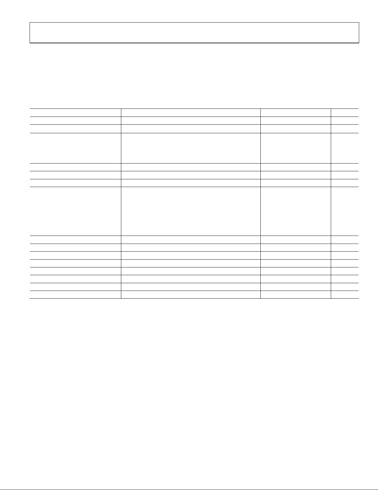
Figure 3. Burst RMS Current vs. P
at 2.5 GHz, 2.6 GHz, and 2.7 GHz
OUT
12
10
8
6
EVM (%)
4
2
0
10 12 14 16 18 20 22 24 26 28 30
P
(dBm)
OUT
Figure 4. EVM vs. P
at 2.6 GHz, Temperatures −40°C, +25°C, and +85°C
OUT
+85°C
+25°C
–40°C
0
10 12 14 16 18 20 22 24 26 28 30
P
06956-007
Figure 5. EVM vs. P
OUT
(dBm)
OUT
at 2.5 GHz, 2.6 GHz, and 2.7 GHz
06956-009
34
32
30
28
GAIN (dB)
26
24
22
2500 2520 2540 2560 2580 2600 2620 2640 2660 2680 2700
06956-008
Figure 6. Gain vs. Frequency at P
–40°C
+25°C
+85°C
FREQUENCY (MHz )
= 25 dBm,
OUT
06956-010
Temperatures −40°C, +25°C, and +85°C
Rev. 0 | Page 7 of 16
Page 8

ADL5571
–
–
–
34
32
30
28
GAIN (dB)
26
24
22
10 12 14 16 18 20 22 24 26 28 30
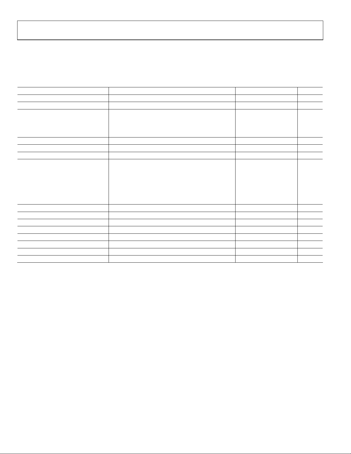
Figure 7. Gain vs. P
10
–15
–20
–25
–30
–35
–40
ACPR (dBm)
–45
–50
–55
–60
10 12 14 16 18 20 22 24 26 28 30
–40°C
+25°C
+85°C
P
(dBm)
OUT
at 2.6 GHz, Temperatures −40°C, +25°C, and +85°C
OUT
6.5MHz
11MHz
5.05MHz
15MHz
20.5MHz
P
(dBm)
OUT
Figure 8. ACPR Measurement at 2.5 GHz
06956-011
06956-012
10
–15
–20
–25
–30
–35
–40
ACPR (dBm)
–45
–50
–55
–60
10 12 14 16 18 20 22 24 26 28 30
6.5MHz
11MHz
P
5.05MHz
15MHz
20.5MHz
(dBm)
OUT
Figure 9. ACPR Measurement at 2.6 GHz
10
–15
–20
–25
–30
–35
–40
ACPR (dBm)
–45
–50
–55
–60
10 12 14 16 18 20 22 24 26 28 30
6.5MHz
11MHz
5.05MHz
15MHz
20.5MHz
P
(dBm)
OUT
Figure 10. ACPR Measurement at 2.7 GHz
06956-013
06956-014
Rev. 0 | Page 8 of 16
Page 9

ADL5571
VCC = 5 V
T = 25°C, 1024 FFT, 16 QAM OFDMA modulated carrier, 10 MHz channel BW, ZL = 50 Ω, STBY = 0 V, VREG = 2.85 V, 31% duty cycle,
ACPR integration BW = 100 kHz (5.05 MHz offset) or 1 MHz (6.5 MHz, 11 MHz, 15 MHz, and 20.5 MHz offset), unless otherwise noted.
0.9
0.8
0.7
0.6
0.5
0.4
CURRENT (A)
0.3
0.2
0.1
0
14 16 18 20 22 24 26 28 30
P
OUT
Figure 11. Burst RMS Current vs. P
2.5GHz
(dBm)
at 2.5 GHz, 2.6 GHz, and 2.7 GHz
OUT
12
2.6GHz
2.7GHz
06956-015
12
10
8
6
EVM (%)
4
2.5GHz
2
0
14 16 18 20 22 24 26 28 30
Figure 13. EVM vs. P
2.6GHz
2.7GHz
P
(dBm)
OUT
at 2.5 GHz, 2.6 GHz, and 2.7 GHz
OUT
34
06956-017
10
8
6
EVM (%)
4
2
0
14 16 18 20 22 24 26 28 30
P
OUT
Figure 12. EVM vs. P
at 2.6 GHz, Temperatures −40°C, +25°C, and +85°C
OUT
+25°C
(dBm)
+85°C
–40°C
32
30
28
GAIN (dB)
26
24
22
2500 2520 2540 2560 2580 2600 2620 2640 2660 2680 2700
06956-016
Figure 14. Gain vs. Frequency at P
–40°C
+25°C
+85°C
FREQUENCY (MHz)
= 25 dBm,
OUT
06956-018
Temperatures −40°C, +25°C, and +85°C
Rev. 0 | Page 9 of 16
Page 10

ADL5571
–
–
–
34
32
30
28
GAIN (dB)
26
24
22
14 16 18 20 22 24 26 28 30
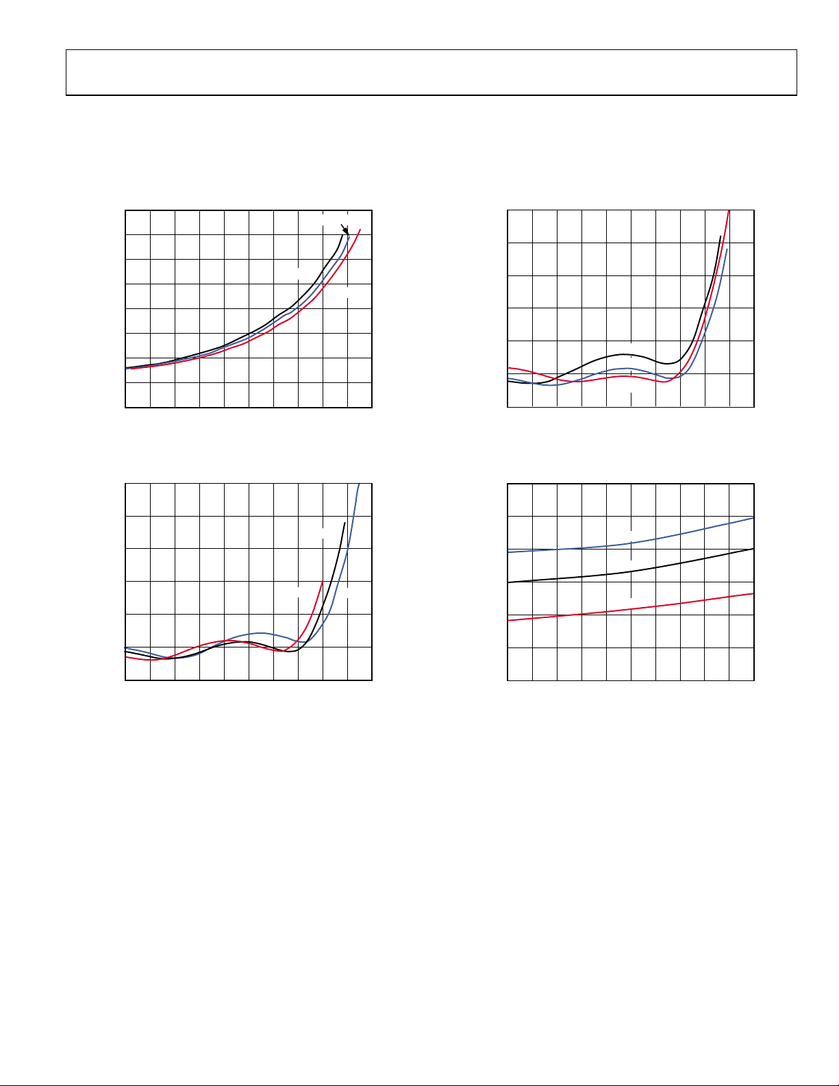
Figure 15. Gain vs. P
10
–15
–20
–25
–30
–35
–40
ACPR (dBm)
–45
–50
–55
–60
14 16 18 20 22 24 26 28 30
Figure 16. ACPR Measurement at 2.5 GHz
–40°C
+25°C
+85°C
P
(dBm)
OUT
at 2.6 GHz, Temperatures −40°C, +25°C, and +85°C
OUT
6.5MHz
11MHz
5.05MHz
15MHz
20.5MHz
P
(dBm)
OUT
06956-019
06956-020
10
–15
–20
–25
–30
–35
–40
ACPR (dBm)
–45
–50
–55
–60
14 16 18 20 22 24 26 28 30
6.5MHz
11MHz
5.05MHz
15MHz
20.5MHz
P
(dBm)
OUT
Figure 17. ACPR Measurement at 2.6 GHz
10
–15
–20
–25
–30
–35
–40
ACPR (dBm )
–45
–50
–55
–60
14 16 18 20 22 24 26 28 30
6.5MHz
11MHz
5.05MHz
15MHz
20.5MHz
P
(dBm)
OUT
Figure 18. ACPR Measurement at 2.7 GHz
06956-021
06956-022
Rev. 0 | Page 10 of 16
Page 11

ADL5571
V
V
APPLICATIONS INFORMATION
BASIC CONNECTIONS
Figure 19 shows the basic connections for the ADL5571.
POS
STBY
C6
L1
VCC1
RFIN
GND
VREG
C2
1nH
4
3
GND
STBY
ADL5571
CFLT1
9
2
CFLT
10
C10
0.01µF
2
VCC2
RFOUT
RFOUT
NC
11
VPOS1
VPOS
C7
0.01µF
RFIN
L3
2.7nH
VREG
C9
0.01µF
NC = NO CONNEC T
C8
0.01µF
5
6
7
8
2.2pF
Figure 19. Basic Connections
Power Supply
The voltage supply on the ADL5571, which ranges from
3.2 V to 4.2 V, should be connected to the VCCx pins. VCC1 is
decoupled with Capacitor C7, whereas VCC2 uses a tank circuit
to prevent RF signals from propagating on the dc lines.
RF Input Interface
The RFIN pin is the port for the RF input signal to the power
amplifier. The L3 inductor, 2.7 nH, matches the input
impedance to 50 Ω.
2.7nH
L3
Figure 20. RF Input with Matching Component
3.3pF
1
NC
NC
12
C11
1µF
VPOS1
L2
C5
11nH
16
NC
15
14
13
NC
W1
6
RFIN
06956-004
2.7pF
C4
39pF
C3
OPEN
VPOS
RFOUT
C12
1µF
06956-003
RF Output Interface
The parallel RF output ports have a shunt capacitor, C3 (2.7 pF),
and the line inductance of the microstrip line for optimized
output power and linearity. The characteristics of the ADL5571
are described for 50 Ω impedance after the output matching
capacitor (load after C3). C4 provides dc blocking on the
RF output.
POS1
RFOUT
RFOUT
15
14
11nH
L2
C4
39pF
C3
2.7pF
C5
OPEN
C12
1µF
RFOUT
06956-005
Figure 21. RF Output
Transmit/Standby Enable
During normal transmit mode, the STBY pin is biased low
(0 V). However, during receive mode, the pin can be biased
high (2.5 V) to shift the device into standby mode, which
reduces current consumption to 9 mA.
VREG Enable
During normal transmit, the VREG pin is biased to 2.85 V and
draws 9 mA of current. When the VREG pin is low (0 V), the
device suspends itself into sleep mode (irrespective of supply
biasing). In this mode, the device draws less than 1 μA of
current.
Rev. 0 | Page 11 of 16
Page 12
ADL5571
×−Ι
64 QAM OFDMA PERFORMANCE
The ADL5571 shows exceptional performance when used with
a higher order modulation scheme, such as a 64 QAM system.
Figure 22, Figure 23, and Figure 24 illuminate the EVM, gain,
and current consumption performance within the context of a
64 QAM OFDMA system.
14
13
12
11
10
9
8
7
6
EVM (%)
5
4
3
2
1
0
810121416182022242628
Figure 22. EVM vs. P
2700MHz
OUT
64 QAM OFDMA Signal
32
31
30
29
GAIN (dB)
28
27
26
2500 2520 2540 2560 2580 2600 2620 2640 2660 2680 2700
FREQUENCY (M Hz )
Figure 23. Gain vs. Frequency Performance at V
64 QAM OFDMA Signal
2500MHz
2600MHz
P
(dBm)
OUT
Performance at VCC = 3.3 V and
= 3.3 V and
CC
06956-023
06956-024
0.8
0.7
0.6
0.5
0.4
CURRENT (A)
0.3
0.2
0.1
0
0 5 10 15 20 25 30
P
OUT
Figure 24. Burst Current vs. P
(dBm)
at VCC = 3.3 V, 64 QAM,
OUT
06956-025
2350 MHz, 31% 802.16e OFDMA Signal
POWER-ADDED EFFICIENCY
The efficiency of the ADL5571 is defined on the current that it
draws during the data burst of an 802.16e OFDMA signal. In
typical test setup, the average rms current, I
However,
= Duty Cycle (in decimal) × I
I
AVG
(1 − Duty Cycle [in decimal]) × I
BURST
DEFAULT
where:
I
is the rms current during the data burst of an OFDMA
BURST
signal.
I
can be the quiescent current drawn when there is no
DEFAULT
data burst and the device remains biased, the sleep current
(<1 μA) if the device is defaulted to sleep mode, or the standby
current.
For example, in a 31% duty cycle 802.16e OFDMA signal,
the burst current is calculated by rearranging the previous
equation to get
AVG
=
I
BURST
I
0.31
DEFAULT
)0.69(
Finally, the PAE is calculated by
(%)
PAE
=
−
(mA)(V)
×
CC
IV
BURST
When RF is 2.6 GHz, 31% 16 QAM OFDMA signal,
is 3.3 V, RF Output Power is 25 dBm, and RF Input
V
CC
Power is −4 dBm, the ADL5571 consumes a burst current,
is 450 mA and PAE = 21%.
I
BURST
, is measured.
AVG
+
(mW)(mW)
PowerInputRFPowerOutputRF
100
×
Rev. 0 | Page 12 of 16
Page 13

ADL5571
EVALUATION BOARD
The ADL5571 performance data was taken on a FR4 board
layout. Care should be taken to ensure 50 Ω impedance for
all RF traces. For optimal performance in linearity, gain, and
efficiency, the output matching capacitor, C3, should be placed
35 mils from the edge of the package.
Figure 25. Evaluation Board Top Layer
06956-026
Figure 26. Evaluation Board Bottom Layer
06956-027
Table 6. Evaluation Board Configuration Options
Component Function Default Value
VPOS, VPOS1, GND Supply and Ground Connections. W1 = installed
TP1 (STBY/PWDN)
TP2 (VREG)
L3 Input Interface. L3 matches the input to 50 Ω. L3 = 2.7 nH (Size 0402)
C3, C4 Output Interface. C4 provides dc blocking. C3 matches the output to 50 Ω.
C2, C10
C7, C8, C9, C11, C12
L1, C6, L2, C5
RFIN, RFOUT RF Input and Output SMA Connections.
Transmit/Standby Mode. When STBY is low (0 V), the device operates in transmit mode.
When the radio is receiving data, STBY can be taken high (2.5 V), reducing the supply
current to 9 mA.
Normal/Sleep Mode. When VREG is low, the device goes into sleep mode, reducing
the supply current to 10 μA. When VREG is high (2.85 V), the device operates in its
normal transmit mode and the VREG pin draws a bias current of approximately 9 mA.
Filter Interface. A ground-referenced capacitor should be connected to this node to
reduce bias line noise.
Power Supply Decoupling. Capacitors C7 through C12 are used for power supply
decoupling. They should be placed as close as possible to the DUT.
RF Trap. L1, C6 and L2, C5 form tank circuits and prevent RF from propagating on
the dc supply lines
Not applicable
Not applicable
C3 = 2.7 pF (Size 0402)
(C3 value for 2.5 GHz to
2.7 GHz operation, tight
tolerance recommended)
C4 = 39 pF (Size 0402)
C2 = 2.2 pF (Size 0402)
C10 = 0.01 μF (Size 0402)
C7 = 0.01 μF (Size 0402)
C8 = 0.01 μF (Size 0402)
C9 = 0.01 μF (Size 0402)
C11 = 1 μF (Size 0402)
C12 = 1 μF (Size 0402)
L1 = 1 nH (Size 0402)
C6 = 3.3 pF (Size 0402)
L2 = 11 nH (Size 0402)
C5 = Open
Rev. 0 | Page 13 of 16
Page 14

ADL5571
MEASUREMENT SETUP
When using the ADL5571 evaluation board, the following set
up must be used:
Connect the output of the WiMAX signal generator to the RF
1.
input through a cable.
Connect the RF output SMA of the ADL5571 to the
2.
Spectrum Analyzer (preferably through an attenuator).
Ensure that Jumper W1 is in place. Alternatively, use a
3.
jumper cable to connect VPOS to VPOS1.
Connect power supply to VPOS. Set voltage to the desired
4.
supply level (3.3 V, 5 V). Set the current limit on this
source to 1 A.
Connect another power supply to VREG. Set voltage to
5.
2.85 V. Set the current limit on this source to 100 mA.
Turn all voltage supplies on.
6.
Tur n RF sou rce on.
7.
Table 7. Operating Modes: Power Supply
Nomenclature High Low
VREG 2.85 V 0 V
STBY 2.5 V 0 V
1
Note that device is not sequence dependent.
1
Rev. 0 | Page 14 of 16
Page 15
ADL5571
OUTLINE DIMENSIONS
0.75
PIN 1
INDICATOR
1.00
0.85
0.80
SEATING
PLANE
12° MAX
4.00
BSC SQ
TOP VIE W
0.80 MAX
0.65 TYP
0.35
0.30
0.25
3.75
BSC SQ
0.20 REF
0.60 MAX
0.65
BSC
1.95 BCS
0.05 MAX
0.02 NOM
COPLANARITY
0.08
0.60 MAX
12
9
13
(BOTTOM VIEW)
8
EXPOSED
PAD
0.60
0.50
N
I
1
P
R
O
T
N
D
C
I
A
I
1
16
1.95
1.80 SQ
1.65
4
5
0.25 MIN
COMPLIANTTOJEDEC STANDARDS MO-220-V G GC.
051507-D
Figure 27. 16-Lead Lead Frame Chip Scale Package [LFCSP_VQ]
4 mm × 4 mm Body, Very Thin Quad
(CP-16-16)
Dimensions shown in millimeters
ORDERING GUIDE
Ordering
Model Temperature Range Package Description Package Option
ADL5571ACPZ-R71−40°C to +85°C 16-Lead Lead Frame Chip Scale Package [LFCSP_VQ] CP-16-16 1,500
ADL5571-EVALZ
1
Z = RoHS Compliant Part.
1
Evaluation Board
Quantity
Rev. 0 | Page 15 of 16
Page 16

ADL5571
NOTES
©2008 Analog Devices, Inc. All rights reserved. Trademarks and
registered trademarks are the property of their respective owners.
D06956-0-1/08(0)
Rev. 0 | Page 16 of 16
 Loading...