

Page 1

50 Hz to 6 GHz
Preliminary Technical Data
FEATURES
Accurate RMS-to-DC conversion from 50 Hz to 6 GHz
Single ended input dynamic range of >50 dB
Waveform and modulation independent, such as
WiMAX/GSM/CDMA/WCDMA/TDMA
Linear-in-decibels output, scaled 50 mV/dB
Log conformance error of <0.3 dB
Temperature stability of <±0.5 dB
Voltage supply range of 4.5 V to 5.5 V
Operating temperature range of −40°C to +125°C
Power-down capability
APPLICATIONS
Power amplifier linearization/control loops
Transmitter power controls
Transmitter signal strength indication (TSSI)
RF instrumentation
50 dB TruPwr™ Detector
AD8363
FUNCTIONAL BLOCK DIAGRAM
Figure 1.
GENERAL DESCRIPTION
The AD8363 is a true RMS responding power detector that has
more than 50 dB measurement range when driven with a
single-ended 50 Ω source. The device provides a solution in a
variety of high frequency communication systems, and in
instrumentation, requiring an accurate response to signal
power. The AD8363 is easy to use with its single-ended 50 Ω
input, only requiring a single 5 V supply, and a few capacitors.
The AD8363 can operate from arbitrarily low frequencies to 6
GHz and can accept inputs that have RMS values from less than
-50 dBm to at least 0 dBm, with large crest factors, exceeding
the requirements for accurate measurement of WiMAX,
WCDMA, and CDMA signals.
The AD8363 can determine the true power of a high frequency
signal having a complex low frequency modulation envelope, or
can be used as a simple low frequency RMS voltmeter. The
high-pass corner generated by its internal offset-nulling loop
can be lowered by a capacitor added on the CHPF pin.
Used as a power measurement device, VOUT is connected to
VSET. The output is then proportional to the logarithm of the
RMS value of the input. In other words, the reading is
presented directly in decibels and is conveniently scaled 1 V per
decade, or 50 mV/dB; other slopes are easily arranged. In
controller mode, the voltage applied to VSET determines the
power level required at the input to null the deviation from the
set point. The output buffer can provide high load currents.
The AD8363 has 1.5 mW power consumption when powered
down by a logic high applied to pin 1, TCM2. It powers up
within about 30 μs to its nominal operating current of 60 mA at
25°C. The AD8363 is supplied in a 4 mm x 4 mm, 16-lead
LFCSP for operation over the temperature range of −40°C to
+125°C. An evaluation board is available.
Rev. PrA
Information furnished by Analog Devices is believed to be accurate and reliable. However, no
responsibility is assumed by Analog Devices for its use, nor for any infringements of patents or other
rights of third parties that may result from its use. Specifications subject to change without notice. No
license is granted by implication or otherwise under any patent or patent rights of Analog Devices.
Trademarks and registered trademarks are the property of their respective owners.
One Technology Way, P.O. Box 9106, Norwood, MA 02062-9106, U.S.A.
Tel: 781.329.4700 www.analog.com
Fax: 781.461.3113 ©2008 Analog Devices, Inc. All rights reserved.
Page 2

AD8363 Preliminary Technical Data
SPECIFICATIONS
Pins 3, 10 - VPOS = VS = 5 V, T = 25°C, ZO = 50 Ω, Single ended input drive, VOUT tied to VSET, VTGT = 1.4, CLPF= 3.9 nF, CHPF=2.7 nF,
Error referred to best-fit line (linear regression),
Table 1.
Parameter Conditions Min Typ Max Unit
OVERALL FUNCTION
Maximum Input Frequency 6 GHz
RF INPUT INTERFACE Pins INHI, INLO, ac-coupled
Input Impedance Single-ended drive 50/TBD Ω/pF
Common Mode Voltage 2.7 V
100 MHz Pin 16 - TCM1=0.47V, Pin 1 - TCM2= 1.0V
Output Voltage: High Power in PIN = -10 dBm 2.48 V
Output Voltage: Low Power in PIN = -40 dBm 0.93 V
±1.0 dB Dynamic Range CW input, TA = +25°C 62 dB
Maximum Input Level, ±1.0 dB 8
Minimum Input Level, ±1.0 dB -54
Deviation vs. Temperature Deviation from output at 25°C
-40°C < TA < +85°C; PIN = -10 dBm
-40°C < TA < +85°C; PIN = -40 dBm
Logarithmic Slope 51.8 mV/dB
Logarithmic Intercept -58 dBm
Deviation from CW Response 13 dB peak-to-rms ratio (WCDMA), over 40 dB dynamic range ±0.1 dB
12 dB peak-to-rms ratio (WiMAX), over 40 dB dynamic range ±0.1 dB
14.0 dB peak-to-rms ratio (16C CDMA2K), over 40 dB dynamic range ±0.1 dB
256 QAM CF=8 ±0.1 dB
Input Impedance Single-ended drive 50/TBD Ω/pF
900 MHz TCM1= 0.48V, TCM2= 1.2V
Output Voltage: High Power in PIN = -10 dBm 2.5 V
Output Voltage: Low Power in PIN = -40 dBm 0.91 V
±1.0 dB Dynamic Range CW input, TA = +25°C 52 dB
Maximum Input Level, ±1.0 dB -2
Minimum Input Level, ±1.0 dB -54
Deviation vs. Temperature Deviation from output at 25°C
-40°C < TA < +85°C; PIN = -10 dBm
-40°C < TA < +85°C; PIN = -40 dBm
Logarithmic Slope 51.9 mV/dB
Logarithmic Intercept -57.5 dBm
Deviation from CW Response 13 dB peak-to-rms ratio (WCDMA), over 40 dB dynamic range ±0.1 dB
12 dB peak-to-rms ratio (WiMAX), over 40 dB dynamic range ±0.1 dB
14.0 dB peak-to-rms ratio (16C CDMA2K), over 40 dB dynamic range ±0.1 dB
256 QAM CF=8 ±0.1 dB
Input Impedance Single-ended drive 50/TBD Ω/pF
1900 MHz TCM1=0.51V, TCM2= 0.51V
Output Voltage: High Power in PIN = -10 dBm 2.38 V
Output Voltage: Low Power in PIN = -40 dBm 0.8 V
±1.0 dB Dynamic Range CW input, TA = +25°C 42 dB
Maximum Input Level, ±1.0 dB -10
Minimum Input Level, ±1.0 dB -52
Deviation vs. Temperature Deviation from output at 25°C
-40°C < TA < +85°C; PIN = -10 dBm
-40°C < TA < +85°C; PIN = -40 dBm
Logarithmic Slope 52 mV/dB
Logarithmic Intercept -55 dBm
Deviation from CW Response 13 dB peak-to-rms ratio (WCDMA), over 40 dB dynamic range ±0.1 dB
unless otherwise noted.
±0.5
±0.6
± 0.5
± 0.7
± 0.5
± 0.6
dB
dB
dB
dB
dB
dB
Rev. PrA | Page 2 of 15
Page 3

Preliminary Technical Data AD8363
Parameter Conditions Min Typ Max Unit
12 dB peak-to-rms ratio (WiMAX), over 40 dB dynamic range ±0.1 dB
14.0 dB peak-to-rms ratio (16C CDMA2K), over 40 dB dynamic range ±0.1 dB
256 QAM CF=8 ±0.1 dB
Input Impedance Single-ended drive 50/TBD Ω/pF
2140 MHz TCM1=0.49V, TCM2=1.2V
Output Voltage: High Power in PIN = -10 dBm 2.31 V
Output Voltage: Low Power in PIN = -40 dBm 0.72 V
±1.0 dB Dynamic Range CW input, TA = +25°C 40 dB
Maximum Input Level, ±1.0 dB -10
Minimum Input Level, ±1.0 dB -50
Deviation vs. Temperature Deviation from output at 25°C
-40°C < TA < +85°C; PIN = -10 dBm
-40°C < TA < +85°C; PIN = -40 dBm
Logarithmic Slope 52.5 mV/dB
Logarithmic Intercept -53.5 dBm
Deviation from CW Response 13 dB peak-to-rms ratio (WCDMA), over 40 dB dynamic range ±0.1 dB
12 dB peak-to-rms ratio (WiMAX), over 40 dB dynamic range ±0.1 dB
14.0 dB peak-to-rms ratio (16C CDMA2K), over 40 dB dynamic range ±0.1 dB
256 QAM CF=8 ±0.1 dB
Input Impedance Single-ended drive 50/TBD Ω/pF
2600 MHz TCM1=, TCM2=
Output Voltage: High Power in PIN = -10 dBm 2.15 V
Output Voltage: Low Power in PIN = -40 dBm 0.52 V
±1.0 dB Dynamic Range CW input, TA = +25°C, 35 dB
Maximum Input Level, ±1.0 dB -12
Minimum Input Level, ±1.0 dB -40
Deviation vs. Temperature Deviation from output at 25°C
-40°C < TA < +85°C; PIN = -10 dBm TBD dB
-40°C < TA < +85°C; PIN = -40 dBm TBD dB
Logarithmic Slope 53.2 mV/dB
Logarithmic Intercept -49.9 dBm
Deviation from CW Response 13 dB peak-to-rms ratio (WCDMA), over 40 dB dynamic range ±0.1 dB
12 dB peak-to-rms ratio (WiMAX), over 40 dB dynamic range ±0.1 dB
14.0 dB peak-to-rms ratio (16C CDMA2K), over 40 dB dynamic range ±0.1 dB
256 QAM CF=8 ±0.1 dB
Input Impedance Single-ended drive 50/TBD Ω/pF
3.8 GHz TCM1=0.56V, TCM2=1.0V
Output Voltage: High Power in PIN = -15 dBm 2.0 V
Output Voltage: Low Power in PIN = -40 dBm 0.5 V
±1.0 dB Dynamic Range CW input, TA = +25°C, 33 dB
Maximum Input Level, ±1.0 dB -16
Minimum Input Level, ±1.0 dB -49
Deviation vs. Temperature Deviation from output at 25°C
-40°C < TA < +85°C; PIN = -10 dBm +/- 1.0 dB
-40°C < TA < +85°C; PIN = -40 dBm +/- 0.8 dB
Logarithmic Slope 54.7 mV/dB
Logarithmic Intercept -50 dBm
Deviation from CW Response 13 dB peak-to-rms ratio (WCDMA), over 40 dB dynamic range ±0.1 dB
12 dB peak-to-rms ratio (WiMAX), over 40 dB dynamic range ±0.1 dB
14.0 dB peak-to-rms ratio (16C CDMA2K), over 40 dB dynamic range ±0.1 dB
256 QAM CF=8 ±0.1 dB
5.8 GHz TCM1=0.88V, TCM2= 1.0V
Output Voltage: High Power in PIN = -20 dBm 1.5 V
Output Voltage: Low Power in PIN = -40 dBm 0.35 V
±1.0 dB Dynamic Range CW input, TA = +25°C 30 dB
±0.6
±0.5
dB
dB
Rev. PrA | Page 3 of 15
Page 4

AD8363 Preliminary Technical Data
Parameter Conditions Min Typ Max Unit
Maximum Input Level, ±1.0 dB -17
Minimum Input Level, ±1.0 dB -47
Deviation vs. Temperature Deviation from output at 25°C
-40°C < TA < +85°C; PIN = -10 dBm
-40°C < TA < +85°C; PIN = -40 dBm
Logarithmic Slope 54.5 mV/dB
Logarithmic Intercept -47 dBm
Deviation from CW Response 13 dB peak-to-rms ratio (WCDMA), over 40 dB dynamic range ±0.1 dB
12 dB peak-to-rms ratio (WiMAX), over 40 dB dynamic range ±0.1 dB
14.0 dB peak-to-rms ratio (16C CDMA2K), over 40 dB dynamic range ±0.1 dB
256 QAM CF=8 ±0.1 dB
OUTPUT INTERFACE Pin 6 - VOUT
Output Swing
Voltage Range Min RL≥200 to ground .09 v
Voltage Range Max RL≥200 to ground Vs-.15 V
Source/Sink Current Out held at Vs/2K, to 1%change 10 mA
± 0.6
± 0.7
SETPOINT INPUT Pin VSET
Voltage Range Log conformance error ≤1 dB, Min 2140 MHz
Log conformance error ≤1 dB, Max 2140 MHz
TBD
TBD
Input Resistance 72 kΩ
Logarithmic Scale Factor f = 2140MHz, −40°C ≤ TA ≤ +85°C 19 dB/V
Logarithmic Intercept f = 2140 MHz, −40°C ≤ TA ≤ +85°C, referred to 50 Ω −TBD dBm
TEMPERATURE COMPENSATION Pin 16 - TCM1, Pin 1 - TCM2
Input Voltage Range 0 2.5 V
Input Resistance >1 MΩ
VOLTAGE REFERENCE Pin 11 - VREF
Output Voltage RF in = −55 dBm 2.3 V
Current Limit Source/Sink 1% change 5/0.08 mA
TEMPERATURE REFERENCE Pin 8 TEMP
Output Voltage TA = 25°C, RL ≥ 10 kΩ 1.35 V
Temperature Coefficient −40°C ≤ TA ≤ +85°C, RL ≥ 10 kΩ 4.8 mV/°C
POWER-DOWN INTERFACE Pin TCM2 (Pin1)
Logic Level to Enable Logic LO enables Max
Logic Level to Disable Logic HI disables Min
< Vs -.9
Vs -.8
Input Current Logic HI TCM2 = 5 V <1 µA
Logic LO TCM2 = 0 V <1 µA
Enable Time
Disable Time
POWER SUPPLY INTERFACE Pin VPOS
Supply Voltage 4.5 5 5.5 V
Quiescent Current 25C RF in =-55 dBm 60 mA
+85 C 72 mA
Supply Current When disabled 310 A
TCM2 LO to OUT at .5 dB of final value,
= 470 pF, C
C
LPF
= 220 pF, RF in = 0 dBm
HPF
TCM2 HI to OUT at 10% final value,
C
= 470 pF, C
LPF
= 220 pF, RF in = 0 dBm
HPF
30 µs
20 µs
dB
dB
V
V
V
Rev. PrA | Page 4 of 15
Page 5
Preliminary Technical Data AD8363
ABSOLUTE MAXIMUM RATINGS
Table 2.
Parameter Rating
Supply Voltage VPOS 5.5 V
Input Power (Into Input of Device) 23 dBm Evaluate
Equivalent Voltage 2 V rms
Internal Power Dissipation 500 mW
θJA 125°C/W
Maximum Junction Temperature 150°C
Operating Temperature Range −40°C to +125°C
Storage Temperature Range −65°C to +150°C
Lead Temperature (Soldering 60 sec) 300°C
ESD CAUTION
ESD (electrostatic discharge) sensitive device. Electrostatic charges as high as 4000 V readily accumulate on the
human body and test equipment and can discharge without detection. Although this product features
proprietary ESD protection circuitry, permanent damage may occur on devices subjected to high energy
electrostatic discharges. Therefore, proper ESD precautions are recommended to avoid performance
degradation or loss of functionality.
Stresses above those listed under Absolute Maximum Ratings
may cause permanent damage to the device. This is a stress
rating only; functional operation of the device at these or any
other conditions above those indicated in the operational
section of this specification is not implied. Exposure to absolute
maximum rating conditions for extended periods may affect
device reliability.
Rev. PrA | Page 5 of 15
Page 6

AD8363 Preliminary Technical Data
PIN CONFIGURATION AND FUNCTION DESCRIPTIONS
12
VTGT11VREF10VPOS9COMM
13
NCON
14
INHI
15
16
AD8363
INLO
TCM1
TCM22CHPF3VPOS4COMM
1
Figure 2. Pin Configuration
Table 3. Pin Function Descriptions
Pin
No.
1 TCM2/PWDN A dual function pin used for controlling the amount of nonlinear intercept temperature
2 CHPF Connect to VPOS via a capacitor to determine -3 dB point of the input signal high-pass
3, 10 VPOS Supply for the device. Connect to +5 V power supply.
4, 9 COMM System Common Connection. Connect via low impedance to system common.
5 CLPF Connection for Loop Filter Integration (Averaging) Capacitor. Connect a ground-
6 VOUT Output pin in Measurement Mode (error Amplifier output). In measurement mode,
7 VSET The voltage applied to this pin sets the decibel value of the required RF input voltage
8 TEMP Temperature Sensor Output.
11 VREF General-Purpose Reference Voltage Output of 1.16 V.
12 VTGT Voltage applied to this pin determines the target power at the input of the RF squaring
13 NCON Not connected.
14 INHI Single-ended RF input pin. RF input signal is normally AC coupled to this pin through a
15 INLO Grounded for single ended input
16 TCM1 Connect to VREF through a voltage divider or an external DC source. Is used to adjust
Mnemonic Description
compensation and/or shutting down the device. This pin can be connected to the
VREF pin through a voltage divider if the shut down function is not used
filter.
referenced capacitor to this pin. A resistor may be connected in series with this
capacitor to improve loop stability and response time.
normally connected directly to VSET. This pin can be used to drive a gain control when
the device is used in controller mode.
that results in zero current flow in the loop integrating capacitor pin, CLPF.
The controls the VGA gain such that a 50mV change in VSET reduces the gain by
approximately 1dB.
circuit. The intercept voltage is proportional to the voltage applied to this pin. The use
of a lower target voltage increases the crest factor capacity; however, this may affect
the system loop response.
coupling capacitor.
Intercept temperature compensation (3K impedance)
TEMP
VSET
VOUT
CLPF
8
7
6
5
Rev. PrA | Page 6 of 15
Page 7
Preliminary Technical Data AD8363
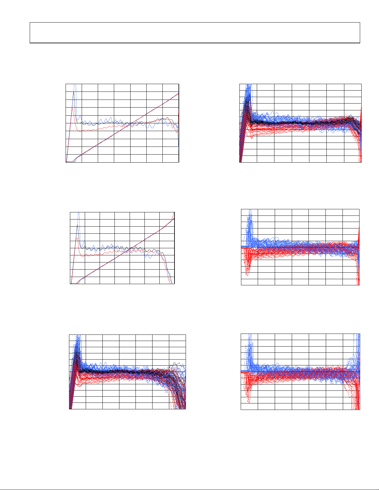
TYPICAL PERFORMANCE CHARACTERISTICS
VS = 5 V, ZO = 50 Ω, Single ended input drive, VOUT tied to VSET, VTGT = 1.4V, CLPF= 3.9 nF, CHPF=2.7 nF, TA = +25°C (Black), –40°C
(Blue), +85°C (red)
4
3.6
3.2
2.8
2.4
2
1.6
1.2
Output Voltage, VOUT (V)
0.8
0.4
0
-60 -50 -40 -30 -20 -10 0 10
Input Amplitude, INHI (dBm)
Figure 3. VOUT Voltage and Log Conformance vs. Input Amplitude at 100 MHz,
Typical Device, TCM1 = 0.47 V, TCM2 = 1.0 V, Sine Wave, -40C, 25C, 85C
2.5
1.5
0.5
-0.5
-1.5
-2.5
3.0
2.0
1.0
Error (dB)
0.0
Error (dB)
-1.0
-2.0
-3.0
-60 -50 -40 -30 -20 -10 0 10
Input Amplitude, INHI (dBm)
Figure 6. Distribution of VOUT Voltage and Error over Temperature After
Ambient Normalization vs. Input Amplitude for at Least 30Devices from
Multiple Lots, Frequency = 100 MHz, TCM1 = 0.47 V, TCM2 = 1.0 V, Sine Wave-
40C, 25C, 85C
4
3.6
3.2
2.8
2.4
2
1.6
1.2
Output Voltage, VOUT (V)
0.8
0.4
0
-60 -50 -40 -30 -20 -10 0 10
Input Amplitude, INHI (dBm)
2.5
1.5
0.5
Error (dB)
-0.5
-1.5
-2.5
Figure 4. VOUT Voltage and Log Conformance vs. Input Amplitude at 900 MHz,
Typical Device, TCM1 = 0.48 V, TCM2 = 1.2 V, Sine Wave -40C, 25C, 85C
3.0
2.0
1.0
0.0
Error (dB)
-1.0
3.0
2.0
1.0
0.0
Error (dB)
-1.0
-2.0
-3.0
-60-50-40-30-20-10 0 10
Input Amplitude, INHI (dBm)
Figure 7. Distribution of Error over Temperature After Ambient Normalization vs.
Input Amplitude, with reference to 25C, for at Least 30Devices from Multiple
Lots, Frequency = 100 MHz, TCM1 = 0.47 V, TCM2 = 1.0 V, Sine Wave-40C, 25C,
85C
3.0
2.0
1.0
0.0
Error (dB)
-1.0
-2.0
-3.0
-60 -50 -40 -30 -20 -10 0 10
Input Amplitude, INHI (dBm)
Figure 5. Distribution of VOUT Voltage and Error over Temperature After
Ambient Normalization vs. Input Amplitude for at Least 30 Devices from
Multiple Lots, Frequency =900 MHz, TCM1 = 0.48 V, TCM2 = 1.2 V, Sine Wave-
40C, 25C, 85C
Rev. PrA | Page 7 of 15
-2.0
-3.0
-60-50-40-30-20-10 0 10
Input Amplitude, INHI (dBm)
Figure 8. Distribution of Error over Temperature After Ambient Normalization vs.
Input Amplitude, with reference to 25C, for at Least 30Devices from Multiple
Lots,, Frequency =900 MHz, TCM1 = 0.48 V, TCM2 = 1.2 V, Sine Wave-40C, 25C,
85C
Page 8

AD8363 Preliminary Technical Data
3.0
3.0
2.0
1.0
0.0
Error (dB)
-1.0
-2.0
-3.0
-60 -50 -40 -30 -20 -10 0
Input Amplitude, INHI (dBm)
Figure 9. VOUT Voltage and Log Conformance vs. Input Amplitude at 1.90 GHz,
Typical Device, TCM1 = 0.51 V, TCM2 = 0.51 V, Sine Wave, -40C, 25C, 85C
3.0
2.0
1.0
0.0
Error (dB)
-1.0
2.0
1.0
0.0
Error (dB)
-1.0
-2.0
-3.0
-60 -50 -40 -30 -20 -10 0
Input Amplitude, INHI (dBm)
Figure 12. Distribution of VOUT Voltage and Error over Temperature After
Ambient Normalization vs. Input Amplitude for at Least 18Devices from
Multiple Lots, Frequency = 1.9 GHz, TCM1 = 0.51 V, TCM2 = 0.51 V, Sine Wave-
40C, 25C, 85C
3.0
2.0
1.0
0.0
Error (dB)
-1.0
-2.0
-3.0
-60 -50 -40 -30 -20 -10 0 10
Input Amplitude, INHI (dBm)
Figure 10. VOUT Voltage and Log Conformance vs. Input Amplitude at 2.14 GHz,
Typical Device, TCM1 = 0.49 V, TCM2 = 1.2 V, Sine Wave, -40C, 25C, 85C
3.0
2.0
1.0
0.0
Error (dB)
-1.0
-2.0
-3.0
-60 -50 -40 -30 -20 -10 0 10
Input Amplitude, INHI (dBm)
Figure 11. Distribution of VOUT Voltage and Error over Temperature After
Ambient Normalization vs. Input Amplitude for at Least 18Devices from
Multiple Lots, Frequency = 2.14 GHz, TCM1 = 0.49 V, TCM2 = 1.2 V, Sine Wave-
40C, 25C, 85C
-2.0
-3.0
-60 -50 -40 -30 -20 -10 0
Input Amplitude, INHI (dBm)
Figure 13. Distribution of Error over Temperature After Ambient Normalization
vs. Input Amplitude, with reference to 25C, for at Least 18 Devices from Multiple
Lots, Frequency = 1.9 GHz, TCM1 = 0.51 V, TCM2 = 0.51 V, Sine Wave-40C, 25C,
85C
3.0
2.0
1.0
0.0
Error (dB)
-1.0
-2.0
-3.0
-60 -50 -40 -30 -20 -10 0 10
Input Amplitude, INHI (dBm)
Figure 14. Distribution of Error over Temperature After Ambient Normalization
vs. Input Amplitude, with reference to 25C, for at Least 18 Devices from Multiple
Lots, Frequency = 2.14 GHz, TCM1 = 0.49 V, TCM2 = 1.2 V, Sine Wave-40C, 25C,
85C
Rev. PrA | Page 8 of 15
Page 9

Preliminary Technical Data AD8363
4
3.6
3.2
2.8
2.4
2
1.6
1.2
Output Voltage, VOUT (V)
0.8
0.4
0
-55 -50 -45 -40 -35 -30 -25 -20 -15 -10 -5 0 5
Input Amplitude, INHI (dBm)
Figure 15. VOUT Voltage and Log Conformance vs. Input Amplitude at 2.6 GHz,
Typical Device, TADJ = TBD V, Sine Wave-40C, 25C, 85C
2.5
1.5
0.5
-0.5
-1.5
-2.5
3.0
2.0
1.0
Error (dB)
0.0
Error (dB)
-1.0
-2.0
-3.0
-55 -50 -45 -40 -35 -30 -25 -20 -15 -10 -5 0 5
Input Amplitude, INHI ( dBm)
Figure 18. Distribution of VOUT Voltage and Error over Temperature After
Ambient Normalization vs. Input Amplitude for at Least 17 Devices from
Multiple Lots, Frequency = 2.6 GHz, TCM1 = 0.52 V, TCM2 = 1.1 V, Sine Wave-
40C, 25C, 85C
4
3.6
3.2
2.8
2.4
2
1.6
1.2
Output Voltage, VOUT (V)
0.8
0.4
0
-55 -50 -45 -40 -35 -30 -25 -20 -15 -10 -5
Input Amplitude, INHI (dBm)
2.5
1.5
0.5
-0.5
-1.5
-2.5
Error (dB)
Figure 16. VOUT Voltage and Log Conformance vs. Input Amplitude at 3.8 GHz,
Typical Device, TCM1 = 0.56 V, TCM2 = 1.0 V, Sine Wave-40C, 25C, 85C
3.0
2.0
1.0
0.0
Error (dB)
-1.0
3.0
2.5
2.0
1.5
1.0
0.5
0.0
-0.5
-1.0
Output Voltage, VOUT (V)
-1.5
-2.0
-2.5
-3.0
-55 -50 -45 -40 -35 -30 -25 -20 -15 -10 -5 0 5
Input Amplitude, INHI (dBm)
Figure 19. Distribution of Error over Temperature After Ambient Normalization
vs. Input Amplitude, with reference to 25C, for at Least 17 Devices from Multiple
Lots, Frequency = 2.6 GHz, TCM1 = 0.52 V, TCM2 = 1.1 V, Sine Wave-40C, 25C,
85C
3.0
2.0
1.0
0.0
Error (dB)
-1.0
-2.0
-3.0
-55 -50 -45 -40 -35 -30 -25 -20 -15 -10 -5
Input Amplitude, INHI (dBm)
Figure 17. Distribution of VOUT Voltage and Error over Temperature After
Ambient Normalization vs. Input Amplitude for at Least 37 Devices from
Multiple Lots, Frequency = 3.8 GHz, TCM1 = 0.56 V, TCM2 = 1.0 V, Sine Wave-
40C, 25C, 85C
Rev. PrA | Page 9 of 15
-2.0
-3.0
-55 -50 -45 -40 -35 -30 -25 -20 -15 -10 -5
Input Amplitude, INHI (dBm)
Figure 20. Distribution of Error over Temperature After Ambient Normalization
vs. Input Amplitude, with reference to 25C, for at Least 37 Devices from Multiple
Lots, Frequency = 3.8 GHz, TCM1 = 0.56 V, TCM2 = 1.0 V, Sine Wave-40C, 25C,
85C
Page 10

AD8363 Preliminary Technical Data
4
3.6
3.2
2.8
2.4
2
1.6
1.2
Output Voltage, VOUT (V)
0.8
0.4
0
-55 -50 -45 -40 -35 -30 -25 -20 -15 - 10 -5
Input Amplitude, INHI (dBm)
Figure 21. VOUT Voltage and Log Conformance vs. Input Amplitude at 5.8 GHz,
Typical Device, TCM1 = 0.88 V, TCM2 = 1.0 V, Sine Wave-40C, 25C, 85C
3
2.5
2
1.5
1
0.5
0
Vout (v)
-0.5
-1
-1.5
-2
-2.5
-3
-60 -50 -40 -30 -20 -10 0 10
Pin (dBm)
Figure 22. Error from CW Linear Reference vs. Input Amplitude with Different
Waveforms, 256 QAM, QPSK, Frequency 2140 MHz
3.50
3.00
2.50
2.00
1.50
1.00
Output Voltage, VOUT (V)
0.50
0.00
-0.50
-4.00E-05
-2.00E-05
0.00E+00
2.00E-05
4.00E-05
6.00E-05
8.00E-05
1.00E-04
1.20E-04
1.40E-04
1.60E-04
1.80E-04
2.00E-04
2.20E-04
2.5
1.5
0.5
3.0
2.0
1.0
0.0
-0.5
Error (dB)
Error (dB)
-1.0
-1.5
-2.5
-2.0
-3.0
-55-50-45-40-35-30-25-20-15-10 -5
Input Amplitude, INHI (dBm)
Figure 24. Distribution of VOUT Voltage and Error over Temperature After
Ambient Normalization vs. Input Amplitude for at Least 37 Devices from
Multiple Lots, Frequency = 5.8 GHz, TCM1 = 0.88 V, TCM2 = 1.0 V, Sine Wave-
40C, 25C, 85C
3.0
2.0
1.0
CW Error
Error 256 QAM
Error QPSK
0.0
Error (dB)
-1.0
-2.0
-3.0
-55 -50 -45 -40 -35 -30 -25 -20 -15 -10 -5
Input Amplitude, INHI (dBm)
Figure 25. Distribution of Error over Temperature After Ambient Normalization
vs. Input Amplitude, with reference to 25C, for at Least 37 Devices from Multiple
Lots, Frequency = 5.8 GHz, TCM1 = 0.88 V, TCM2 = 1.0 V, Sine Wave-40C, 25C,
85C
7.00
6.00
5.00
4.00
3.00
2.00
Output Voltage, VOUT (V)
1.00
0.00
-1.00
2.40E-04
2.60E-04
2.80E-04
3.00E-04
4.00E-04
TCM2 Low
4.40E-04
4.80E-04
5.20E-04
5.60E-04
6.00E-04
6.40E-04
6.80E-04
7.20E-04
7.60E-04
8.00E-04
TCM2 High
8.40E-04
8.80E-04
9.20E-04
9.60E-04
1.00E-03
1.04E-03
1.08E-03
8.00
5.00
2.00
-1.00
-4.00
-7.00
Pulse Voltage, TCM2 (V)
-10.00
-13.00
-16.00
1.12E-03
P_INHI = 0dbm P_INHI = -10dbm P_INHI = -20dbm P_INHI = -30dbm P_INHI = -40dbm
Time (in seconds)
Figure 23. Output Response to RF Burst Input for Various RF Input Levels, Carrier
Frequency 2.14 GHz, CLPF = 470 pF, CHPF=220pF
Rev. PrA | Page 10 of 15
P_INHI = 0dbm P_INHI = -10dbm P_INHI = -20dbm P_INHI = -30dbm
P_INHI = -40dbm P_INHI = -50dbm Pulse on TCM2 (pin1)
Time (in Seconds)
Figure 26. Output Response Using Power-Down Mode for Various RF Input
Levels, Carrier Frequency 2.14 GHz, CLPF= 470pF, CHPF = 220pF
Page 11

Preliminary Technical Data AD8363
Table 4. Pin Function Descriptions
Component Function/Notes Default Value
C12C, C11C,
C6C, C10C, T1C
Input:
The AD8363 was designed to be driven single ended but the dynamic range can be
increased at higher frequencies, if a balun is used. C11C and C12C are used when driving
the AD8363 single ended. C11C and C12C should be removed and 0.1uF capacitors
should be used for C10C and C6C
C12C=0.1uF, C11C=0.1uF,
C6C=Open, C10C=Open,
T1C=AD8363ACPZ-R7
R11C, R10C VTGT:
R10C and R11C are set up to provide 1.4V to VTGT. An external voltage can be used if
R10C and R11C are removed.
C2C, R3C, C5C,
C4C, R1, C1
R6C, R2C, R1C Output Interface--Measurement Mode:
Output Interface--Measurement Mode:
C9C, C8C, R5C Low-pass filter capacitors:
C3C CHPF capacitor
Power Supply Decoupling:
The nominal supply decoupling consists of a 100 pF filter capacitor placed physically
close to the AD8363, a 0 Ω series resistor, and a 0.1 uF capacitor placed closer to the
power supply input pin.
In measurement mode, a portion of the output voltage is fed back to the VSET pin via
R6C. The magnitude of the slope at VPUT can be increased by reducing the portion of
V
that is fed back to VSET. If a fast responding output is expected, the 0 Ω resistor on
OUT
R1C can be removed to reduce parasitics on the output.
In this mode, R6C must be open and R2C must have a 0 Ω resistor. In controller mode,
the AD8363 can control the gain of an external component. A setpoint voltage is applied
to the VSET pin, the value of which corresponds to the desired RF input signal level
applied to the AD8363 RF input. If a fast responding output is expected, the 0 Ω resistor
on R1C can be removed to reduce parasitics on the output.
The low-pass filter capacitors reduce the noise on the output and affect the pulse
response time of the AD8363. The smallest CLPF capacitance should be 400 pF
The CHPF capacitor introduces a high-pass filter effect into the AD8363 transfer function
and can affect the response time. It should be tied to VPOS.
R10C=845Ω, R11C= 1.4KΩ
C2C=0.1uF, R3C=0 Ω,
C5C=100 pF, C4C= 100 pF,
R1= 0 Ω, C1=0.1uF
R6C=0 Ω, R2C=Open, R1C=0
Ω
C9C=0.1uF, C8C=Open,
R5C=0 Ω
C3C= 0.1uF
C1C, R9C, R4C ENT2/PWDN:
The ENT2/PWDN pin controls the amount of nonlinear intercept temperature
compensation and/or shuts down the device. The evaluation board is configured to
control this from a test loop but VREF can be used through a voltage divider created from
R9C and R4C.
R2, R3 TCM1:
TCM1 controls the intercept temperature compensation (3K impedance). The evaluation
board is configured to control this from a test loop but VREF can be used through a
voltage divider created from R2 and R3
C1C=Open, R9C= Open,
R4C= Open
R2=Open, R3=Open
Rev. PrA | Page 11 of 15
Page 12

AD8363 Preliminary Technical Data
A
C
EVALUATION BOARD
C2C
0.1UF
AGNDC
8
567
C4C
C0402
100PF
0.1UF
VPOS
C0402
AGNDC
C1
C0402
AGNDC
TEMPC
C9C
AGNDC
C0402
R5C
R0402
TESTLOOP
WHITE
0.1UF
0
AGNDC
R6C
R0402
0
AGNDC
DNIR2C
R0402
OPEN
50 ohm Impedance
R1C
0
R0402
VOUTC
C8C
OPEN
C0402
VSETC
VIOLET
1
SMASMT
TESTLOOP
YELLOW
AGNDC;3 4 5
AGNDC;3 4 5
RFINB
2
AGNDC
RFIN
2
AGNDC
GNDC
50 ohm Impedance
1
SMASMT
AGNDC
1
5
2
1
SMASMT
TESTLOOP
BLACK
AGNDC
R11C
AGNDC
T1C
4
3
AGNDC
SHDN_TADJC
TESTLOOP
ORANGE
TESTLOOP
ORANGE
VREFC
R3C
0
R0402
1.4K
TESTLOOP
ORANGE
R0402
VTGTC
R10C
845
R0402
VREFC
C5C
C0402
100PF
0.1UF
C11C
AGNDC
C10C
OPEN
C6C
OPEN
C0402
131416 15
C0402
C0402
NCON
INHI
INLO
TCM1
12
VTGT
11 9
10
VPOS
VREF
DUT1C
16CSP4X4
AD8363
COMM
TEMP
VSET
VOUT
CLPF
0.1UF
C0402
C12C
TC1
TESTLOOP
White
R3
OPEN
R0402
R9C
R0402 R0402
VREFC
R4C
OpenOpen
AGNDC
R2
OPEN
R0402
C1C
OPEN
C0402
AGNDC
VREFC
CHPF
ENT2
13
2
VPOS
COMM
4
AGNDC
C3C
C0402
0.1UF
VPOSC
RED
TESTLOOP
VPOSC
R1
0
R0402
TESTLOOP
VOUT
AGNDC
2
GNDC;3 4 5
Rev. PrA | Page 12 of 15
Page 13

Preliminary Technical Data AD8363
ASSEMBLY DRAWINGS
Rev. PrA | Page 13 of 15
Page 14

AD8363 Preliminary Technical Data
Rev. PrA | Page 14 of 15
Page 15

Preliminary Technical Data AD8363
OUTLINE DIMENSIONS
4.00
PIN 1
INDICATO
1.00
0.85
0.80
R
12° MAX
SEATING
PLANE
BSC SQ
TOP
VIEW
BSC SQ
0.80 MAX
0.65 TYP
0.30
0.20 REF
0.23
0.18
COMPLIANT TO JEDEC STANDARDS MO-220-VGGC
3.75
0.60 MAX
0.65 BSC
0.05 MAX
0.02 NOM
COPLANARITY
0.75
0.60
0.50
0.08
ORDERING GUIDE
Model Temperature Range Package Description Package Option Ordering Quantity
AD8363ACPZ-R7
AD8363ACPZ-R2 40°C to +125°C 16-Lead Lead Frame Chip Scale Package [LFCSP_VQ] CP-16-4 250
40°C to +125°C
16-Lead Lead Frame Chip Scale Package [LFCSP_VQ] CP-16-4
0.60 MAX
13
12
EXPOSED
(BOTTOM VIEW)
9
8
PAD
16
1
4
5
1.95 BSC
PIN 1
INDICATOR
2.25
2.10 SQ
1.95
0.25 MIN
1500
AD8363ACPZ-WP 40°C to +125°C 16-Lead Lead Frame Chip Scale Package [LFCSP_VQ] CP-16-4 64
AD8363-EVALZ Evaluation Board
Rev. PrA | Page 15 of 15 PR07368-0-2/08(PrA)
 Loading...