

Page 1
2.9 GHz Ultralow Distortion
V
V
V
FEATURES
−3 dB bandwidth of 2.9 GHz (AV = 6 dB)
Low supply current: 40 mA
Pin-strappable gain adjust: 6 dB, 12 dB, 15.5 dB
Differential or single-ended input to differential output
Low noise input stage: 2.1 nV/√Hz RTI at A
Low broadband distortion (Av = 6 dB)
10 MHz: −94 dBc HD2, −87 dBc HD3
70 MHz: −98 dBc HD2, −87 dBc HD3
140 MHz: −95 dBc HD2, −87 dBc HD3
250 MHz: −80 dBc HD2, −73 dBc HD3
IMD3s of −86 dBc @ 250 MHz center
Slew rate: 9.8 V/ns
Fast settling of 2 ns and overdrive recovery of 3 ns
Single-supply operation: 3 V to 3.6 V
Power-down control
Fabricated using the high speed XFCB3 SiGe process
APPLICATIONS
Differential ADC drivers
Single-ended-to-differential conversion
RF/IF gain blocks
SAW filter interfacing
= 12 dB
V
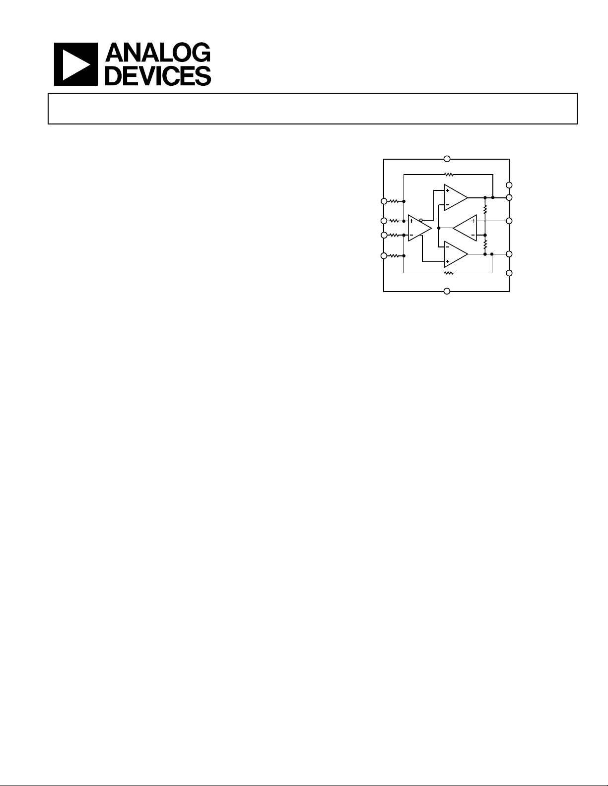
RF/IF Differential Amplifier
ADL5561
FUNCTIONAL BLOCK DIAGRAM
CC
R
F
ENBL
VON
VCOM
VOP
GND
08004-001
VIP2
VIP1
IN1
IN2
R
G2
R
G1
R
G1
R
G2
R
F
ADL5561
GND
Figure 1.
GENERAL DESCRIPTION
The ADL5561 is a high performance differential amplifier
optimized for RF and IF applications. The amplifier offers low
noise of 2.1 nV/√Hz and excellent distortion performance over
a wide frequency range, making it an ideal driver for high speed
8-bit to 16-bit analog-to-digital converters (ADCs).
The ADL5561 provides three gain levels of 6 dB, 12 dB, and 15.5 dB
through a pin-strappable configuration. For the single-ended
input configuration, the gains are reduced to 5.6 dB, 11.1 dB, and
14.1 dB. Using an external series input resistor expands the
amplifier gain flexibility and allows for any gain selection from
0 dB to 15.5 dB.
The quiescent current of the ADL5561 is typically 40 mA and,
when disabled, consumes less than 3 mA, offering excellent
input-to-output isolation.
Rev. C
Information furnished by Analog Devices is believed to be accurate and reliable. However, no
responsibility is assumed by Anal og Devices for its use, nor for any infringements of patents or ot her
rights of third parties that may result from its use. Specifications subject to change without notice. No
license is granted by implication or otherwise under any patent or patent rights of Analog Devices.
Trademarks and registered trademarks are the property of their respective owners.
The device is optimized for wideband, low distortion performance.
These attributes, together with its adjustable gain capability,
make this device the amplifier of choice for general-purpose IF
and broadband applications where low distortion, noise, and power
are critical. This device is optimized for the best combination of
slew speed, bandwidth, and broadband distortion. These attributes
allow it to drive a wide variety of ADCs and make it ideally suited
for driving mixers, pin diode attenuators, SAW filters, and multielement discrete devices.
Fabricated on the Analog Devices, Inc., high speed SiGe process,
the ADL5561 is supplied in a compact 3 mm × 3 mm, 16-lead
LFCSP package and operates over the temperature range of
−40°C to +85°C.
One Technology Way, P.O. Box 9106, Norwood, MA 02062-9106, U.S.A.
Tel: 781.329.4700 www.analog.com
Fax: 781.461.3113 ©2009–2011 Analog Devices, Inc. All rights reserved.
Page 2

ADL5561
TABLE OF CONTENTS
Features.............................................................................................. 1
Applications....................................................................................... 1
Functional Block Diagram ..............................................................1
General Description......................................................................... 1
Revision History ...............................................................................2
Specifications..................................................................................... 3
Absolute Maximum Ratings............................................................ 6
ESD Caution.................................................................................. 6
Pin Configuration and Function Descriptions............................. 7
Typical Performance Characteristics............................................. 8
Circuit Description......................................................................... 13
Basic Structure............................................................................ 13
REVISION HISTORY
6/11—Rev. B to Rev. C
Changes to Figure 28 and Figure 29............................................. 12
Added Figure 30 and Figure 31; Renumbered Sequentially .....12
Changes to Ordering Guide.......................................................... 21
3/10—Rev A to Rev. B
Changes to Figure 43...................................................................... 21
Changes to Ordering Guide.......................................................... 21
9/09—Rev 0 to Rev. A
Changes to Features Section............................................................ 1
Changes to Table 1............................................................................ 3
Changes to Figure 5.......................................................................... 8
Changes to Figure 9 and Figure 10................................................. 9
Changes to Equation 1, Figure 32, and Figure 34....................... 15
Changes to Equation 2................................................................... 16
Changes to Figure 38, Figure 39, Figure 40, and Table 9........... 17
Changes to Figure 43...................................................................... 19
Moved Table 14 to ......................................................................... 19
5/09—Revision 0: Initial Version
Applications Information.............................................................. 14
Basic Connections...................................................................... 14
Input and Output Interfacing................................................... 15
Gain Adjustment and Interfacing ............................................ 16
ADC Interfacing......................................................................... 16
Layout Considerations............................................................... 18
Soldering Information............................................................... 19
Evaluation Board........................................................................ 19
Outline Dimensions....................................................................... 21
Ordering Guide .......................................................................... 21
Rev. C | Page 2 of 24
Page 3

ADL5561
SPECIFICATIONS
VCC = 3.3 V, VCOM = 1.65 V, RL = 200 Ω differential, AV = 6 dB, CL = 1 pF differential, f = 140 MHz, TA = 25°C.
Table 1.
Parameter Conditions Min Typ Max Unit
DYNAMIC PERFORMANCE
−3 dB Bandwidth AV = 6 dB, V
A
A
= 12 dB, V
V
= 15.5 dB, V
V
Bandwidth for 0.1 dB Flatness AV = 6 dB, V
A
A
= 12 dB, V
V
= 15.5 dB, V
V
Gain Accuracy AV = 6 dB, RL = open 0.15 dB
A
A
= 12 dB, RL = open 0.05 dB
V
= 15.5 dB, RL = open 0.05 dB
V
Gain Supply Sensitivity VCC ± 10% −0.023 dB/V
Gain Temperature Sensitivity −40°C to +85°C, AV =15.5 dB 0.24 mdB/°C
Slew Rate Rise, AV = 15.5 dB, RL= 200 Ω, V
Fall, AV = 15.5 dB, RL = 200 Ω, V
Settling Time 2 V step to 1% 2 ns
Overdrive Recovery Time VIN = 4 V to 0 V step, V
Reverse Isolation (S12) 60 dB
INPUT/OUTPUT CHARACTERISTICS
Output Common Mode VCC/2 V
Voltage Adjustment Range 1.4 to 1.8 V
Maximum Output Voltage Swing 1 dB compressed 4.3 V p-p
Output Common-Mode Offset Referenced to VCC/2 25 mV
Output Common-Mode Drift −40°C to +85°C 170 μV/°C
Output Differential Offset Voltage 1 mV
CMRR 65 dB
Output Differential Offset Drift −40°C to +85°C 15 μV/°C
Input Bias Current 3 μA
Input Resistance (Differential) AV = 6 dB 400 Ω
A
A
Input Resistance (Single-Ended)1 A
A
A
= 12 dB 200 Ω
V
= 15.5 dB 133 Ω
V
= 5.6 dB, RS = 50 Ω 307 Ω
V
= 11.1 dB, RS = 50 Ω 179 Ω
V
= 14.1 dB, RS = 50 Ω 132 Ω
V
Input Capacitance (Single-Ended) 0.3 pF
Output Resistance (Differential) 12 Ω
POWER INTERFACE
Supply Voltage 3 3.3 3.6 V
ENBL Threshold Device disabled, ENBL low 0.6 V
Device enabled, ENBL high 1.3 V
ENBL Input Bias Current ENBL high −27 μA
ENBL low −300 μA
Quiescent Current ENBL high 37 40 44.5 mA
ENBL low 3 mA
≤ 1.0 V p-p 2900 MHz
OUT
≤ 1.0 V p-p 2300 MHz
OUT
≤ 1.0 V p-p 1800 MHz
OUT
≤ 1.0 V p-p 200 MHz
OUT
≤ 1.0 V p-p 200 MHz
OUT
≤ 1.0 V p-p 600 MHz
OUT
= 2 V step 9.8 V/ns
OUT
= 2 V step 10.1 V/ns
OUT
≤ ±10 mV 3 ns
OUT
Rev. C | Page 3 of 24
Page 4

ADL5561
Parameter Conditions Min Typ Max Unit
10 MHz NOISE/HARMONIC PERFORMANCE
Second/Third Harmonic Distortion AV = 6 dB, RL = 200 Ω, V
A
A
Output Third-Order Intercept/Third-Order
Intermodulation Distortion
= 12 dB, RL = 200 Ω, V
V
= 15.5 dB, RL = 200 Ω, V
V
AV= 6 dB, RL = 200 Ω, V
composite (2 MHz spacing)
= 12 dB, RL = 200 Ω, V
A
V
composite (2 MHz spacing)
= 15.5 dB, RL = 200 Ω, V
A
V
composite (2 MHz spacing)
Noise Spectral Density (RTI) AV = 6 dB 3 nV/√Hz
A
A
= 12 dB 2.1 nV/√Hz
V
= 15.5 dB 1.7 nV/√Hz
V
1 dB Compression Point (RTO) AV = 6 dB 19 dBm
A
A
= 12 dB 19 dBm
V
= 15.5 dB 19 dBm
V
70 MHz NOISE/HARMONIC PERFORMANCE
Second/Third Harmonic Distortion AV = 6 dB, RL = 200 Ω, V
A
A
Output Third-Order Intercept/Third-Order
Intermodulation Distortion
= 12 dB, RL = 200 Ω, V
V
= 15.5 dB, RL = 200 Ω, V
V
AV = 6 dB, RL = 200 Ω, V
composite (2 MHz spacing)
= 12 dB, RL = 200 Ω, V
A
V
composite (2 MHz spacing)
= 15.5 dB, RL = 200 Ω, V
A
V
composite (2 MHz spacing)
Noise Spectral Density (RTI) AV = 6 dB 3 nV/√Hz
A
A
= 12 dB 2.1 nV/√Hz
V
= 15.5 dB 1.7 nV/√Hz
V
1 dB Compression Point (RTO) AV = 6 dB 19 dBm
A
A
= 12 dB 18.9 dBm
V
= 15.5 dB 18.9 dBm
V
140 MHz NOISE/HARMONIC PERFORMANCE
Second/Third Harmonic Distortion AV = 6 dB, RL = 200 Ω, V
A
A
Output Third-Order Intercept/Third-Order
Intermodulation Distortion
= 12 dB, RL = 200 Ω, V
V
= 15.5 dB, RL = 200 Ω, V
V
AV = 6 dB, RL = 200 Ω, V
composite (2 MHz spacing)
= 12 dB, RL = 200 Ω, V
A
V
composite (2 MHz spacing)
= 15.5 dB, RL = 200 Ω, V
A
V
composite (2 MHz spacing)
Noise Spectral Density (RTI) AV = 6 dB 3 nV/√Hz
A
A
= 12 dB 2.1 nV/√Hz
V
= 15.5 dB 1.7 nV/√Hz
V
1 dB Compression Point (RTO) AV = 6 dB 19.1 dBm
A
A
= 12 dB 18.8 dBm
V
= 15.5 dB 18.7 dBm
V
= 2 V p-p −94/−87 dBc
OUT
= 2 V p-p −92/−88 dBc
OUT
= 2 V p-p −95/−87 dBc
OUT
= 2 V p-p
OUT
= 2 V p-p
OUT
= 2 V p-p
OUT
= 2 V p-p −98/−87 dBc
OUT
= 2 V p-p −93/−83 dBc
OUT
= 2 V p-p −93/−82 dBc
OUT
= 2 V p-p
OUT
= 2 V p-p
OUT
= 2 V p-p
OUT
= 2 V p-p −95/−87 dBc
OUT
= 2 V p-p −83/−83 dBc
OUT
= 2 V p-p −83/−82 dBc
OUT
= 2 V p-p
OUT
= 2 V p-p
OUT
= 2 V p-p
OUT
+42.7/−89 dBm/dBc
+41/−85 dBm/dBc
+40/−85 dBm/dBc
+45/−93 dBm/dBc
+43/−89 dBm/dBc
+41/−86 dBm/dBc
+49/−102 dBm/dBc
+48/−100 dBm/dBc
+39/−96 dBm/dBc
Rev. C | Page 4 of 24
Page 5

ADL5561
Parameter Conditions Min Typ Max Unit
250 MHz NOISE/HARMONIC PERFORMANCE
Second/Third Harmonic Distortion AV = 6 dB, RL = 200 Ω, V
A
A
Output Third-Order Intercept/Third-Order
Intermodulation Distortion
= 12 dB, RL = 200 Ω, V
V
= 15.5 dB, RL = 200 Ω, V
V
AV = 6 dB, RL = 200 Ω, V
composite (2 MHz spacing)
= 12 dB, RL = 200 Ω, V
A
V
composite (2 MHz spacing)
= 15.5 dB, RL = 200 Ω, V
A
V
composite (2 MHz spacing)
Noise Spectral Density (RTI) AV = 6 dB 3.2 nV/√Hz
A
A
= 12 dB 2.2 nV/√Hz
V
= 15.5 dB 1.7 nV/√Hz
V
1 dB Compression Point (RTO) AV = 6 dB 19.1 dBm
A
A
= 12 dB 18.9 dBm
V
= 15.5 dB 18.7 dBm
V
500 MHz NOISE/HARMONIC PERFORMANCE
Second/Third Harmonic Distortion AV = 6 dB, RL = 200 Ω, V
A
A
Output Third-Order Intercept/Third-Order
Intermodulation Distortion
= 12 dB, RL = 200 Ω, V
V
= 15.5 dB, RL = 200 Ω, V
V
AV = 6 dB, RL = 200 Ω, V
composite (2 MHz spacing)
= 12 dB, RL = 200 Ω, V
A
V
composite( 2 MHz spacing)
= 15.5 dB, RL = 200 Ω, V
A
V
composite (2 MHz spacing)
Noise Spectral Density (RTI) AV = 6 dB 4.1 nV/√Hz
A
A
= 12 dB 2.4 nV/√Hz
V
= 15.5 dB 1.8 nV/√Hz
V
1 dB Compression Point (RTO) AV = 6 dB 16.3 dBm
A
A
= 12 dB 16.4 dBm
V
= 15.5 dB 16.2 dBm
V
1000 MHz NOISE/HARMONIC PERFORMANCE
Second/Third Harmonic Distortion AV = 6 dB, RL = 200 Ω, V
A
A
Output Third-Order Intercept/Third-Order
Intermodulation Distortion
= 12 dB, RL = 200 Ω, V
V
= 15.5 dB, RL = 200 Ω, V
V
AV = 6 dB, RL = 200 Ω, V
composite (2 MHz spacing)
= 12 dB, RL = 200 Ω, V
A
V
composite (2 MHz spacing)
= 15.5 dB, RL = 200 Ω, V
A
V
composite (2 MHz spacing)
Noise Spectral Density (RTI) AV = 6 dB 6 nV/√Hz
A
A
= 12 dB 2.6 nV/√Hz
V
= 15.5 dB 1.8 nV/√Hz
V
1 dB Compression Point (RTO) AV = 6 dB 10.8 dBm
A
A
1
See the section for a discussion of single-ended input, dc-coupled operation. Applications Information
= 12 dB 12.6 dBm
V
= 15.5 dB 12.5 dBm
V
= 2 V p-p −80/−73 dBc
OUT
= 2 V p-p −76/−70 dBc
OUT
= 2 V p-p −78/−72 dBc
OUT
= 2 V p-p
OUT
= 2 V p-p
OUT
= 2 V p-p
OUT
= 1 V p-p −69/−57 dBc
OUT
= 1 V p-p −72/−60 dBc
OUT
= 1V p-p −66/−61 dBc
OUT
= 1 V p-p
OUT
= 1 V p-p
OUT
= 1 V p-p
OUT
= 1 V p-p −58/−53 dBc
OUT
= 1 V p-p −55/−50 dBc
OUT
= 1 V p-p −57/−50 dBc
OUT
= 1 V p-p
OUT
= 1 V p-p
OUT
= 1 V p-p
OUT
+41/−86 dBm/dBc
+40/−84 dBm/dBc
+39/−83 dBm/dBc
+40/−97 dBm/dBc
+36/−90 dBm/dBc
+34/−75 dBm/dBc
+18/−54 dBm/dBc
+18/−56 dBm/dBc
+18/−46 dBm/dBc
Rev. C | Page 5 of 24
Page 6
ADL5561
ABSOLUTE MAXIMUM RATINGS
Table 2.
Parameter Rating
Supply Voltage (VCC) 3.6 V
VIP1, VIP2, VIN1, VIN2 VCC + 0.5 V
Internal Power Dissipation 155 mW
θJA 98.3°C/W
Maximum Junction Temperature 125°C
Operating Temperature Range −40°C to +85°C
Storage Temperature Range −65°C to +150°C
Stresses above those listed under Absolute Maximum Ratings
may cause permanent damage to the device. This is a stress
rating only; functional operation of the device at these or any
other conditions above those indicated in the operational
section of this specification is not implied. Exposure to absolute
maximum rating conditions for extended periods may affect
device reliability.
ESD CAUTION
Rev. C | Page 6 of 24
Page 7
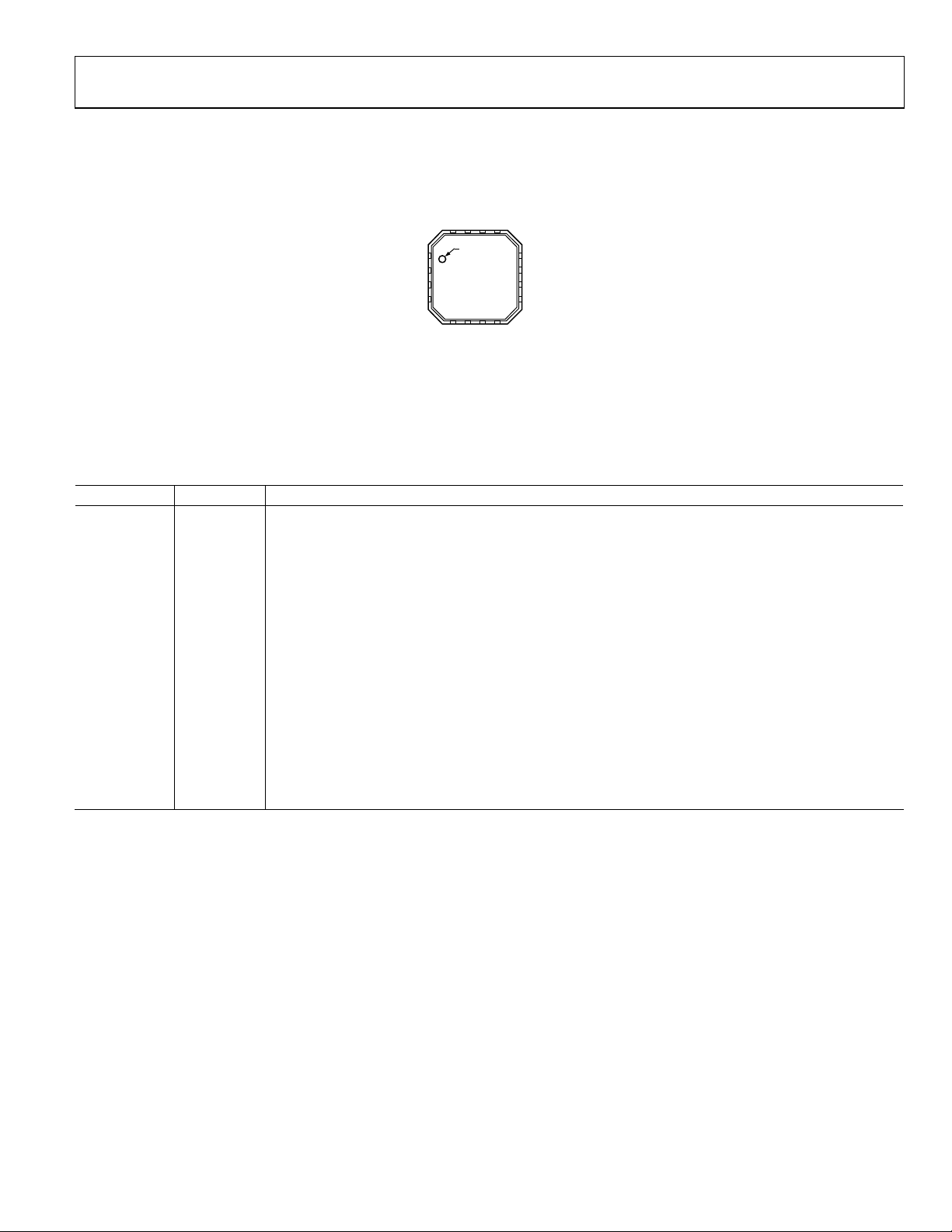
ADL5561
PIN CONFIGURATION AND FUNCTION DESCRIPTIONS
GND
GND
GND
GND
14
13
15
16
PIN 1
INDICATOR
1VIP2
2VIP1
ADL5561
3VIN1
TOP VIEW
(Not to Scale)
4VIN2
5
6
VCC
NOTES
1. EXPOSED P ADDLE. CONNECT TO A LO W
IMPEDANCE THERMAL AND ELECTRI CAL
GROUND PLANE.
VCC
Figure 2. Pin Configuration
Table 3. Pin Function Descriptions
Pin No. Mnemonic Description
1 VIP2
2 VIP1
3 VIN1
4 VIN2
Balanced Differential Input. Biased to VCOM, typically ac-coupled. Input for A
VIP1 for A
= 15.5 dB.
v
Balanced Differential Input. Biased to VCOM, typically ac-coupled. Input for A
VIP2 for A
= 15.5 dB.
v
Balanced Differential Input. Biased to VCOM, typically ac-coupled. Input for A
VIN2 for A
= 15.5 dB.
v
Balanced Differential Input. Biased to VCOM, typically ac-coupled. Input for A
VIN1 for A
= 15.5 dB.
v
5, 6, 7, 8 VCC Positive Supply.
9 VCOM
Common-Mode Voltage. A voltage applied to this pin sets the common-mode voltage of the input and
output. Typically decoupled to ground with a 0.1 μF capacitor. With no reference applied, input and
output common mode floats to midsupply (VCC/2).
10 VON Balanced Differential Output. Biased to VCOM, typically ac-coupled.
11 VOP Balanced Differential Output. Biased to VCOM, typically ac-coupled.
12 ENBL Enable. Apply positive voltage (1.0 V < ENBL < VCC) to activate device.
13, 14, 15, 16 GND Ground. Connect to low impedance ground.
EP Exposed Paddle. Connect to a low impedance thermal and electrical ground plane.
12 ENBL
11 VOP
10 VON
9VCOM
8
7
VCC
VCC
08004-031
= 12 dB gain, strapped to
V
= 6 dB gain, strapped to
V
= 6 dB gain, strapped to
V
= 12 dB gain, strapped to
V
Rev. C | Page 7 of 24
Page 8
ADL5561
T
√
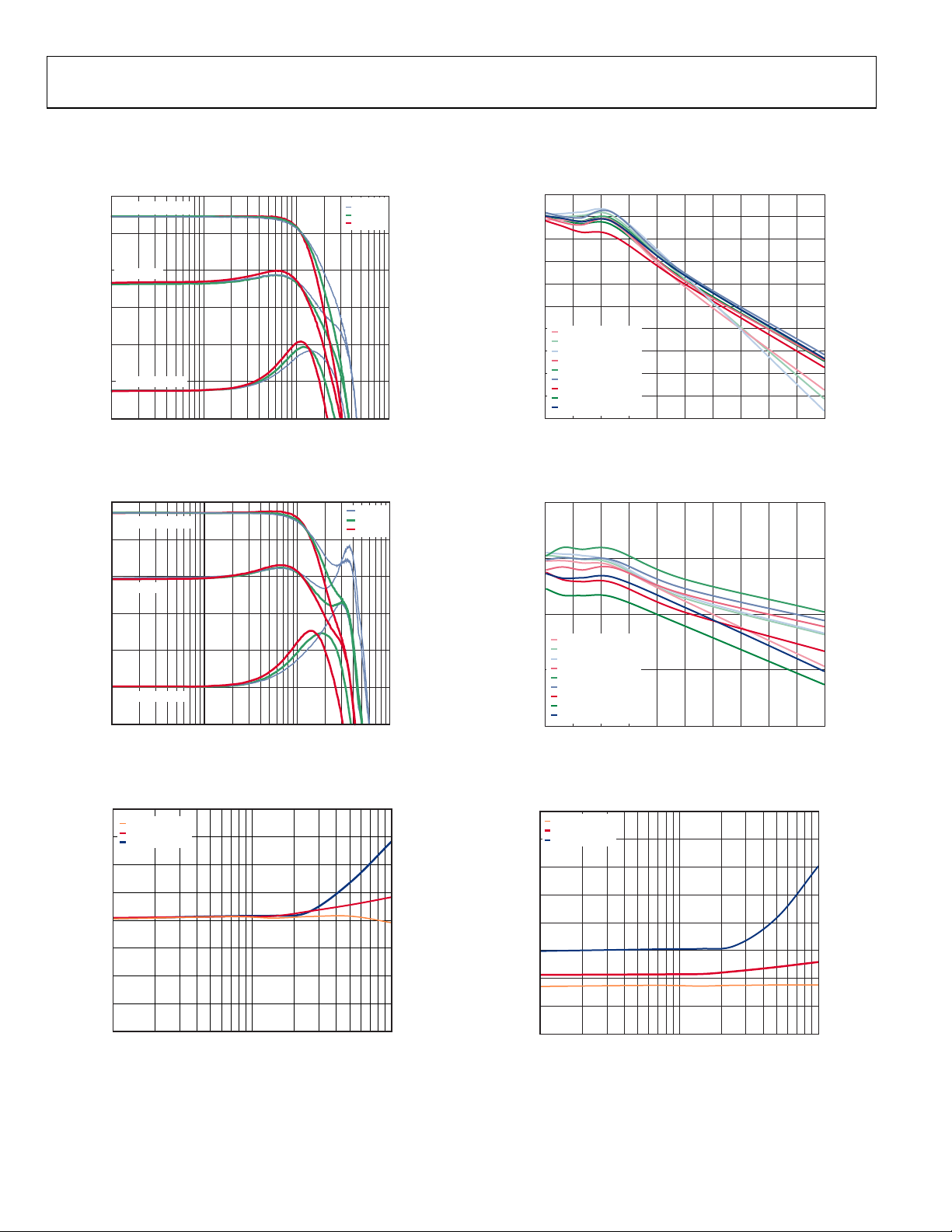
TYPICAL PERFORMANCE CHARACTERISTICS
VCC = 3.3 V, VCOM = 1.65 V, RL = 200 Ω differential, AV = 6 dB, CL = 1 pF differential, f = 140 MHz, and TA = 25°C.
16
MAXIMUM GAIN
14
12
MID GAIN
10
GAIN (dB)
8
6
MINIMUM GAIN
4
10M 100M 1G 10G
FREQUENCY ( Hz)
–40°C
+25°C
+85°C
Figure 3. Gain vs. Frequency Response for 200 Ω Differential Load,
= 6 dB, AV = 12 dB, and AV = 15.5 dB over Temperature
A
V
16
MAXIMUM GAIN
14
12
MID GAIN
10
GAIN (dB)
8
6
MINIMUM GAIN
4
10M 100M 1G 10G
FREQUENCY ( Hz)
–40°C
+25°C
+85°C
Figure 4. Gain vs. Frequency Response for 1 kΩ Differential Load
= 6 dB, AV = 12 dB, and AV = 15.5 dB over Temperature
A
V
16
AV MAXIMUM
A
MID
V
14
A
MINIMUM
V
12
10
8
6
NOISE FI GURE (dB)
4
2
0
10 100 1000
FREQUE NCY (MHz)
Figure 5. Noise Figure vs. Frequency at
= 6 dB, AV = 12 dB, and AV = 15.5 dB
A
V
08004-002
08004-003
08004-004
20
19
18
17
16
15
14
MIN GAIN +85°C
OP1dB (dBm)
MIN GAIN +25°C
MIN GAIN –40°C
13
MID GAIN +85°C
MID GAIN +25°C
12
MID GAIN –40°C
MAX GAIN +85°C
11
MAX GAIN +25°C
MAX GAIN –40°C
10
0 100 200 300 400 500 600 700 800 900 1000
FREQUENCY ( MHz)
Figure 6. Output P1dB (OP1dB) vs. Frequency at A
= 15.5 dB over Temperature, 200 Ω Differential Load
A
V
25
20
15
MIN GAIN +85°C
OP1dB (dBm)
MIN GAIN +25°C
MIN GAIN –40°C
MID GAIN +85°C
10
MID GAIN +25°C
MID GAIN –40°C
MAX GAIN +85°C
MAX GAIN +25°C
MAX GAIN –40°C
5
0 100 200 300 400 500 600 700 800 900 1000
FREQUENCY ( MHz)
Figure 7. Output P1dB (OP1dB) vs. Frequency at A
= 15.5 dB over Temperature, 1 kΩ Differential Load
A
V
8
AV MAXIMUM
A
MID
V
7
A
MINIMUM
Hz)
Y (nV/
NOISE SPECT RAL DENSI
V
6
5
4
3
2
1
0
10 100 1000
FREQUENCY ( MHz)
V
V
Figure 8. Noise Spectral Density vs. Frequency at
= 6 dB, AV = 12 dB, and AV = 15.5 dB
A
V
08004-016
= 6 dB, AV = 12 dB, and
08004-017
= 6 dB, AV = 12 dB, and
08004-015
Rev. C | Page 8 of 24
Page 9

ADL5561
R
–
60
50
AV MAXIMUM
A
MID
V
A
MINIMUM
V
–40
–60
AV MAXIMUM
A
MID
V
A
MINIMUM
V
0
–20
40
30
OIP3 (dBm)
20
10
0
0 50 100 150 200 250
FREQUENCY (MHz)
08004-018
Figure 9. Output Third-Order Intercept at Three Gains, Output Level at 2 V p-p
Composite, R
60
+85°C MAX GAIN
+25°C MAX GAIN
–40°C MAX GAI N
50
40
30
OIP3 (dBm)
20
10
0
0 50 100 150 200 250
FREQUENCY (MHz)
= 200 Ω
L
08004-019
Figure 10. Output Third-Order Intercept vs. Frequency, Over Temperature,
Output Level at 2 V p-p Composite, R
60
AV MAXIMUM
A
MID
V
A
MINIMUM
V
55
50
45
OIP3 (dBm)
40
35
30
0 50 100 150 200 250
FREQUE NCY (MHz)
= 200 Ω
L
08004-005
Figure 11. OIP3 vs. Frequency (Single-Ended Input)
–80
–100
= 200Ω (dBc)
L
–120
IMD3,
–140
–160
0 50 100 150 200 250
FREQUENCY ( MHz)
Figure 12. Two-Tone Output IMD vs. Frequency,
Output Level at 2 V p-p Composite, R
50
45
40
35
30
25
20
OIP3 (dBm)
15
10
5
0
–2 –1 0 1 2 3 4 5
P
/TONE (dBm)
OUT
= 200 Ω and RL = 1 kΩ
L
Figure 13. Output Third-Order Intercept (OIP3) vs. Power (P
Frequency 140 MHz, A
70
AV MAXIMUM
A
MID
V
–75
A
MINIMUM
V
–80
–85
–90
IMD (dBc)
–95
–100
–105
–110
0 50 100 150 200 250
FREQUENCY (MHz )
= 15.5 dB
V
Figure 14. IMD vs. Frequency (Single-Ended Input)
OUT
–40
–60
–80
–100
–120
),
= 1kΩ (dBc)
L
IMD3, R
08004-020
08004-021
08004-006
Rev. C | Page 9 of 24
Page 10

ADL5561
–
–
–
–
–
–40
–60
–80
–100
–120
–140
HARMONIC DIS TORTION HD2 (dBc)
–160
0 50 100 150 200 250
FREQUENCY ( MHz)
AV MAXIMUM
A
V
A
V
Figure 15. Harmonic Distortion (HD2/HD3) vs. Frequency at A
= 12 dB, and AV = 15.5 dB, Output Level at 2 V p-p, RL = 200 Ω
A
V
40
–60
–80
–100
–120
–140
HARMONIC DIS TORTIO N HD2 (dBc)
MID
MINIMUM
+85°C
+25°C
–40°C
0
–20
–40
–60
–80
–100
–120
= 6 dB,
V
0
–20
–40
–60
–80
–100
HARMONIC DIS TORTION HD3 ( dBc)
HARMONIC DIS TORTION HD3 (dBc)
40
AV MAXIMUM
A
MID
V
A
MINIMUM
V
–60
–80
–100
–120
–140
HARMONIC DIS TORTIO N HD2 (dBc)
–160
0 50 100 150 200 250
08004-022
Figure 18. Harmonic Distortion (HD2/HD3) vs. Frequency at A
= 12 dB, and AV = 15.5 dB, Output Level at 2 V p-p, RL = 1 k Ω
A
V
20
–30
–40
–50
–60
–70
–80
HARMONIC DIS TORTION (dBc)
–90
FREQUENCY (MHz)
HD2
HD3
0
–20
–40
–60
–80
–100
–120
= 6 dB,
V
HARMONIC DIS TORTION HD3 (dBc)
08004-026
–160
0 50 100 150 200 250
FREQUENCY ( MHz)
–120
Figure 16. Harmonic Distortion (HD2/HD3) vs. Frequency,
Three Temperatures, Output Level at 2 V p-p, R
40
–60
–80
–100
–120
–140
HARMONIC DIS TORTION HD2 (d Bc)
–160
0 50 100 150 200 250
FREQUENCY (MHz)
= 200 Ω
L
+85°C
+25°C
–40°C
0
–20
–40
–60
–80
–100
–120
HARMONIC DIS TORTION HD3 (dBc)
Figure 17. Harmonic Distortion (HD2/HD3) vs. Frequency, Over Temperature,
Output Level at 2 V p-p, R
= 1 kΩ
L
–100
–2–1012345
(dBm)
08004-024
P
OUT
08004-023
Figure 19. Harmonic Distortion (HD2/HD3) vs. Power, Frequency 140 MHz,
= 15.5 dB
A
V
60
AV MAXIMUM
A
–65
–70
–75
–80
–85
–90
–95
–100
HARMONIC DISTORTION HD2 (d Bc)
–105
–110
08004-025
MID
V
A
MINIMUM
V
0 50 100 150 200 250
FREQUENCY ( MHz)
0
–10
–20
–30
–40
–50
–60
–70
–80
–90
–100
HARMONIC DISTORTION HD3 (d Bc)
08004-007
Figure 20. Ha rmonic Distortion (HD2/HD3) vs. Frequency (Single-Ended Input)
Rev. C | Page 10 of 24
Page 11

ADL5561
–
–
–
–
L
A
30
–40
–50
–60
–70
–80
HARMONIC DIS TORTION HD2 (dBc)
–90
–100
0 100 200 300 400 500 600 700 800 900 1k
R
LOAD
(Ω)
AV MAXIMUM
A
A
Figure 21. Harmonic Distortion (HD2/HD3) vs. R
ENABLE
VOLTAGE (V)
TIME (2.5ns/DIV)
2V p-p OUTPUT
Figure 22. ENBL Time Domain Response
2V p-p OUTPUT
MID
V
MINIMUM
V
LOAD
50
–60
–70
–80
–90
–100
–110
–120
60
–65
–70
–75
–80
–85
–90
–95
–100
–105
HARMONIC DIS TORTION HD3 ( dBc)
HARMONIC DIS TORTION HD3 (dBc)
50
–55
–60
–65
–70
–75
–80
–85
HARMONIC DIS TORTION HD2 ( dBc)
–90
–95
08004-008
1.1 1.2 1. 3 1.4 1. 5 1.6 1.7 1.8 1.9
VCOM (V)
AV MAXIMUM
A
MID
V
A
MINIMUM
V
Figure 24. Harmonic Distortion (HD2/HD3) vs. VCOM
1.0
0.9
0.8
0.7
Y (ns)
0.6
0.5
0.4
GROUP DE
0.3
0.2
08004-045
0.1
0 100 200 300 400 500 600 700 800 900 1k
FREQUENCY (MHz)
AV MAXIMUM
A
MID
V
A
MINIMUM
V
0
–20
–40
–60
–80
–100
–120
–140
–160
–180
PHASE (Degrees)
Figure 25. Group Delay and Phase vs. Frequency
110
100
AV MAXIMUM
A
MID
V
A
MINIMUM
V
90
RL = 1kΩ
80
70
60
8004-009
8004-010
VOLTAGE (V)
TIME (2.5ns/DIV)
Figure 23. Large Signal Pulse Response, A
= 15.5 dB
V
80
70
RL = 200Ω
CMRR (dB)
60
50
40
08004-046
30
10M 100M 1G
FREQUENCY ( Hz)
Figure 26. Common-Mode Rejection Ratio (CMRR) vs. Frequency
50
40
CMRR (dB)
30
20
10
0
08004-011
Rev. C | Page 11 of 24
Page 12

ADL5561
(
8
7
6
5
4
3
CAPACITANCE (pF)
2
1
RESISTANCE ( Ω)
800
700
600
500
400
300
200
100
AV MAXIMUM
MID
A
V
MINIMUM
A
V
0
–10
–20
–30
–40
S12 (dB)
–50
–60
DISABLED
ENABLED
–70
0 0.5 1.0 1.5 2.0 2.5 3.0
FREQUENCY ( GHz)
Figure 27. Reverse Isolation (S12) vs. Frequency
1000
AV MAXIMUM
A
MID
V
900
A
MINIMUM
V
800
700
600
500
400
300
IMPEDANCE M AGNITUDE (Ω)
200
100
0
10M 100M 1G
FREQUENC Y (Hz)
Figure 28. Input Impedance Magnitude and Phase vs. Frequency
16
AV MAXIMUM
MID
A
V
14
MINIMUM
A
V
Ω)
12
20
10
0
–10
–20
–30
–40
–50
–60
–70
–80
40
35
30
0
10M 100M 1G
08004-012
FREQUENCY (Hz)
0
08004-051
Figure 30. Input Resistance and Capacitance vs. Frequency
16
AV MAXIMUM
MID
A
V
MINIMUM
A
14
V
12
10
8
PHASE (Degrees)
08004-013
6
RESISTANCE ( Ω)
4
2
0
10M 100M 1G 2G
FREQUENCY (Hz)
10
8
6
4
INDUCTANCE (nH)
2
0
08004-052
Figure 31. Output Resistance and Inductance vs. Frequency
10
8
6
4
IMPEDANCE MAGNITUDE
2
0
10M 100M 1G
FREQUENCY (Hz)
25
20
15
PHASE (Degrees)
10
5
0
08004-050
Figure 29. Output Impedance Magnitude and Phase vs. Frequency
Rev. C | Page 12 of 24
Page 13

ADL5561
CIRCUIT DESCRIPTION
BASIC STRUCTURE
The ADL5561 is a low noise, low power, fully differential amplifier/
ADC driver that uses a 3.3 V supply. It provides three gain options
(6 dB, 12 dB, and 15.5 dB) without the need for external resistors
and has wide bandwidths of 2.6 GHz for 6 dB, 2.3 GHz for 12
dB, and 2.1 GHz for 15.5 dB. Differential input impedance is
400 for 6 dB, 200 for 12 dB, and 133 for 15.5 dB. It has a
differential output impedance of 10 and an output commonmode adjust voltage of 1.25 V to 1.85 V.
0.1µF
1
1
/2 R
AC
/2 R
S
S
++
0.1µF
100ΩVIP2
VIP1
200Ω
VIN1
200Ω
100Ω
VIN2
Figure 32. Basic Structure
The ADL5561 is composed of a fully differential amplifier with
on-chip feedback and feed-forward resistors. The two feedforward resistors on each input set this pin-strappable amplifier
in three different gain configurations of 6 dB, 12 dB, and 15.5 dB.
400Ω
400Ω
5Ω
R
L
5Ω
08004-032
The amplifier is designed to provide high differential open-loop
gain and an output common-mode circuit that enables the user
to change the common-mode voltage from a VCOM pin. The
amplifier is designed to provide superior low distortion at
frequencies up to and beyond 300 MHz with low noise and
low power consumption. The low distortion and noise are
realized with a 3.3 V power supply at 40 mA.
The ADL5561 is very flexible in terms of I/O coupling. It can be
ac-coupled or dc-coupled at the inputs and/or the outputs within
the specified input and output common-mode levels. The input
of the device can be configured as single-ended or differential with
similar distortion performance. Due to the internal connections
between the inputs and outputs, keep the output common-mode
voltage between 1.25 V and 1.85 V for the best distortion.
For a dc-coupled input, the input common mode should be
between 1 V and 2.3 V for the best distortion. The device has
been characterized using 2 V p-p into 200 . If the inputs are
ac-coupled, the input and output common-mode voltages are
set by VCC/2 when no external circuitry is used. The ADL5561
provides an output common-mode voltage set by VCOM, which
allows driving an ADC directly without external components,
such as a transformer or ac-coupling capacitors, provided that
the VCOM of the amplifier is within the VCOM of the ADC.
For dc-coupled requirements, the input VCM must be set by the
VCOM pin in all three gain settings.
Rev. C | Page 13 of 24
Page 14

ADL5561
APPLICATIONS INFORMATION
BASIC CONNECTIONS
Figure 33 shows the basic connections for operating the ADL5561.
VCC should be 3.3 V with each supply pin decoupled with at least
one low inductance surface-mount ceramic capacitor of 0.1 µF
placed as close as possible to the device. The VCOM pin (Pin 9)
should also be decoupled using a 0.1 µF capacitor.
The gain of the part is determined by the pin-strappable input
configuration. When Input A is applied to VIP1 and Input B is
applied to VIN1, the gain is 6 dB (minimum gain; see Equation 1
and Equation 2). When Input A is applied to VIP2 and Input B is
applied to VIN2, the gain is 12 dB (middle gain). When Input A is
applied to VIP1 and VIP2 and Input B is applied to VIN1 and
VIN2, the gain is 15.5 dB (maximum gain).
Pin 1 to Pin 4, Pin 10, and Pin 11 are biased at 1/2 VCC above
ground and can be dc-coupled (if within the specified input and
output common-mode voltages levels) or ac-coupled, as shown
in Figure 33.
To enable the ADL5561, the ENBL pin must be pulled high.
Pulling the ENBL pin low puts the ADL5561 in sleep mode,
reducing the current consumption to 3 mA at ambient.
ND
VOP
VON
8
VCC
12
11
10
9
R
0.1µF
BALANCED
L
LOAD
8004-033
BALANCED
SOURCE
RS/2
R
S
13
16
ND
G
1
A
0.1µF
C
A
B
/2
0.1µF
VCC
VIP2
2
VIP1
3
VIN1
4
VIN2
VCC
5
10µF
14
15
ND
ND
G
G
ADL5561
VCC
VCC
7
6
0.1µF
G
ENBL
VCOM
VCC
Figure 33. Basic Connections
Rev. C | Page 14 of 24
Page 15

ADL5561
V
V
A
2
A
3
A
A
INPUT AND OUTPUT INTERFACING
The ADL5561 can be configured as a differential input to
differential output driver, as shown in Figure 34. The differential
broadband input is provided by the ETC1-1-13 balun transformer,
and the two 34.8 resistors provide a 50 input match for
the three input impedances that change with the variable gain
strapping. The input and output 0.1 µF capacitors isolate the
VCC/2 bias from the source and balanced load. The load must be
200 Ω to provide the expected ac performance (see the
Specifications section and the Typical Performance
Characteristics section).
3.3
ETC1-1-13
50Ω
AC
NOTES
1. FOR 6d B GAIN (A
2. FOR 12d B GAIN (A
3. FOR 15. 5dB GAIN ( A
AND INPUT B TO BOTH VIN1 AND VI N2.
0.1µF
A
+
R2
0.1µF
B
+
R1
= 2), CONNECT INPUT A TO VIP1 AND INPUT B TO VIN1.
V
= 4), CONNECT INPUT A TO VIP2 AND INPUT B TO VIN2.
V
= 6), CONNECT INPUT A TO BOTH VIP1 AND VIP2
V
VIP2
VIP1
VIN1
VIN2
0.1µF
0.1µF
R
L
2
R
L
2
++
08004-036
Figure 34. Differential-Input-to-Differential-Output Configuration
Table 4. Differential Termination Values for Figure 34
Gain (dB) R1 (Ω) R2 (Ω)
6 28.7 28.7
12 33.2 33.2
15.5 40.2 40.2
The differential gain of the AD5561 is dependent on the source
impedance and load, as shown in Figure 35.
1
1
/2 R
/2 R
0.1µF
+
S
AC
S
0.1µF
+
VIP1
VIN1
VIN2
100ΩVIP2
200Ω
200Ω
100Ω
Figure 35. Differential Input Loading Circuit
400Ω
400Ω
0.1µF
5Ω
R
L
2
R
0.1µF
5Ω
L
2
++
8004-027
The differential gain can be determined using the following
formula. The values of R
for each gain configuration are
IN
shown in Tabl e 5.
400
A
V
R
R
L
(1)
R
+×=10
IN
L
Table 5. Values of RIN for Differential Gain
Gain (dB) RIN (Ω)
6 200
12 100
15.5 66.7
Single-Ended Input to Differential Output
The ADL5561 can also be configured in a single-ended input
to differential output driver, as shown in Figure 36. In this
configuration, the gain of the part is reduced due to the
application of the signal to only one side of the amplifier. The
strappable gain values are listed in Ta ble 6 with the required
terminations to match to a 50 Ω source using R1 and R2. Note
that R1 must equal the parallel value of the source and R2. The
input and output 0.1 µF capacitors isolate the VCC/2 bias from
the source and the balanced load. The performance for this
configuration is shown in Figure 11, Figure 14, and Figure 20.
Table 6. Single-Ended Termination Values for Figure 36
Gain (dB) R1 (Ω) R2 (Ω)
5.6 27 60
11.1 29 69
14.1 30 77
The single-ended gain configuration of the ADL5561 is dependent
on the source impedance and load, as shown in Figure 37.
3.3
0.1µF
+
50ΩACR2
R1
NOTES
1. FOR 5.6dB GAIN (
AND INPUT B TO VIN1.
. FOR 11.1dB GAIN (
AND INPUT B TO VIN2.
. FOR 14.1dB GAIN (
VIP1 AND VIP2 AND INPUT B TO BO TH VIN1 AND VIN2.
VIP2
A
VIP1
VIN1
B
VIN2
+
0.1µF
= 1.9), CONNECT INPUT A T O VIP1
V
= 3.6), CONNECT INPUT A TO VIP2
V
= 5.1), CO NNECT INPUT A TO BOT H
V
0.1µF
0.1µF
++
Figure 36. Single-Ended Input to Differential-Output Configuration
400Ω
5Ω
5Ω
VIP1
VIN1
VIN2
100ΩVI P2
200Ω
200Ω
100Ω
400Ω
0.1µF
+
R
R2
S
C
+
0.1µF
R1
Figure 37. Single-Ended Input Loading Circuit
R
L
2
R
L
2
0.1µF
0.1µF
08004-037
R
L
2
R
L
2
++
8004-038
Rev. C | Page 15 of 24
Page 16

ADL5561
V
A
V
The single-ended gain can be determined using the following
formula. The values of R
and RX for each gain configuration
IN
are shown in Table 7.
+
RR
R
A
=
1
V
400
⎛
RR
2
×
S
⎜
R
+
IN
⎜
RR
2
+
S
⎝
2
X
×
⎞
⎟
⎟
⎠
×
+
S
R
RR
X
R
L
S
×
102
+
R
L
(2)
Table 7. Values of RIN and RX for Single-Ended Gain
Gain (dB) RIN (Ω) RX (Ω)
5.6 200 R2 || 3071
11.1 100 R2 || 1791
14.1 66.7 R2 || 1321
1
These values are based on a 50 Ω output match.
GAIN ADJUSTMENT AND INTERFACING
The effective gain of the ADL5561 can be reduced using a number
of techniques. A matched attenuator network can reduce the
effective gain, but this requires the addition of a separate
component that can be prohibitive in size and cost. Instead, a
simple voltage divider can be implemented using the combination
of an addition series resistor at the amplifier input and the input
impedance of the ADL5561, as shown in Figure 38. A shunt
resistor is used to match to the impedance of the previous stage.
1
0.1
µF
/2R
1
/2 R
S
1
/2 R
SHUNT
1
/2 R
SHUNT
Figure 38. Gain Adjustment Using Series Resistor
0.1µF
1
AC
/2 R
S
SERIES
1
/2R
SERIES
Figure 38 shows a typical implementation of the divider concept
that effectively reduces the gain by adding attenuation at the
input. For frequencies less than 100 MHz, the input impedance
of the ADL5561 can be modeled as a real 133 Ω, 200 Ω, or 400 Ω
resistance (differential) for maximum, middle, and minimum
gains, respectively. Assuming that the frequency is low enough
to ignore the shunt reactance of the input and high enough so
that the reactance of moderately sized ac-coupling capacitors
can be considered negligible, the insertion loss, Il, due to the
shunt divider can be expressed as
⎛
R
dBIl log20)( (3)
⎜
=
⎜
SERIES
⎝
⎞
IN
⎟
⎟
RR
+
IN
⎠
50Ω
C
IN1
VIN2
ADL5561
VIP1
VIP2
08004-039
3.3
ETC1-1-13
34.8Ω
34.8Ω
Figure 39. Wideband ADC Interfacing Example Featuring the AD9445
0.1
0.1µF
VIP2
µF
A
VIP1
ADL5561
VIN1
B
++
VIN2
The necessary shunt component, R
impedance, R
R
, can be expressed as
S
=
SHUNT
1
−
11
RRR
+
SERIESS
IN
The insertion loss and the resultant power gain for multiple shunt
resistor values are summarized in Ta ble 8. The source resistance
and input impedance need careful attention when using Equation 3
and Equation 4. The reactance of the input impedance of the
ADL5561 and the ac-coupling capacitors must be considered
before assuming they make a negligible contribution.
Table 8. Gain Adjustment Using Series Resistors
Il (dB) RIN (Ω) RS (Ω) R
2 400 50 105 54.9
4 400 50 232 54.9
2 200 50 51.1 61.9
4 200 50 115 59
2 133 50 34.8 71.5
2 400 200 102 332
4 400 200 232 294
2 200 200 51.1 976
4 200 200 115 549
2 400 50 105 54.9
4 400 50 232 54.9
2 200 50 51.1 61.9
ADC INTERFACING
The ADL5561 is a high output linearity amplifier that is optimized
for ADC interfacing. There are several options available to the
designer when using the ADL5561. Figure 39 shows a simplified
wideband interface with the ADL5561 driving the AD9445. The
AD9445 is a 14-bit, 125 MSPS ADC with a buffered wideband input.
For optimum performance, the ADL5561 should be driven
differentially using an input balun. Figure 39 uses a wideband
1:1 transmission line balun followed by two 34.8 resistors in
parallel with the three input impedances (which change with the
gain selection of the ADL5561) to provide a 50 differential input
impedance. This provides a wideband match to a 50 source.
The ADL5561 is ac-coupled from the AD9445 to avoid commonmode dc loading. The 33 series resistors help to improve the
isolation between the ADL5561 and any switching currents present at
the analog-to-digital sample-and-hold input circuitry. The AD9445
input presents a 2 k differential load impedance and requires a
2 V p-p differential input swing to reach full scale (VREF = 1 V).
VOP
VON
0.1µF
0.1µF
33Ω
VIN+
AD9445
14-BIT ADC
33Ω
++
VIN–
14
, to match to the source
SHUNT
(4)
08004-040
(Ω) R
SERIES
SHUNT
(Ω)
Rev. C | Page 16 of 24
Page 17

ADL5561
This circuit provides variable gain, isolation, and source matching
for the AD9445. Using this circuit with the ADL5561 in a gain
of 6 dB, an SFDR performance of 87 dBc is achieved at 140 MHz
and a −3 dB bandwidth of 760 MHz, as shown in Figure 40
and Figure 41.
0
–10
–20
–30
–40
–50
–60
–70
–80
(dBFS)
–90
–100
–110
–120
–130
–140
–150
0 6. 25 12.50 18.75 25.00 31.25 37.50 43.75 50.00 56.25 62.50
Figure 40. Measured Single-Tone Performance of the
Circuit in Figure 39 for a 140 MHz Input Signal
0
–1
–2
–3
–4
–5
(dBFS)
–6
–7
FIRST PO INT = –1. 12dBFS
–8
END POINT = –4.38dBFS
MID POINT = –0.81dBFS
MIN = –4.38d BFS
–9
MAX = –0.70dBF S
–10
2.00
81.90 241. 70 401. 50 561.30 721.10
Figure 41. Measured Frequency Response of the Wideband
ADL5561 DRIVING THE AD9445 14-BIT ADC
GAIN = 6dB
INPUT = 140MHz
SNR = 64.69dBc
SFDR = 87.44d Bc
NOISE F LOOR = –107.9dB
FUND = –1.096dBF S
SECOND = –89.64d Bc
THIRD = –87.52d Bc
FREQUENCY ( MHz)
161.80 321.60 481.40 641.20 801.00
FREQUENCY ( MHz)
4Ω
L1C2L3
1nF
ADL5561
4Ω
L1 L3
1nF
Figure 42. Narrow-Band IF Sampling Solution for an Unbuffered ADC Application
08004-044
08004-043
C4
The wideband frequency response is an advantage in broadband applications, such as predistortion receiver designs and
instrumentation applications. However, by designing for a wide
analog input frequency range, the cascaded SNR performance
is somewhat degraded due to high frequency noise aliasing into
the wanted Nyquist zone.
An alternative narrow-band approach is presented in Figure 42.
By designing a narrow band-pass antialiasing filter between the
ADL5561 and the target ADC, the output noise of the ADL5561
outside of the intended Nyquist zone can be attenuated, helping
to preserve the available SNR of the ADC. In general, the SNR
improves several decibels when including a reasonable order antialiasing filter. In this example, a low loss 1:1 input transformer is
used to match the ADL5561 balanced input to a 50 unbalanced
source, resulting in minimum insertion loss at the input.
Figure 42 is optimized for driving some of the Analog Devices
popular unbuffered ADCs, such as the AD9246, AD9640,
and AD6655. Table 9 includes antialiasing filter component
recommendations for popular IF sampling center frequencies.
Inductor L5 works in parallel with the on-chip ADC input
capacitance and a portion of the capacitance presented by C4 to
form a resonant tank circuit. The resonant tank helps to ensure
that the ADC input looks like a real resistance at the target center
frequency. The L5 inductor shorts the ADC inputs at dc, which
introduces a zero into the transfer function. In addition, the ac
coupling capacitors introduce additional zeros into the transfer
function. The final overall frequency response takes on a bandpass characteristic, helping to reject noise outside of the intended
Nyquist zone. Tab le 9 provides initial suggestions for prototyping
purposes. Some empirical optimization may be needed to help
compensate for actual PCB parasitic.
105Ω
105Ω
CML
L5
AD9246
AD9640
AD6655
08004-041
Table 9. Interface Filter Recommendations for Various IF Sampling Frequencies
Center Frequency (MHz) 1 dB Bandwidth (MHz) L1 (nH) C2 (pF) L3 (nH) C4 (pF) L5 (nH)
96 30 3.3 47 27 75 100
140 33 3.3 47 27 33 120
170 32 3.3 56 27 22 110
211 33 3.3 47 27 18 56
Rev. C | Page 17 of 24
Page 18

ADL5561
LAYOUT CONSIDERATIONS
High-Q inductive drives and loads, as well as stray transmission
line capacitance in combination with package parasitics, can
potentially form a resonant circuit at high frequencies, resulting in
excessive gain peaking or possible oscillation. If RF transmission
lines connecting the input or output are used, designed them
such that stray capacitance at the input/output pins is minimized.
R3
R1
0.1µF
ETC1-1-13 ETC1-1-13
0.1µF
R2
Figure 43. General-Purpose Characterization Circuit
Table 10. Gain Setting and Input Termination Components for Figure 43
AV (dB) R1 (Ω) R2 (Ω) R3 (Ω) R4 (Ω) R5 (Ω) R6 (Ω)
6 dB 29 29 Open 0 0 Open
12 dB 33 33 0 Open Open 0
15.5 dB 40.2 40.2 0 0 0 0
VIP2
R4
VIP1
VOP
ADL5561
R5
VIN1
R6
VIN2
VON
In many board designs, the signal trace widths should be
minimal where the driver/receiver is more than one-eighth of
the wavelength from the amplifier. This nontransmission line
configuration requires that underlying and adjacent ground and
low impedance planes be dropped from the signal lines
R9
0.1µF
R7
SPECTRUM
ANALYZER
08004-034
0.1µF
R8
R10
Table 11. Output Matching Network for Figure 43
RL (Ω) R7 (Ω) R8 (Ω) R9 (Ω) R10 (Ω)
200 84.5 84.5 34.8 34.8
1 k 487 487 25 25
R3
R1
PORT 1
VIP2
R4
VIP1
VOP
R9
R7
PORT 2
ADL5561
PORT 3
R5
R2
VIN1
R6
VIN2
VON
R8
R10
PORT 4
8004-035
Figure 44. Differential Characterization Circuit Using Agilent E8357A 4-Port PNA
Table 12. Gain Setting and Input Termination Components for Figure 44
AV (dB) R1 (Ω) R2 (Ω) R3 (Ω) R4 (Ω) R5 (Ω) R6 (Ω)
6 67 67 Open 0 0 Open
12 100 100 0 Open Open 0
15.5 200 200 0 0 0 0
Table 13. Output Matching Network for Figure 44
RL (Ω) R7 (Ω) R8 (Ω) R9 (Ω) R10 (Ω)
200 50 50 Open Open
1 k 475 475 61.9 61.9
Rev. C | Page 18 of 24
Page 19

ADL5561
J
SOLDERING INFORMATION
On the underside of the chip scale package, there is an exposed
compressed paddle. This paddle is internally connected to the
ground of the chip. Solder the paddle to the low impedance
ground plane on the PCB to ensure the specified electrical
performance and to provide thermal relief. To further reduce
thermal impedance, the ground planes on all layers under the
paddle should be stitched together with vias.
EVALUATION BOARD
Figure 45 shows the schematic of the ADL5561 evaluation board.
The board is powered by a single supply in the 3 V to 3.6 V range.
The power supply is decoupled by 10 µF and 0.1 µF capacitors
Table 14 details the various configuration options of the evaluation
board. Figure 46 and Figure 47 show the component and circuit
layouts of the evaluation board.
16 15 14 13
GND GND GND GND
1
VIP2
R5
C1
0Ω
40.2Ω
40.2Ω
R1
R2
VPOS
0.01µF
C2
0.01µF
2
VIP1
R3
0Ω
3
R4
4
0Ω
R6
0Ω
C3
10µFC40.1µFC50.1µFC60.1µFC70.1µF
ADL5561
VIN1
VIN2
VCC
VCC VCC VCC
5678
Figure 45. Evaluation Board Schematic
C12
0.1µF
T1
1
ENBL
VOCM
To realize the minimum gain (6 dB into a 200 load), Input 1
(VIN1 and VIP1) must be used by installing 0 resistors at R3
and R4, leaving R5 and R6 open. R1 and R2 must be 33 for a
50 Ω input impedance.
Likewise, driving Input 2 (VIN2 and VIP2) realizes the middle
gain (12 dB into a 200 load) by installing 0 at R5 and R6
and leaving R3 and R4 open. R1 and R2 must be 29 for a
50 Ω input impedance.
For the maximum gain (15.5 dB into a 200 load), both inputs
are driven by installing 0 resistors at R3, R4, R5, and R6. R1
and R2 must be 40.2 for a 50 Ω input impedance.
The balanced input and output interfaces are converted to
single ended with a pair of baluns (M/A-COM ETC1-1-13).
The balun at the input, T1, provides a 50 Ω single-ended-todifferential transformation. The output balun, T2, and the
matching components are configured to provide a 200 to 50
impedance transformation with an insertion loss of about 17 dB.
GND
ENBL
VOP
VON
VPOS
P1
12
11
0.01µF
10
0.01µF
9
C9
C10
C11
0.1µF
AGND
R7
84.5Ω
R8
84.5Ω
C8
0.1µF
T2
R9
34.8Ω
C13
R10
0.1µF
34.8Ω
J2
R11
OPEN
J3
08004-042
Table 14. Evaluation Board Configuration Options
Component Description Default Condition
VPOS, GND Ground and Supply Vector Pins. VPOS, GND = installed
C3, C4, C5,
C6, C7, C11
J1, R1, R2, R3,
R4, R5, R6, C1,
C2, C12, T1
J3, R7, R8, R9,
R10, R11, C9,
C10, C13, T2
Power Supply Decoupling. The supply decoupling consists of a 10 μF capacitor (C3)
to ground. C4 to C7 are bypass capacitors. C11 ac couples VREF to ground.
Input Interface. The SMA labeled J1 is the input. T1 is a 1-to-1 impedance ratio
balun to transform a single-ended input into a balanced differential signal. C1 and
C2 provide ac-coupling. C12 is a bypass capacitor. R1 and R2 provide a differential
50 Ω input termination. R3 to R6 are used to select the input for the pin-strappable
gain. Maximum gain: R3, R4, R5, R6 = 0 Ω; R1, R2 = 40.2 Ω. Middle gain: R5, R6 = 0 Ω;
R3, R4 = open; R1, R2 = 33 Ω. Minimum gain: R3, R4 = 0 Ω; R5, R6 = open; R1, R2 = 29 Ω.
Output Interface. The SMA labeled J3 is the output. T2 is a 1-to-1 impedance
ratio balun to transform a balanced differential signal to a single-ended signal.
C13 is a bypass capacitor. R7, R8, R9, and R10 are provided for generic placement
of matching components. The evaluation board is configured to provide a 200 Ω
to 50 Ω impedance transformation with an insertion loss of 17 dB. C9 and C10
provide ac-coupling.
C3 = 10 μF (Size D),
C4, C5, C6, C7, C11 = 0.1 μF (Size 0402)
J1 = installed,
R1, R2 = 40.2 Ω (Size 0402),
R3, R4, R5, R6 = 0 Ω (Size 0402),
C1, C2 = 0.01 μF (Size 0402),
C12 = 0.1 μF (Size 0402)
T1 = ETC1-1-13 (M/A-COM)
J3 = installed,
R7, R8 = 84.5 Ω (Size 0402),
R9, R10 = 34.8 Ω (Size 0402),
R11 = open (Size 0402),
C9, C10 = 0.01 μF (Size 0402),
C13 = 0.1 μF (Size 0402)
T2 = ETC1-1-13 (M/A-COM)
ENBL, P1, C8
Device Enable. C8 is a bypass capacitor. When the P1 jumper is set toward the VPOS
label, the ENBL pin is connected to the supply, enabling the device. In the opposite
ENBL, P1 = installed,
C8 = 0.1 μF (Size 0402)
direction, toward the GND label, the ENBL pin is grounded, putting the device in
power-down mode.
Rev. C | Page 19 of 24
Page 20

ADL5561
Figure 46. Layout of Evaluation Board, Component Side
08004-047
Figure 47. Layout of Evaluation Board, Circuit Side
08004-048
Rev. C | Page 20 of 24
Page 21

ADL5561
OUTLINE DIMENSIONS
0.50
0.40
PIN 1
INDICATOR
1.00
0.85
0.80
SEATING
PLANE
12° MAX
3.00
BSC SQ
TOP
VIEW
0.30
0.23
0.18
*
COMPLIANT
EXCEPT FOR EXPOSED PAD DIMENSION.
2.75
BSC SQ
0.80 MAX
0.65 TYP
0.05 MAX
0.02 NOM
0.20 REF
TO
JEDEC STANDARDS MO-220-VEED-2
0.45
0.50
BSC
1.50 REF
0.60 MAX
13
12
9
8
FOR PROPER CONNECTION O F
THE EXPOSED PAD, REFER TO
THE PIN CONF IGURATIO N AND
FUNCTION DESCRIPTIONS
SECTION OF THIS DATA SHEET.
Figure 48. 16-Lead Lead Frame Chip Scale Package [LFCSP_VQ]
3 mm × 3 mm Body, Very Thin Quad
(CP-16-2)
Dimensions shown in millimeters
(BOTTOM VIEW)
EXPOSED
PAD
0.30
16
1
4
5
PIN 1
INDICATOR
*
1.45
1.30 SQ
1.15
0.25 MIN
072208-A
ORDERING GUIDE
Temperature
Model1
ADL5561ACPZ-R7 −40°C to +85°C
Range Package Description
16-Lead Lead Frame Chip Scale Package [LFCSP_VQ], 7” Tape and
Reel
ADL5561ACPZ-WP −40°C to +85°C 16-Lead Lead Frame Chip Scale Package [LFCSP_VQ], Waffle Pack CP-16-2 Q1P 50
ADL5561-EVALZ Evaluation Board
1
Z = RoHS Compliant Part.
Package
Option Branding
Ordering
Quantity
CP-16-2 Q1P 1,500
Rev. C | Page 21 of 24
Page 22

ADL5561
NOTES
Rev. C | Page 22 of 24
Page 23

ADL5561
NOTES
Rev. C | Page 23 of 24
Page 24

ADL5561
NOTES
©2009–2011 Analog Devices, Inc. All rights reserved. Trademarks and
registered trademarks are the property of their respective owners.
D08004-0-6/11(C)
Rev. C | Page 24 of 24
 Loading...