

Page 1
50 MHz to 2200 MHz Quadrature Modulator
FEATURES
Output frequency range: 50 MHz to 2200 MHz
1 dB output compression: 11 dBm @ 350 MHz
Noise floor: −160 dBm/Hz @ 350 MHz
Sideband suppression: −46 dBc @ 350 MHz
Carrier feedthrough: −38 dBm @ 350 MHz
30 dB of linear AGC dynamic range @ 350 MHz
Single supply: 4.75 V to 5.5 V
40-lead, Pb-free LFCSP_VQ with exposed paddle
APPLICATIONS
Radio-link infrastructures
Cable modem termination systems
Wireless/cellular infrastructure systems
Wireless local loops
WiMAX/broadband wireless access systems
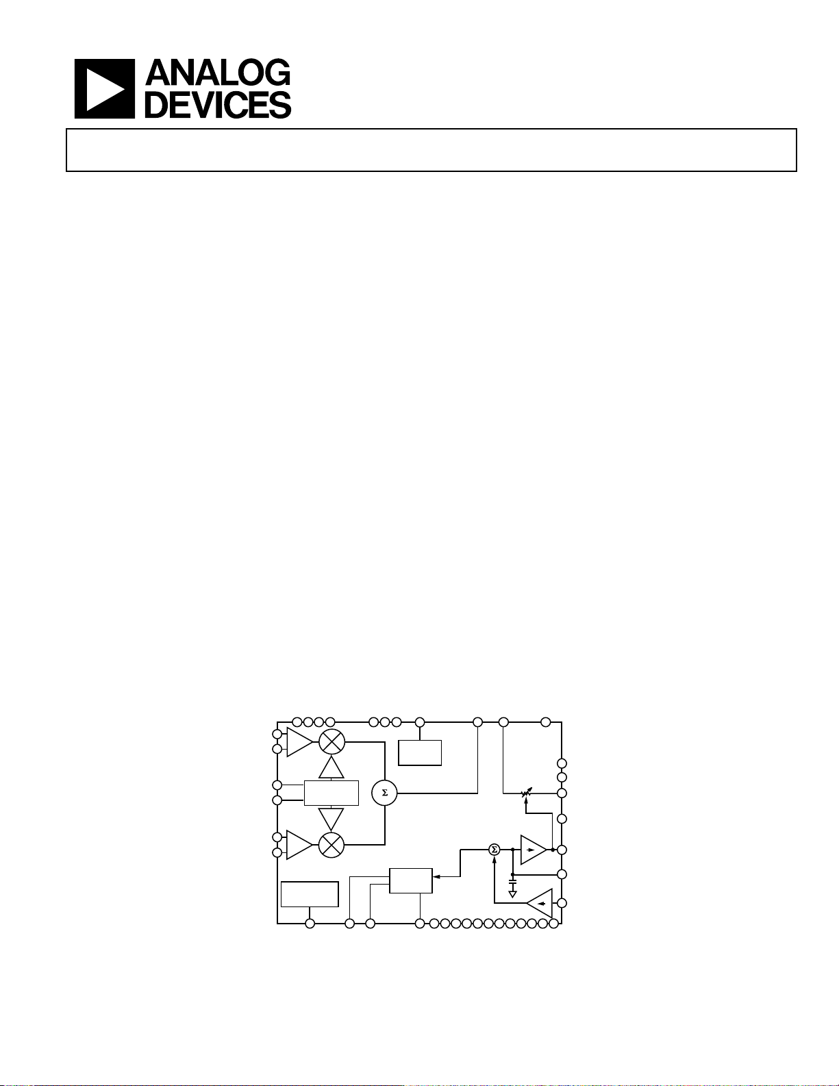
GENERAL DESCRIPTION
The ADL5386 is a quadrature modulator with unmatched
integration levels for low intermediate frequency (IF) and radio
frequency (RF) transmitters within broadband wireless access
systems, microwave radio links, cable modem termination
systems, and cellular infrastructure equipment. The ADL5386
operates over a frequency range of 50 MHz to 2200 MHz. Its
excellent phase accuracy and amplitude balance supports high data
rate, complex modulation for next-generation communication
infrastructure equipment.
with Integrated Detector and VVA
ADL5386
In addition, the ADL5386 incorporates a standalone
logarithmic power detector, as well as a voltage variable
attenuator (VVA). The attenuator has its own separate input and
output pins for easy cascading with filters and buffer amplifiers.
The wide dynamic range of the power detector and VVA provides
flexibility in the choice of the signal monitoring point in the
transmitter system.
The wide baseband input bandwidth of 700 MHz allows for
either baseband drive or a drive from a complex IF signal.
Typical applications are in IF or direct-to-RF radio-link
transmitters, cable modem termination systems, broadband
wireless access systems, and cellular infrastructure equipment.
The ADL5386 takes signals from two differential baseband inputs
and modulates them onto two carriers in quadrature with each
other. The two internal carriers are derived from a single-ended,
external local oscillator (LO) input signal at twice the frequency
as the desired output. The output amplifier is designed to drive
a 50 load.
The ADL5386 consists of two die, one fabricated using the
Analog Devices, Inc., advanced SiGe bipolar process, and the other
using an external GaAs process. The ADL5386 is packaged in a
40-lead, Pb-free LFCSP_VQ with an exposed paddle. Performance
is specified over the −40°C to +85°C range. A Pb-free evaluation
board is also available.
FUNCTIONAL BLOCK DIAGRAM
VPOS
25
IBBP
26
IBBN
33
LOIP
34
LOIN
29
QBBN
30
QBBP
TEMPERATURE
Rev. 0
Information furnished by Analog Devices is believed to be accurate and reliable. However, no
responsibility is assumed by Analog Devices for its use, nor for any infringements of patents or other
rights of third parties that may result from its use. Specifications subject to change without notice. No
license is granted by implication or otherwise under any patent or patent rights of Analog Devices.
Trademarks and registered trademarks are the property of their respective owners.
35 233638 37
QUADRATURE
PHASE
SPLITTER
SENSOR
8
TEMP INHIINLO
VPOS
12
22 21
DETECTOR
ENBL
24
IQ MOD
BIAS
LOG
39
Figure 1.
MODO UT
10
ADL5386
13511 161815 2819 27 3231 40
COMMTADJ
ATTI
NC
12
15dB
IV
9
ATTCM
17
14
ATTCM
20
ATTO
VREF
6
7
VDET/VCTL
4
CLPF
VSET
3
V
I
07664-001
One Technology Way, P.O. Box 9106, Norwood, MA 02062-9106, U.S.A.
Tel: 781.329.4700 www.analog.com
Fax: 781.461.3113 ©2009 Analog Devices, Inc. All rights reserved.
Page 2

ADL5386
TABLE OF CONTENTS
Features .............................................................................................. 1
Applications ....................................................................................... 1
General Description ......................................................................... 1
Functional Block Diagram .............................................................. 1
Revision History ............................................................................... 2
Specifications ..................................................................................... 3
Typical Input and Output Impedances ...................................... 8
Absolute Maximum Ratings ............................................................ 9
ESD Caution .................................................................................. 9
Pin Configuration and Function Descriptions ........................... 10
Typical Performance Characteristics ........................................... 12
Modulator .................................................................................... 12
Voltage Variable Attentuator ..................................................... 16
Detector ....................................................................................... 17
Closed-Loop AGC Mode........................................................... 18
Circuit Description ......................................................................... 19
Overview ...................................................................................... 19
Quadrature Modulator Section ................................................ 19
Logarithmic Detector ................................................................. 20
Voltage Variable Attenuator (VVA) ......................................... 20
Basic Connections .......................................................................... 21
Open-Loop Power Control Mode ............................................ 21
Power Supply and Grounding .................................................. 22
Device Enable and Disable ........................................................ 22
Baseband Inputs ......................................................................... 22
LO Input ...................................................................................... 22
AGC Mode .................................................................................. 22
Setting the TADJ Resistor .......................................................... 24
Using the Detector in Standalone Measurement Mode ........ 25
DAC Modulator Interfacing ..................................................... 25
Spectral Products from Harmonic Mixing ............................. 27
LO Generation Using PLLs ....................................................... 27
Transmit DAC Options ............................................................. 28
Modulator/Demodulator Options ........................................... 28
Evaluation Board ............................................................................ 29
Characterization Setup .................................................................. 31
SSB Setup ..................................................................................... 31
Detector Setup ............................................................................ 31
VVA S-Paramters Setup ............................................................. 32
VVA Intermodulation Test Setup ............................................. 32
Outline Dimensions ....................................................................... 33
Ordering Guide .......................................................................... 33
REVISION HISTORY
1/09—Revision 0: Initial Version
Rev. 0 | Page 2 of 36
Page 3

ADL5386
SPECIFICATIONS
Unless otherwise noted, VS = 5 V, TA = 25°C, LO = −7 dBm, I/Q inputs = 1.4 V p-p differential sine waves in quadrature on a 500 mV dc
bias, baseband frequency = 1 MHz, LO source and RF output load impedances are 50 Ω.
Table 1.
Parameter Conditions Min Typ Max Unit
MODULATOR DYNAMIC CHARACTERISTICS
Operating Frequency Range 50 2200 MHz
External LO Frequency Range External LO frequency is twice output frequency 100 4400 MHz
Output Frequency = 50 MHz
Output Power Single (lower) sideband output 5.6 dBm
Modulator Voltage Gain −1.3 dB
Output P1dB 10.8 dBm
Output Return Loss −21 dB
Carrier Leakage Unadjusted (nominal drive level) −43 dBm
At 85°C after optimization at 25°C −63 dBm
At −40°C after optimization at +25°C −63 dBm
Sideband Suppression Unadjusted (nominal drive level) −48 dBc
At 85°C after optimization at 25°C −60 dBc
At −40°C after optimization at +25°C −60 dBc
Quadrature Error −0.2 Degrees
I/Q Amplitude Balance 0.05 dB
Second Harmonic (fLO − (2 × fBB)), P
Third Harmonic (fLO + (3 × fBB)), P
Output IP2 F1 = 3.5 MHz, F2 = 4.5 MHz, P
Output IP3 F1 = 3.5 MHz, F2 = 4.5 MHz, P
Noise Floor 20 MHz offset from LO, all BB inputs at a bias of 500 mV −159 dBm/Hz
Output Frequency = 140 MHz
Output Power Single (lower) sideband output 5.7 dBm
Modulator Voltage Gain −1.2 dB
Output P1dB 11.1 dBm
Output Return Loss −21 dB
Carrier Leakage Unadjusted (nominal drive level) −42 dBm
At 85°C after optimization at 25°C −62 dBm
At −40°C after optimization at +25°C −62 dBm
Sideband Suppression Unadjusted (nominal drive level) −57 dBc
At 85°C after optimization at 25°C −60 dBc
At −40°C after optimization at +25°C −60 dBc
Quadrature Error −0.2 Degrees
I/Q Amplitude Balance 0.05 dB
Second Harmonic (fLO − (2 × fBB)), P
Third Harmonic (fLO + (3 × fBB)), P
Output IP2 F1 = 3.5 MHz, F2 = 4.5 MHz, P
Output IP3 F1 = 3.5 MHz, F2 = 4.5 MHz, P
Noise Floor 20 MHz offset from LO, all BB inputs at a bias of 500 mV −160 dBm/Hz
Output Frequency = 350 MHz
Output Power Single (lower) sideband output 4 5.5 7 dBm
Modulator Voltage Gain −1.4 dB
Output P1dB 11.1 dBm
Output Return Loss −19 dB
Carrier Leakage Unadjusted (nominal drive level) −38 dBm
At 85°C after optimization at 25°C −58 dBm
At −40°C after optimization at +25°C −58 dBm
= 5 dBm −80 dBc
OUT
= 5 dBm −58 dBc
OUT
= −3 dBm per tone 76 dBm
OUT
= −3 dBm per tone 26 dBm
OUT
= 5 dBm −79 dBc
OUT
= 5 dBm −56 dBc
OUT
= −3 dBm per tone 75 dBm
OUT
= −3 dBm per tone 25 dBm
OUT
Rev. 0 | Page 3 of 36
Page 4

ADL5386
Parameter Conditions Min Typ Max Unit
Sideband Suppression Unadjusted (nominal drive level) −46 dBc
At 85°C after optimization at 25°C −57 dBc
At −40°C after optimization at +25°C −57 dBc
Quadrature Error −0.5 Degrees
I/Q Amplitude Balance 0.05 dB
Second Harmonic (fLO − (2 × fBB)), P
Third Harmonic (fLO + (3 × fBB)), P
Output IP2 F1 = 3.5 MHz, F2 = 4.5 MHz, P
Output IP3 F1 = 3.5 MHz, F2 = 4.5 MHz, P
Noise Floor 20 MHz offset from LO, all BB inputs at a bias of 500 mV −160 dBm/Hz
20 MHz offset from LO, output power = −5 dBm −156 dBm/Hz
Output Frequency = 860 MHz
Output Power Single (lower) sideband output 3.8 5.3 6.8 dBm
Modulator Voltage Gain −1.6 dB
Output P1dB 11.4 dBm
Output Return Loss −15 dB
Carrier Leakage Unadjusted (nominal drive level) −37 dBm
At 85°C after optimization at 25°C −56 dBm
At −40°C after optimization at +25°C −56 dBm
Sideband Suppression Unadjusted (nominal drive level) −39 dBc
At 85°C after optimization at 25°C −55 dBc
At −40°C after optimization at +25°C −55 dBc
Quadrature Error −0.9 Degrees
I/Q Amplitude Balance 0.05 dB
Second Harmonic (fLO − (2 × fBB)), P
Third Harmonic (fLO + (3 × fBB)), P
Output IP2 F1 = 3.5 MHz, F2 = 4.5 MHz, P
Output IP3 F1 = 3.5 MHz, F2 = 4.5 MHz, P
Noise Floor 20 MHz offset from LO, all BB inputs at a bias of 500 mV −160 dBm/Hz
20 MHz offset from LO, output power = −5 dBm −157 dBm/Hz
Output Frequency = 1450 MHz
Output Power Single (lower) sideband output 4.3 dBm
Modulator Voltage Gain −2.6 dB
Output P1dB 10.6 dBm
Output Return Loss −15 dB
Carrier Leakage Unadjusted (nominal drive level) −35 dBm
At 85°C after optimization at 25°C −50 dBm
At −40°C after optimization at +25°C −50 dBm
Sideband Suppression Unadjusted (nominal drive level) −43 dBc
At 85°C after optimization at 25°C −45 dBc
At −40°C after optimization at +25°C −45 dBc
Quadrature Error −0.2 Degrees
I/Q Amplitude Balance 0.03 dB
Second Harmonic (fLO − (2 × fBB)), P
Third Harmonic (fLO + (3 × fBB)), P
Output IP2 F1 = 3.5 MHz, F2 = 4.5 MHz, P
Output IP3 F1 = 3.5 MHz, F2 = 4.5 MHz, P
Noise Floor 20 MHz offset from LO, all BB inputs at a bias of 500 mV −160 dBm/Hz
= 5 dBm −76 dBc
OUT
= 5 dBm −53 dBc
OUT
= −3 dBm per tone 74 dBm
OUT
= −3 dBm per tone 25 dBm
OUT
= 5 dBm −72 dBc
OUT
= 5 dBm −49 dBc
OUT
= −3 dBm per tone 73 dBm
OUT
= −3 dBm per tone 25 dBm
OUT
= 5 dBm −67 dBc
OUT
= 5 dBm −45 dBc
OUT
= −3 dBm per tone 63 dBm
OUT
= −3 dBm per tone 25 dBm
OUT
Rev. 0 | Page 4 of 36
Page 5

ADL5386
Parameter Conditions Min Typ Max Unit
Output Frequency = 1900 MHz
Output Power Single (lower) sideband output 3.2 dBm
Modulator Voltage Gain −3.7 dB
Output P1dB 9.2 dBm
Output Return Loss −13 dBm
Carrier Leakage Unadjusted (nominal drive level) −35 dBm
At 85°C after optimization at 25°C −53 dBm
At −40°C after optimization at +25°C −53 dBm
Sideband Suppression Unadjusted (nominal drive level) −30 dBc
At 85°C after optimization at 25°C −45 dBc
At −40°C after optimization at +25°C −45 dBc
Quadrature Error −3 Degrees
I/Q Amplitude Balance 0.02 dB
Second Harmonic (fLO − (2 × fBB)), P
Third Harmonic (fLO + (3 × fBB)), P
Output IP2 F1 = 3.5 MHz, F2 = 4.5 MHz, P
Output IP3 F1 = 3.5 MHz, F2 = 4.5 MHz, P
Noise Floor 20 MHz offset from LO, all BB inputs at a bias of 500 mV −160 dBm/Hz
20 MHz offset from LO, output power = −5 dBm −156 dBm/Hz
Output Frequency = 2150 MHz
Output Power Single (lower) sideband output 2.5 dBm
Modulator Voltage Gain −4.4 dB
Output P1dB 8.4 dBm
Output Return Loss −11 dB
Carrier Leakage Unadjusted (nominal drive level) −35 dBm
At 85°C after optimization at 25°C −48 dBm
At −40°C after optimization at +25°C −46 dBm
Sideband Suppression Unadjusted (nominal drive level) −34 dBc
At 85°C after optimization at 25°C −45 dBc
At −40°C after optimization at +25°C −45 dBc
Quadrature Error −1.2 Degrees
I/Q Amplitude Balance 0.03 dB
Second Harmonic (fLO − (2 × fBB)), P
Third Harmonic (fLO + (3 × fBB)), P
Output IP2 F1 = 3.5 MHz, F2 = 4.5 MHz, P
Output IP3 F1 = 3.5 MHz, F2 = 4.5 MHz, P
Noise Floor 20 MHz offset from LO, all BB inputs at a bias of 500 mV −160 dBm/Hz
20 MHz offset from LO, output power = −5 dBm −155 dBm/Hz
LO Inputs Pin LOIP and Pin LOIN
LO Drive Level Characterization performed at typical level −13 −7 +2 dBm
Characterization performed at typical level (<140 MHz) −7 −7 +2 dBm
Input Impedance 50 Ω
Input Return Loss 350 MHz, LOIN ac-coupled to ground −7 dB
Baseband Inputs Pin IBBP, Pin IBBN, Pin QBBP, Pin QBBN
I and Q Input Bias Level 500 mV
Input Bias Current −60 μA
Bandwidth (0.1 dB) fLO = 2 × 900 MHz, P
Bandwidth (3 dB) fLO = 2 × 900 MHz, P
= 5 dBm −59 dBc
OUT
= 5 dBm −45 dBc
OUT
= −3 dBm per tone 55 dBm
OUT
= −3 dBm per tone 23 dBm
OUT
= 5 dBm −56 dBc
OUT
= 5 dBm −48 dBc
OUT
= −3 dBm per tone 53 dBm
OUT
= −3 dBm per tone 21 dBm
OUT
≈ −4 dBm 50 MHz
OUT
≈ −4 dBm 700 MHz
OUT
Rev. 0 | Page 5 of 36
Page 6

ADL5386
Parameter Conditions Min Typ Max Unit
VOLTAGE VARIABLE AT TENUATOR
Pin VCTL, Pin ATTI, and Pin ATTO, open-loop mode,
attenuation control applied to VCTL
Output Frequency = 50 MHz
Insertion Loss Minimum attenuation, V
Attenuation Range Attenuation at V
= 2 V − Attenuation at V
VCTL
= 2 V 1.7 dB
VCTL
= 0 V 37.8 dB
VCTL
Return Loss 17 dB
Input IP3
Minimum attenuation, V
= 2 V, Δf = 1 MHz,
VCTL
input power = −3 dBm per tone
Output Frequency = 140 MHz
Insertion Loss Minimum attenuation, V
Attenuation Range Attenuation at V
= 2 V − Attenuation at V
VCTL
= 2 V 1.9 dB
VCTL
= 0 V 37 dB
VCTL
Return Loss 17 dB
Input IP3
Minimum attenuation, V
= 2 V, Δf = 1 MHz,
VCTL
input power = −3 dBm per tone
Output Frequency = 350 MHz
Insertion Loss Minimum attenuation, V
Attenuation Range Attenuation at V
= 2 V − Attenuation at V
VCTL
= 2 V 2.2 dB
VCTL
= 0 V 26.2 dB
VCTL
Return Loss 17 dB
Input IP3
Minimum attenuation, V
= 2 V, Δf = 1 MHz,
VCTL
input power = −3 dBm per tone
Output Frequency = 860 MHz
Insertion Loss Minimum attenuation, V
Attenuation Range Attenuation at V
= 2 V − Attenuation at V
VCTL
= 2 V 2.5 dB
VCTL
= 0 V 21 dB
VCTL
Return Loss 14 dB
Input IP3
Minimum attenuation, V
= 2 V, Δf = 1 MHz,
VCTL
input power = −3 dBm per tone
Output Frequency = 1900 MHz
Insertion Loss Minimum attenuation, V
Attenuation Range Attenuation at V
= 2 V − Attenuation at V
VCTL
= 2 V 3 dB
VCTL
= 0 V 19 dB
VCTL
Return Loss 13 dB
Input IP3
Minimum attenuation, V
= 2 V, Δf = 1 MHz,
VCTL
input power = −3 dBm per tone
Output Frequency = 2150 MHz
Insertion Loss Minimum attenuation, V
Attenuation Range Attenuation at V
= 2 V − Attenuation at V
VCTL
= 2 V 3.3 dB
VCTL
= 0 V 17 dB
VCTL
Return Loss 13 dB
Input IP3
Minimum attenuation, V
= 2 V, Δf = 1 MHz,
VCTL
input power = −3 dBm per tone
SWITCHING CHARACTERISTICS ATTCM (Pin 14 and Pin 17) = 1000 pF
VCTL Response Time
LOG DETECTOR
Frequency = 350 MHz, V
50 % of V
to10% of RF envelope
VCTL
Frequency = 350 MHz, V
50 % of V
to 90% of RF envelope
VCTL
In measurement mode, VDET/VCTL is shorted to VSET;
= 2 V to 0 V; measured from
VCTL
= 0 V to 2 V; measured from
VCTL
in controller mode, the setpoint voltage is applied to VSET;
the CW input signal is applied at INHI
f = 50 MHz R
= 22.1 kΩ
TAD J
±1 dB Dynamic Range TA = 25°C 28 dB
Slope1 −21 mV/dB
Intercept1 18.2 dBm
VDET or VSET Voltage PIN = −10 dBm 0.59 V
PIN = −30 dBm 1.01 V
36 dBm
36 dBm
35 dBm
35 dBm
36 dBm
35 dBm
125 ns
15 ns
Rev. 0 | Page 6 of 36
Page 7

ADL5386
Parameter Conditions Min Typ Max Unit
f = 140 GHz R
±1 dB Dynamic Range TA = 25°C 28 dB
Slope1 −21.1 mV/dB
Intercept1 17.8 dBm
VDET or VSET Voltage PIN = −10 dBm 0.59 V
PIN = −30 dBm 1.01 V
f = 350 MHz R
±1 dB Dynamic Range TA = 25°C 26 dB
Slope1 −21.3 mV/dB
Intercept1 17.1 dBm
VDET or VSET Voltage PIN = −10 dBm 0.58 V
PIN = −30 dBm 1.0 V
f = 860 MHz R
±1 dB Dynamic Range TA = 25°C 25 dB
Slope1 −21.6 mV/dB
Intercept1 16.2 dBm
VDET or VSET Voltage PIN = −10 dBm 0.57 V
PIN = −30 dBm 1.00 V
f = 1900 MHz R
±1 dB Dynamic Range TA = 25°C 26 dB
Slope1 −22.7 mV/dB
Intercept1 13.5 dBm
VDET or VSET Voltage PIN = −10 dBm 0.54 V
PIN = −30 dBm 0.99 V
f = 2150 MHz R
±1 dB Dynamic Range TA = 25°C 24 dB
Slope1 −23.2 mV/dB
Intercept1 12.6 dBm
VDET or VSET Voltage PIN = −10 dBm 0.53 V
PIN = −30 dBm 0.99 V
LOG DETECTOR OUTPUT INTERFACE VDET
VDET Voltage Swing V
V
Small Signal Bandwidth Simulated, INHI = −10 dBm, from CLPF to VOUT >100 MHz
Output Noise INHI = 2.2 GHz, –10 dBm, f
Fall Time Input level = no signal to −10 dBm, 90% to 10%, C
Input level = no signal to −10 dBm, 90% to 10%, C
Rise Time Input level = −10 dBm to no signal, 10% to 90%, C
Input level = −10 dBm to no signal, 10% to 90%, C
Video Bandwidth 15 MHz
VSET Incremental Input Resistance P
VSET Input Bias Current P
TAD J INTERFACE TADJ
Input Resistance TADJ = 0.9 V, sourcing 50 μA 13 kΩ
Disable Threshold Voltage TADJ = open V
TEMPERATURE SENSOR OUTPUT TEMP
Output Voltage TA = 27.15°C, 300K, RL = 1 MΩ (after full warmup) 1.45 V
Temperature Slope −40°C ≤ TA ≤ +85°C, RL = 1 MΩ 4.6 mV/°C
Output Impedance 1 kΩ
= 22.1 kΩ
TAD J
= 22.1 kΩ
TAD J
= 22.1 kΩ
TAD J
= 22.1 kΩ
TAD J
= 22.1 kΩ
TAD J
= 0 V, INHI = open, controller mode 2 V
VSET
= 2 V, INHI = open, controller mode 10 mV
VSET
= 0 dBm, AGC mode, V
OUT
= 0 dBm, AGC mode, V
OUT
= 100 kHz, C
NOISE
= 0.9 V to 1 V 33,000 dV/dI
VSET
= 1 V 25 μA
VSET
= open 73 nV/√Hz
CLPF
= 8 pF 42 ns
CLPF
= 0.1 μF 178 μs
CLPF
= 8 pF 29 ns
CLPF
= 0.1 μF 174 μs
CLPF
− 0.4 V
VPOS
Rev. 0 | Page 7 of 36
Page 8

ADL5386
Parameter Conditions Min Typ Max Unit
ENABLE INPUT ENBL
Input Bias Current ENBL = 5 V 0.5 μA
ENBL = 0 V −0.7 μA
ENBL High Level (Logic 1) 1.5 V
ENBL Low Level (Logic 0) 0.4 V
POWER SUPPLIES Pin VPOS
Voltage 4.75 5.5 V
Supply Current ENBL = high 230 245 mA
In sleep mode, ENBL = low and TADJ = high 2.2 mA
In detector disabled mode, ENBL = high and TADJ = high 215 mA
1
Slope and intercept are determined by calculating the best-fit line between the power levels of −33 dBm and −10 dBm at the specified input frequency.
TYPICAL INPUT AND OUTPUT IMPEDANCES
Unless otherwise noted, VS = 5 V, TA = 25°C. All impedances are normalized to 50 Ω. The effects of the test fixture are de-embedded up to
the pins of the device.
Table 2.
Frequency (MHz) LO Input Impedance at 2× Frequency Modulator Output Impedance Detector Input Impedance
50 1.393 − j0.027 0.847 − j0.016 28.463 − j11.386
140 1.406 + j0.013 0.839 + j0.019 15.159 − j15.234
350 1.441 + j0.039 0.82 + j0.065 4.661 − j10.6
860 1.66 + j0.077 0.764 + j0.166 1.158 − j4.58
1450 2.261 − j0.304 0.799 + j0.231 0.567 − j2.545
1900 1.436 − j1.898 0.856 + j0.371 0.375 − j1.866
2150 0.517 − j1.446 0.862 + j0.51 0.308 − j1.652
Rev. 0 | Page 8 of 36
Page 9
ADL5386
ABSOLUTE MAXIMUM RATINGS
Table 3.
Parameter Rating
Supply Voltage, VPOS 5.5 V
IBBP, IBBN, QBBP, QBBN Range 0 V to 2.0 V
LOIP and LOIN 13 dBm
Internal Power Dissipation 1.4 W
θJA (Exposed Paddle Soldered Down) 38°C/W
Maximum Junction Temperature 150°C
Operating Temperature Range −40°C to +85°C
Storage Temperature Range −65°C to +150°C
Stresses above those listed under Absolute Maximum Ratings
may cause permanent damage to the device. This is a stress
rating only; functional operation of the device at these or any
other conditions above those indicated in the operational
section of this specification is not implied. Exposure to absolute
maximum rating conditions for extended periods may affect
device reliability.
ESD CAUTION
Rev. 0 | Page 9 of 36
Page 10

ADL5386
A
V
V
PIN CONFIGURATION AND FUNCTION DESCRIPTIONS
TTIMO DOUT
12
10
15dB
IV
9
ATTCM
17
14
ATTCM
20
ATTO
6
VREF
7
VDET/VCTL
4
CLPF
VSET
3
V
I
IBBP
IBBN
LOIP
LOIN
QBBN
QBBP
25
26
33
34
29
30
TEMPERATURE
SENSOR
POS
35 233638 37
QUADRATURE
PHASE
SPLITTER
ENBL NC
POS
22
21
24
IQ MOD
BIAS
ADL5386
LOG
DETECTOR
8
TEMP I NHIINLO
NOTES
1. NC = NO CONNEC T.
2. CONNECT T HE EXPOSED PAD TO GROUND VIA A LOW IMPEDANCE PATH.
12
39
13511 161815 2819 27 3231 40
COMMTADJ
07664-002
Figure 2. Pin Configuration
Table 4. Pin Function Descriptions
Pin No. Mnemonic Description
1 INLO Detector Common. This pin should be ac-coupled to ground.
2 INHI
Detector Input. When operating in AGC mode, a portion of the signal at the output of the VVA (or at the
output of a subsequent stage) is coupled back to this input. The signal should be ac-coupled into INHI. To provide
a 50 Ω match at INHI, a 50 Ω resistor should be connected between INHI and ground (with the ac-coupling
capacitor placed between the resistor and the INHI pin).
3 VSET Setpoint Input. Setpoint input for controller mode or feedback input for measurement mode.
4 CLPF
AGC Loop Filter Capacitor. The ground-referenced capacitor that is connected to this pin sets the loop bandwidth
of the AGC circuit.
5, 11, 13, 15,
COMM Device Common. Connect these pins to the same low impedance ground plane.
16, 18, 19, 27,
28, 31, 32, 40
6 VREF
Attenuator Control Voltage Reference. In AGC mode, this pin should be left open. In open-loop mode, when
the VVA is being controlled externally, a 2 V reference voltage should be applied to this pin.
7 VDET/VCTL
Detector Output/VVA Control Voltage Input. When the VVA is being controlled externally (open-loop mode),
the attenuation is controlled by the external voltage applied to this pin. The VVA control range is from 0 V
(maximum attenuation) to 2 V (minimum attenuation). In this mode, VREF (Pin 6) should be tied to approximately
2 V. When the VVA is being operated in AGC mode, this pin is left open with the voltage on the pin representing the
AGC drive voltage to the VVA. If the VVA is not being used, the AGC log amp can be used as a standalone detector
by connecting this pin to VSET. In this mode, the log amp output voltage is available at this pin.
8 TEMP
Temperature Sensor Output. This pin provides a standalone temperature sensor output voltage. At room
temperature, the nominal output voltage is equal to 1.45 V. The slope of the output voltage is equal to 4.6 mV/°C.
9 NC No Connect. Do not connect this pin.
10 MODOUT
RF Output of IQ Modulator. Single-ended, 50 Ω internally biased RF output. MODOUT is generally
ac-coupled to the input of the VVA (either ATTI or ATTO).
12, 20 ATTI, ATTO
VVA RF Input/Output. ATTI is normally ac-coupled to MODOUT. However, because the VVA is completely reversible,
MODOUT can also drive ATTO with ATTI operating as the VVA output.
14, 17 ATTCM VVA Input/Output Common. These pins should be ac-coupled to ground.
21 to 23,
35 to 38
VPOS
Power Supply. Positive supply voltage pins. All pins should be connected to the same supply (VS). To ensure
adequate external bypassing, connect a 0.1 μF capacitor between each pin and ground.
Rev. 0 | Page 10 of 36
Page 11

ADL5386
Pin No. Mnemonic Description
24 ENBL
25, 26, 29, 30
33 LOIP
34 LOIN Local Oscillator Common. This pin should be ac-coupled to ground.
39 TADJ
41 (EPAD)
IBBP, IBBN,
QBBN, QBBP
Exposed
Pad (EPAD)
IQ Modulator Enable. The IQ modulator is enabled by connecting this pin to VPOS and is disabled by connecting
ENBL to ground.
Differential In-Phase and Quadrature Baseband Inputs. These high impedance inputs should be dc-biased to 0.5 V.
Nominal characterized ac signal swing is 700 mV p-p on each pin, resulting in a differential drive of
1.4 V p-p on each input pair. These inputs are not self-biased and have to be externally biased.
Local Oscillator Input. The local oscillator signal, at two times the output frequency, should be ac-coupled into
this pin.
Temperature Compensation Adjustment Pin and Detector Enable/Disable. This pin is primarily used to
provide temperature compensation to the on-chip log amp based AGC circuit. The correct compensation
current is set by connecting a ground-referenced resistor to this pin. A value of 22.1 kΩ is recommended
for the frequencies over which the ADL5386 is specified. The TADJ pin can also be used to power down the
detector section of the ADL5386 by connecting it to VPOS. The detector must be disabled when the
modulator/VVA is operating in open loop mode.
Connect the exposed pad to ground via a low impedance path.
Rev. 0 | Page 11 of 36
Page 12

ADL5386
TYPICAL PERFORMANCE CHARACTERISTICS
MODULATOR
Unless otherwise noted, VS = 5 V, TA = 25°C, LO = −7 dBm, I/Q inputs = 1.4 V p-p differential sine waves in quadrature on a 500 mV dc bias, baseband
frequency = 1 MHz, LO source and RF output load impedances are 50 Ω.
14
13
12
11
10
SSB OUTPUT POWER, OUTPUT P1dB (d Bm)
Figure 3. Single Sideband (SSB) Output Power (P
OUTPUT P1dB
9
8
SSB OUTPUT P OWER
7
6
5
4
3
2
1
50 550 1050 1550 2050
OUTPUT FREQUENCY (MHz)
VS = 5.5V
= 5.0V
V
S
= 4.75V
V
S
), Output P1dB vs.
OUT
07664-003
Output Frequency and Power Supply
14
13
12
11
10
SSB OUTPUT POWER, OUTPUT P1dB (dBm)
Figure 4. Single Sideband (SSB) Output Power (P
OUTPUT P1dB
9
8
SSB OUTPUT P OWER
7
6
5
4
3
2
1
50 550 1050 1550 2050
OUTPUT FREQUENCY (MHz)
OUT
+85°C
+25°C
–40°C
), Output P 1 dB vs.
07664-004
Output Frequency and Temperature
–20
–30
CARRIER FEEDTHRO UGH
–40
SIDEBAND SUPPRESSI ON
–50
–60
–70
SECOND-ORDER DIS TORTIO N (dBc),
THIRD-ORDER DIS TORTIO N (dBc), CARRIER
–80
0.1
FEEDTHROUGH ( dBm), SIDEBAND SUP PRESSION (d Bc)
SSB OUTPUT PO WER
THIRD-ORDER
DISTORTI ON
SECOND-ORDER
DISTORTION
DIFFERENTI AL BASEBAND VOLT AGE (V p-p )
1.0
15
10
5
0
–5
SSB OUTPUT PO WER (dBm)
–10
–15
10
Figure 5. Second- and Third-Order Distortion, Carrier Feedthrough, Sideband
Suppression, and SSB Output Power vs. Differential Baseband Voltage,
Output Frequency = 350 MHz
Rev. 0 | Page 12 of 36
07664-005
–20
SSB OUTPUT POWER
–30
CARRIER FEEDTHROUGH
–40
SIDEBAND SUP PRESSIO N
–50
–60
–70
SECOND-OR DER DISTO RTION ( dBc),
THIRD-ORD ER DISTO RTION ( dBc), CARRIE R
FEEDTHRO UGH (dBm) , SIDEBAND SUPPRESSI ON (dBc)
–80
0.1
DIFFERE NTIAL BAS EBAND VOLT AGE (V p-p)
1.0
THIRD-O RDER
DISTORTION
SECOND-O RDER
DISTORTION
15
10
5
0
–5
–10
–15
10
Figure 6. Second- and Third-Order Distortion, Carrier Feedthrough, Sideband
Suppression, and SSB Output Power vs. Differential Baseband Voltage,
Output Frequency = 860 MHz
90
80
70
60
50
40
30
OUTPUT IP2 AND IP3 (dBm)
20
10
0
50 550 1050 1550 2050
OUTPUT FREQUENCY (MHz)
OIP2
OIP3
+85°C
+25°C
–40°C
07664-007
Figure 7. Output IP2 and IP3 vs. Output Frequency and Temperature
2
1
0
–1
–2
–3
–4
–5
–6
–7
–8
BASEBAND FREQUENCY RESP ONSE (dB)
–9
–10
1 10 100 1000
BB FREQUENCY (MHz)
07664-008
Figure 8. Baseband Frequency Response Normalized to Response for 1 MHz
BB Signal, Carrier Frequency = 500 MHz
SSB OUTPUT POWE R (dBm)
07664-006
Page 13

ADL5386
–
20
–30
–40
–50
–60
CARRIER FEEDTHROUGH (dBm)
–70
–80
50 550 1050 1550 2050
OUTPUT FREQUENCY (MHz)
+85°C
+25°C
–40°C
Figure 9. Carrier Feedthrough Distribution vs. Output Frequency and
Temperature
0
–10
–20
–30
–40
–50
–60
–70
CARFRIER FEEDT HROUGH (dBm)
–80
–90
50 550 1050 1550 2050
OUTPUT FREQUENCY (MHz)
+85°C
+25°C
–40°C
Figure 10. Carrier Feedthrough Distribution at Temperature Extremes,
After Nulling to < −65 dBm at T
0.010
0.008
0.006
0.004
0.002
0
–0.002
OFFSET (V)
–0.004
–0.006
–0.008
–0.010
50 550 1050 1550 2050
I OFFSET
Q OFFSET
OUTPUT F REQUENCY (MHz)
= 25°C vs. Output Frequency
A
Figure 11. Distribution of I Offset and Q Offset Required to Null Carrier
Feedthrough vs. Output Frequency
0
–10
–20
–30
–40
–50
–60
–70
SIDEBAND SUPPRESSIO N (dBc)
–80
07664-009
–90
50 550 1050 1550 2050
OUTPUT FREQUENCY (MHz)
+85°C
+25°C
–40°C
07664-012
Figure 12. Sideband Suppression vs. Output Frequency and Temperature
0
–10
–20
–30
–40
–50
–60
–70
SIDEBAND SUPPRESSION (dBc)
–80
07664-010
–90
50 550 1050 1550 2050
OUTPUT FREQUENCY (MHz)
+85°C
+25°C
–40°C
07664-013
Figure 13. Sideband Suppression Distribution at Temperature Extremes,
After Sideband Suppression Nulled to < −50 dBc at T
= 25°C vs.
A
Output Frequency
0.20
0.15
0.10
0.05
0
–0.05
–0.10
IQ AMPLI TUDE OFF SET (dB)
–0.15
–0.20
07664-011
50 550 1050 1550 2050
OUTPUT FREQUENCY (MHz)
PEAK IQ AMPLITUDE OFFSET
IQ PHASE
94
93
92
91
90
89
IQ PHASE (Degrees)
88
87
86
07664-014
Figure 14. Distribution of Peak Q Amplitude to Null Undesired Sideband
(Peak I Amplitude Held Constant at 0.7 V) and Distribution of IQ Phase to
Null Undesired Sideband vs. Output Frequency
Rev. 0 | Page 13 of 36
Page 14

ADL5386
–
–
–
20
–30
–40
–50
–60
–70
CARRIER FEEDTHRO UGH (dBm)
–80
–90
–7 –6
–5 –4 –2 –1–3 012
LO AMPLI TUDE (dBm)
Figure 15. Carrier Feedthrough Distribution vs. LO Amplitude
at 50 MHz and 350 MHz
20
–30
–40
50MHz
350MHz
50MHz
350MHz
j1
j0.5
2250MHz
100MHz
50MHz
S11 OF LOIP
S22 OF MO D OUTPUT
S11 OF DETECTOR INPUT
4500MHz
07664-015
–j0.5
2250MHz
–j1
j2
–j2
50MHz
07664-018
Figure 18. Modulator Output Impedance, LO Input Impedance and Detector
Input Impedance (Unterminated) vs. Frequency
0
–5
–50
–60
–70
SIDEBAND SUPPRESSION (dBc)
–80
–90
–7 –6
–5 –4 –2 –1–3 012
LO AMPLI TUDE (dBm)
Figure 16. Sideband Suppression Distribution vs. LO Amplitude
at 50 MHz and 350 MHz
20
–30
–40
–50
–60
SIDEBAND SUPPRESSION (dBc)
–70
1
BASEBAND FREQUENCY (M Hz)
10
Figure 17. Sideband Suppression vs. Baseband Frequency,
Output Frequency = 350 MHz
100
–10
RETURN LOSS (dB)
–15
07664-016
–20
0.5 1.0 1.5 2. 0 2.5
LOIP FREQUENCY (GHz )
3.0 3.5 4.004.5
07664-019
Figure 19. LO Port Input Return Loss vs. LOIP Frequency
30
25
20
15
10
NUMBER OF PARTS
5
07664-017
0
–157.6
–158.2
–158.0
OFFSET FROM O UTPUT FREQUENCY (dBm/Hz at 20MHz)
–157.4
–157.8
–157.2
–157.0
–156.8
–156.6
–156.4
07664-020
–156.2
–156.0
Figu re 20. 20 MH z Offs et Noise Floor Distribution, Output Frequency = 360 MHz,
= −5 dBm, QPSK Carrier, Symbol Rate = 3. 84 MSPS
P
OUT
Rev. 0 | Page 14 of 36
Page 15

ADL5386
35
30
25
20
15
NUMBER OF PARTS
10
250
225
200
175
150
VS= 5.5V
V
= 5.0V
S
V
= 4.75V
S
POWER SUPPL Y CURRENT
WITH MODULATOR ENABLE D
AND DETECTOR DIS ABLED
POWER SUPPL Y CURRENT
WITH MODUL ATOR DISABLE D
AND DETECTOR ENABL ED
26
24
22
20
18
5
0
–155.8
–156.0
OFFSET FROM O UTPUT FREQUENCY (dBm/Hz at 20MHz)
–155.4
–155.6
–155.2
–154.8
–155.0
–154.6
–154.4
07664-021
–154.2
–154.0
Figure 21. 20 MHz Offset Noise Floor Distribution, Output Frequency =
860 MHz, P
= −5 dBm, 64 QAM Carrier, Symbol Rate = 5 MSPS
OUT
125
100
MODULATOR S UPPLY CURRENT (mA)
75
–40
25
TEMPERATURE (° C)
85
16
14
12
Figure 22. Power Supply Current vs. Temperature and Supply Voltage
DETECTOR SUPPLY CURRENT (mA)
07664-022
Rev. 0 | Page 15 of 36
Page 16

ADL5386
m
m
m
d
m
d
m
d
m
VOLTAGE VARIABLE ATTENTUATOR
Unless otherwise noted, VS = 5 V, TA = 25°C.
80
70
+85°C
60
)
INPUT IP3 AND INPUT IP2 (dB
–10
–20
–30
–40
–50
–60
+25°C
50
–40°C
40
30
20
10
ATTENUATIO N
0
0 0.2 0.4 0.6 0.8 1.0 1.2 1.4 1.6 1.8 2.0
INPUT IP2
V
(V)
VCTL
INPUT IP3
RETURN LOSS
Figure 23. IIP3, IIP2, Attenuation, and Return Loss vs.
Voltage and Temperature at 140 MHz
V
VCTL
80
+85°C
70
+25°C
60
)
INPUT IP3 AND INPUT IP2 (dB
–10
–20
–30
–40
–50
–60
–40°C
50
40
30
20
10
ATTENUATION
0
0 0.2 0.4 0.6 0.8 1.0 1.2 1.4 1.6 1.8 2.0
V
VCTL
INPUT IP2
RETURN LOSS
(V)
Figure 24. IIP3, IIP2, Attenuation, and Return Loss vs.
Voltage and Temperature at 350 MHz
V
VCTL
80
+85°C
70
+25°C
60
)
INPUT IP3 AND INPUT IP2 (dB
–10
–20
–30
–40
–50
–60
–40°C
50
40
30
20
10
0
0 0.2 0.4 0.6 0.8 1.0 1.2 1.4 1.6 1.8 2.0
INPUT IP2
INPUT IP3
ATTENUATION
V
VCTL
RETURN LOSS
(V)
INPUT IP3
25
20
15
10
5
0
–5
–10
–15
–20
–25
–30
–35
–40
–45
25
20
15
10
5
0
–5
–10
–15
–20
–25
–30
–35
–40
–45
25
20
15
10
5
0
–5
–10
–15
–20
–25
–30
–35
–40
–45
80
+85°C
70
+25°C
–40°C
60
)
50
B
40
30
20
10
0
–10
–20
–30
INPUT IP3 AN D INPUT IP2 (
ATTENUATION AND RETURN LOSS (dB)
07664-023
–40
–50
–60
0 0.2 0.4 0.6 0.8 1.0 1.2 1.4 1.6 1.8 2.0
INPUT IP2
INPUT IP3
ATTENUATI ON
RETURN LOSS
V
(V)
VCTL
Figure 26. IIP3, IIP2, Attenuation, and Return Loss vs.
Voltage and Temperature at 1450 MHz
V
VCTL
80
70
60
)
50
B
40
30
20
10
0
–10
–20
+85°C
–30
INPUT IP3 AND INPUT IP2 (
ATTENUATION AND RETURN L OSS (dB)
07664-024
+25°C
–40
–40°C
–50
–60
0 0.2 0.4 0.6 0.8 1.0 1.2 1.4 1.6 1.8 2.0
INPUT IP2
INPUT IP3
ATTENUATI ON
RETURN LOSS
V
(V)
VCTL
Figure 27. IIP3, IIP2, Attenuation, and Return Loss vs.
V
Voltage and Temperature at 1900 MHz
VCTL
80
70
60
)
50
B
40
30
20
10
0
–10
–20
–30
INPUT IP3 AN D INPUT IP2 (
+85°C
–40
ATTENUATION AND RETURN L OSS (dB)
07664-025
+25°C
–50
–40°C
–60
0 0.2 0.4 0.6 0.8 1.0 1.2 1.4 1.6 1.8 2.0
INPUT IP2
INPUT IP3
ATTENUATI ON
V
(V)
VCTL
RETURN LOSS
25
20
15
10
5
0
–5
–10
–15
–20
–25
–30
–35
–40
–45
25
20
15
10
5
0
–5
–10
–15
–20
–25
–30
–35
–40
–45
25
20
15
10
5
0
–5
–10
–15
–20
–25
–30
–35
–40
–45
ATTENUATION AND RETURN L OSS (dB)
07664-026
ATTENUATION AND RETURN LOSS (dB)
07664-027
ATTENUATION AND RETURN L OSS (dB)
07664-028
Figure 25. IIP3, IIP2, Attenuation, and Return Loss vs.
Voltage and Temperature at 860 MHz
V
VCTL
Figure 28. IIP3, IIP2, Attenuation, and Return Loss vs.
V
Voltage and Temperature at 2150 MHz
VCTL
Rev. 0 | Page 16 of 36
Page 17

ADL5386
V
V
DETECTOR
Unless otherwise noted, VS = 5 V, TA = 25°C.
1.50
1.25
+85°C
+25°C
–40°C
3
2
1.50
1.25
+85°C
+25°C
–40°C
3
2
1.00
(V)
VSET
0.75
/
VDET
V
0.50
0.25
0
–45 –25–35 –15 –5 5
Figure 29. V
1.50
1.25
1.00
(V)
VSET
0.75
/
VDET
V
0.50
0.25
0
–45 –25–35 –15 –5 5
Figure 30. V
Voltage and Log Conformance vs. Input Amplitude at
VDET/VVSET
Voltage and Log Conformance vs. Input Amplitude at
VDET/VVSET
350 MHz, R
+85°C
+25°C
–40°C
860 MHz, R
PIN (dBm)
= 22.1 kΩ
TADJ
PIN (dBm)
= 22.1 kΩ
TADJ
1
0
–1
POWER ERROR ( dB)
–2
07664-029
–3
3
2
1
0
–1
POWER ERROR ( dB)
–2
07664-030
–3
1.00
(V)
VSET
0.75
/V
VDET
V
0.50
0.25
0
–45 –25–35 –15 –5 5
Figure 31. V
VDET/VVSET
Amplitude at 1450 MHz, R
1.50
1.25
1.00
(V)
VSET
0.75
/V
VDET
V
0.50
0.25
0
–45 –25–35 –15 –5 5
Figure 32. V
VDET/VVSET
Amplitude at 2150 MHz, R
PIN (dBm)
Voltage and Log Conformance vs. Input
= 22.1 kΩ
TADJ
+85°C
+25°C
–40°C
PIN (dBm)
Voltage and Log Conformance vs. Input
= 22.1 kΩ
TADJ
1
0
–1
POWER ERROR (dB)
–2
07664-031
–3
3
2
1
0
–1
POWER ERROR ( dB)
–2
07664-032
–3
Rev. 0 | Page 17 of 36
Page 18

ADL5386
CLOSED-LOOP AGC MODE
Unless otherwise noted, VS = 5 V, TA = 25°C, LO = −7 dBm, I/Q inputs = 1.4 V p-p differential sine waves in quadrature on a 500 mV dc bias,
baseband frequency = 1 MHz, LO source and RF output load impedances are 50 Ω. For AGC mode characterization setup, refer to Figure 42.
5
0
+85°C
–
5
+25°C
–40°C
–10
(dBm)
–15
OUT
P
–20
4
3
2
1
0
ERROR (dB)
–1
5
0
–
5
–10
(dBm)
–15
OUT
P
–20
+85°C
+25°C
–40°C
4
3
2
1
0
ERROR (dB)
–1
–25
–30
–35
0.5 0. 6 0. 7 0.8 0.9 1.0 1.1 1. 2 1. 3 1.4
Figure 33. P
V
VSET
and Error vs. V
OUT
(V)
at 140 MHz
VSET
5
0
+85°C
–
5
+25°C
–40°C
–10
(dBm)
–15
OUT
P
–20
–25
–30
–35
0.5 0. 6 0. 7 0.8 0.9 1.0 1.1 1. 2 1. 3 1.4
Figure 34. P
V
SET
and Error vs. V
OUT
(V)
at 350 MHz
VSET
5
0
+85°C
–
5
+25°C
–40°C
–10
(dBm)
–15
OUT
P
–20
–2
–3
–4
07664-033
–25
–30
–35
0.5 0. 6 0. 7 0.8 0.9 1.0 1.1 1. 2 1. 3 1.4
Figure 36. P
V
VSET
and Error vs. V
OUT
(V)
at 1450 MHz
VSET
–2
–3
–4
07664-036
4
3
2
1
0
ERROR (dB)
–1
–2
–3
07664-034
–4
5
0
+85°C
–
5
+25°C
–40°C
–10
(dBm)
–15
OUT
P
–20
–25
–30
–35
0.5 0. 6 0. 7 0.8 0.9 1.0 1.1 1. 2 1. 3 1.4
Figure 37. P
V
VSET
and Error vs. V
OUT
(V)
at 1900 MHz
VSET
4
3
2
1
0
ERROR (dB)
–1
–2
–3
–4
07664-037
4
3
2
1
0
ERROR (dB)
–1
5
+85°C
+25°C
–40°C
0
–
5
–10
(dBm)
–15
OUT
P
–20
4
3
2
1
0
ERROR (dB)
–1
–25
–30
–35
0.5 0. 6 0. 7 0.8 0.9 1.0 1.1 1. 2 1. 3 1.4
Figure 35. P
V
VSET
and Error vs. V
OUT
(V)
VSET
at 860 MHz
–2
–3
–4
07664-035
Rev. 0 | Page 18 of 36
–25
–30
–35
0.5 0. 6 0. 7 0.8 0.9 1.0 1.1 1. 2 1. 3 1.4
Figure 38. P
V
VSET
and Error vs. V
OUT
(V)
at 2150 MHz
VSET
–2
–3
–4
07664-038
Page 19

ADL5386
V
CIRCUIT DESCRIPTION
POS
25
IBBP
26
IBBN
33
LOIP
LOIN
QBBN
QBBP
34
29
30
QUADRATURE
PHASE
SPLITTER
TEMPERATURE
SENSOR
8
TEMP I NHIINLO
OVERVIEW
The ADL5386 consists of three sections: a quadrature modulator, a
logarithmic detector, and a voltage variable attenuator (VVA).
The modulator section contains the circuitry for the following
functions:
• Local oscillator (LO) interface
• Baseband voltage-to-current (V-to-I) converter
• Mixers
• Differential-to-single-ended (D-to-S) amplifier
• Temperature sensor and bias circuit
The detector section contains the logarithmic detector and
amplifiers interfacing to the VSET input and VDET output.
The variable attenuator section consists of a PI network of
PHEMTs and resistors implemented on a GaAs die separate
from the silicon die where the rest of the circuits reside. A
detailed block diagram of the device is shown in Figure 39.
QUADRATURE MODULATOR SECTION
The LO interface generates two LO signals at 90° of phase
difference to drive two mixers in quadrature. Baseband signals
are converted into currents by the V-to-I converters that feed
into the two mixers. The outputs of the mixers are combined in
the differential-to-single-ended amplifier, which provides a 50 Ω
output interface. Reference currents to each section are generated
by the bias circuit. A detailed description of each section follows.
LO Interface
The LO interface consists of a buffer amplifier followed by a
pair of frequency dividers that generate two carriers at half the
input frequency and in quadrature with each other. Each carrier
is then amplified and amplitude-limited to drive the doublebalanced mixers.
VPOS
12
22 21 10 1235 233638 37
DETECTOR
Figure 39. Block Diagram
Rev. 0 | Page 19 of 36
ENBL
IQ MOD
BIAS
LOG
15dB
IV
NC
9
ATTCM
17
14
ATTCM
20
ATTO
6
VREF
7
VDET/VCTL
4
CLPF
3
VSET
V
I
07664-039
24
39
ATTI
MODOUT
ADL5386
13511 161815 2819 27 3231 40
COMMTADJ
V-to-I Converter
The differential baseband input voltages that are applied to the
baseband input pins are fed to a pair of common-emitter, voltageto-current converters. The output currents then modulate the
two half-frequency LO carriers in the mixer stage.
Mixers
The ADL5386 has two double-balanced mixers: one for the
in-phase channel (I channel) and one for the quadrature channel
(Q channel). These mixers are based on the Gilbert cell design
of four cross-connected transistors. The output currents from
the two mixers are summed together in the resistor-inductor
loads in the D-to-S amplifier.
D-to-S Amplifier
The output D-to-S amplifier consists of two emitter followers
driving a totem-pole output stage. Output impedance is established
by the emitter resistors in the output transistors. The output of
this stage connects to the output (VOUT) pin.
Bias Circuits
A band gap based bias circuit provides proportional-to-absolute
temperature as well as temperature stable reference currents for
the different circuits in the modulator section. The ENBL input
controls the operation of this bias circuit. When ENBL is pulled
to a low level, the bias references are turned off, and the whole
modulator section is turned off as a result. A voltage that is
proportional to the absolute temperature of the circuit is also
available at the TEMP pin.
A separator bias circuit provides the reference currents as well
as the reference voltages for the detector and voltage variable
attenuator sections. This bias circuit can also be disabled by
pulling the TADJ pin high, which in turn shuts down the
detector section.
Page 20

ADL5386
LOGARITHMIC DETECTOR
The design of the log detector is similar to that of the AD8317
standalone log detector device, where the log function is
generated by a series of limiting amplifiers and detectors. The
output current from this log detector is compared with that
from a voltage-to-current converter connected to the VSET input.
Any net difference between these two currents is pumped into
an on-chip integrating capacitor that is generally augmented by
additional off-chip capacitance. The voltage on the integrating
capacitor is amplified and produces an output error voltage that
is generally used to adjust the attenuation of the voltage variable
attenuator until the VSET current and the current from the log
detector are balanced.
VOLTAGE VARIABLE ATTENUATOR (VVA)
The VVA is implemented on a GaAs die separate from the
silicon die where the modulator and detector reside. The VVA
is formed by PHEMTs and resistors connected in a PI network
to provide the attenuator function. The gate source bias on the
PHEMTs are controlled by the voltages on the VREF and VDET/
VCTL pins, resulting in different attenuation between ATTI and
ATTO as the voltage at VDET/VCTL is varied. The resistance in
th e shunt path s between AT TI and ATTO to AT TCM v ar y in t he
opposite manner as the paths between ATTI and ATTO to
maintain good return loss through different attenuation levels.
Rev. 0 | Page 20 of 36
Page 21

ADL5386
V
BASIC CONNECTIONS
OPEN-LOOP POWER CONTROL MODE
Figure 41 shows the basic connections for operating the ADL5386
when the voltage variable attenuator (VVA) is driven from an
external voltage source and not from the built-in AGC circuit.
In this mode, the inputs to the RF detector should be both
ac-coupled to ground. The TADJ pin is tied to the supply,
disabling the unused detector and reducing the current
consumption by approximately 15 mA. The IQ modulator
is enabled by pulling the ENBL pin high.
The output of the modulator is ac-coupled to the input of
the VVA (Pin ATTI). The VVA is bidirectional; therefore, the
modulator can also be configured to drive ATTO and to take
the final output at ATTI.
The attenuation of the VVA is controlled by the voltages on
Pin VREF and Pin VDET/VCTL. VREF should be tied to
a low impedance external voltage of 2 V. This voltage can be
conveniently derived from the supply voltage using a pair of
resistors, but this voltage must then be buffered with an op
amp to prevent bias current related voltage drops.
With VREF set to 2 V, a variable voltage between 0 V and 2 V
on VDET/VCTL sets the attenuation. Maximum attenuation is
achieved when V
achieved when V
VDET/VVCTL
VDET/VVCTL
= 0 V, and minimum attenuation is
= 2 V.
P
+5V
Figure 40 shows a plot of P
to the VDET/VCTL pin) at 350 MHz when the modulator is
driven by 1 V p-p sine and cosine signals on its baseband inputs
and a 2 × LO of 700 MHz.
In this mode, the detector cannot be used in any kind of
standalone mode because its output pin (VDET/VCTL) is
used as an input.
5
0
–5
–10
(dBm)
–15
OUT
P
–20
–25
–30
–35
0 0.2 0.4 0.6 0.8 1.0 1.2 1.4 1.6 1.8 2.0
Figure 40. P
OUT
vs. V
VDET/VVCTL
vs. the control voltage (applied
OUT
07664-040
V
VDET/VVCTL
(V)
at 350 MHz for Open-Loop Power Control Mode
IP
IN
LO
QN
QP
C3
1000pF
1000pF
C1
0.1µF
VPOS
IBBP
25
26
IBBN
LOIP
33
LOIN
QBBN
QBBP
34
29
30
TEMPERATURE
SENSOR
TEMP
C4
QUADRATURE
PHASE
SPLITTER
8
TEMP
C2
0.1µF
VPOS
0.1µF
C5
C14
0.1µF
VPOS
12
INHI T ADJINLO
C6
0.1µF
22 21 10 1235 233638 37
C13
0.1µF
24
IQ MOD
BIAS
LOG
DETECTOR
39
VP
+5V
C19
1000pF
MODOUT
ENBL
ADL5386
13511 161815 2819 27 3231 40
ATTI
15dB
NC
9
ATTCM
17
ATTCM
14
ATTO
20
6
VREF
V
VDET/VCTL
7
CLPF
4
0.1µF
3
VSET
COMM
C7
4x
I
1000pF
C11
1000pF
C10
C12
1000pF
2V
ATTENUATION
CONTROL
0V TO 2V
ATTOUT
07664-041
Figure 41. Basic Connections for Open-Loop Power Control Mode
Rev. 0 | Page 21 of 36
Page 22

ADL5386
POWER SUPPLY AND GROUNDING
The VPOS supply pins should be connected to a common 5 V
supply. This supply can vary from 4.75 to 5.5 V. The power
supply pins should be adequately decoupled using 0.1 µF
capacitors located close to each pin. Adjacent pins can share
decoupling capacitors, as shown in Figure 41.
The COMM ground pins should be connected to a common
low impedance ground plane. The exposed paddle on the
underside of the package is also soldered to a low thermal
and electrical impedance ground plane. If the ground plane
spans multiple layers on the circuit board, the layers should be
stitched together with nine vias under the exposed paddle. The
Analog Devices, AN-772 Application Note, A Design and
Manufacturing Guide for the Lead Frame Chip Scale Package
(LFCSP), discusses the thermal and electrical grounding of the
LFCSP in detail.
DEVICE ENABLE AND DISABLE
The IQ modulator section can be enabled or disabled by pulling
the ENBL pin high or low, respectively. The detector section of
the circuit can be disabled by pulling the TADJ pin high.
BASEBAND INPUTS
The baseband inputs, QBBP, QBBN, IBBP, and IBBN, must be
driven from a differential source. The nominal drive level of
1.4 V p-p differential (700 mV p-p on each pin) is biased to a
common-mode level of 500 mV dc. This drive level generates
an output power level (at MODOUT) of between 2 dBm and
6 dBm based on output frequency.
The dc common-mode bias level for the baseband inputs can
range from 400 mV to 600 mV. This results in a reduction in the
usable input ac swing range. The nominal dc bias of 500 mV allows
for the largest ac swing, limited on the bottom end by the ADL5386
input range and on the top end by the output compliance range
on most Analog Devices DACs.
LO INPUT
A single-ended LO signal is applied to the LOIP pin through an
ac coupling capacitor. A square wave or a sine wave can be used
to drive the LO port. The recommended LO drive power is
−7 dBm. An LO power level of −7 dBm is the minimum level
that should be used for output frequencies below 140 MHz
(f
≤ 280 MHz). At output frequencies above 140 MHz, the
LO
LO power can be reduced to −13 dBm. The LO return pin, LOIN,
should be ac-coupled to ground though a low impedance path.
The nominal LO drive of −7 dBm can be increased to up to
+2 dBm. The effect of LO power on sideband suppression and
carrier feedthrough is shown in Figure 15 and Figure 16.
AGC MODE
The on-board log amp power detector of the ADL5386 can be
used to implement an automatic output power control (commonly
referred to as AGC) loop that effectively linearizes the transfer
function of the VVA. To implement this mode, a number of
circuit modifications are necessary.
A portion of the output signal of the VVA is coupled back to the
input of the log amp detector. This can be done with a power
splitter or with a directional coupler as shown in Figure 42.
The coupling factor or power split ratio should be set so that
the detector never sees a power level that is greater than about
−10 dBm (the transfer function of the detector loses some linearity
above this level). In the example shown in Figure 42, a maximum
output power from the VVA/modulator of +3 dBm is desired. A
directional coupler with a coupling factor of approximately +15 dB
drops this level down to −12 dBm at the input of the detector.
The input signal to the detector produces a current that is
drawn from the summing node (Pin CLPF) into the detector
block. A setpoint voltage that is applied to the VSET pin is
converted into a current that is pumped into the summing
node. If these two currents are not equal, the net current flows
into or out of the CLPF capacitor on Pin 4. This changes the
voltage on the CLPF node that in turn changes the voltage on
the VDET/VCTL pin. This pin is internally connected to the
attenuation control pin of the VVA. Therefore, the attenuation
control voltage on Pin 7 (VDET/VCTL) increases or decreases
until the I
reached, the voltage on CLPF (and thereby on the control
voltage node of the VVA) is held steady.
SET
and I
currents match. When this equilibrium is
DET
Rev. 0 | Page 22 of 36
Page 23

ADL5386
V
VPOS
IBBP
IBBN
LOIP
LOIN
QBBN
QBBP
LO
QN
QP
IP
IN
C3
1000pF
C4
1000pF
+5V
C1
0.1µF
25
26
33
34
29
30
TEMPERATURE
SENSOR
TEMP
P
C2
0.1µF
QUADRATURE
PHASE
SPLITTER
8
0.1µF
TEMP
VPOS
C5
R8
49.9Ω
C14
0.1µF
VPOS
12
INHI TADJINLO
C6
0.1µF
22 21 10 1235 233638 37
LOG
DETECT OR
22.1kΩ
C13
0.1µF
ENBL
24
IQ MOD
BIAS
ADL5386
39
R4
C19
1000pF
MODOUT
13511 161815 2819 27 3231 40
ATTI
15dB
140MHz
350MHz
860MHz
1450MHz
1900MHz
2150MHz
4x
I
FREQUENCY
NC
9
V
17
14
20
6
7
4
3
COMM
ATTCM
ATTCM
ATTO
VREF
VDET/VCTL
CLPF
C7
0.1µF
VSET
COUPLER
INSERTION
LOSS
0.2dB
0.43dB
0.77dB
0.8dB
0.77dB
0.88dB
1000pF
C11
1000pF
C10
C12
1000pF
DIRECTIO NAL
COUPLER
OUTPUT
POWER
SETPOINT
0.7V TO 1. 5V
COUPLING
FACTOR
15dB
15.51dB
13.68dB
14.33dB
15.2dB
15.97dB
P
OUTMAX
50Ω
= 3dBm
ATTOUT
07664-042
Figure 42. Basic Connections for AGC Mode
Rev. 0 | Page 23 of 36
Page 24

ADL5386
Figure 43 shows the resulting transfer function of the AGC
loop, that is, output power (on ATTO) vs. setpoint voltage (on
VSET) at 350 MHz. Figure 43 shows a linear-in-dB relationship
between P
OUT
and V
over at least 25 dB. It also includes a
VSET
plot of the linearity of the transfer function in dB. The linearity
is calculated by measuring the slope and intercept of the transfer
function using the V
VSET
and P
data between V
OUT
VSET
levels of
0.7 and 1 V. This yields an idealized transfer function of
P
–
–10
(dBm)
–15
OUT
P
–20
–25
–30
–35
= SLOPE × (V
OUT_IDEAL
5
0
+85°C
5
+25°C
–40°C
0.5 0. 6 0. 7 0. 8 0.9 1.0 1.1 1.2 1.3 1.4
Figure 43. P
OUT
vs. V
− INTERCEPT)
VSET
V
(V)
VSET
Transfer Function in AGC Mode
VSET
(1 V p-p Differential Baseband Input Voltage on I and Q)
4
3
2
1
0
ERROR (dB)
–1
–2
–3
07664-043
–4
The error in decibels is given by
ERROR (dB) = (P
OUT
− P
OUT_IDEAL
)/SLOPE
The relationship between the input level of the detector and the
voltage on V
follows from the nominal transfer function of
VSET
the detector when operating in measurement mode (VSET is
connected directly to VDET). Figure 44 shows the measurement
mode relationship between the detector input level and the output
voltage at 350 MHz. Figure 44 shows that an input level of −12 dBm
produces an output of 0.6 V. In AGC mode, a setpoint voltage of
0.6 V causes the loop to adjust until the detector input level is
−12 dBm. Remembering the coupling factor of the directional
coupler, the −12 dBm level at the detector corresponds to a
power level of approximately +3 dBm at the output of the VVA.
Therefore, with a 15 dB coupling factor, a setpoint voltage of 0.6
produces an output power from the VVA of 3 dBm, as shown in
Figure 43.
In general, the loop should be designed with a level of attenuation
between ATTO and INHI (detector input) that results in the
detector always seeing a power level that is within its linear
operating range. Because the power detector has a linear input
range that is larger than the attenuation range of the VVA this
is generally achievable. In addition, it is desirable to map the
desired VVA output power range into the detector’s region of
maximum linearity. In the example shown, where a maximum
output power of +3 dBm is desired, the input range to the detector
is −12 dBm to −44 dBm. Notice how the degraded linearity of
the detector below −40 dBm (see Figure 44) can also be observed
in the closed-loop transfer function at output power levels below
−25 dBm (Figure 43).
1.6
1.4
1.2
V
(V)
1.0
0.8
(V)
VOUT
0.6
V
0.4
0.2
0
–65 –60 –55 –50 –45 –40 –35 –30 –25 –20 –15 –10 –5 0
OUT
ERROR (dB)
PIN(dBm)
Figure 44. Measurement Mode Relationship Between
V
and Detector Input Power at 350 MHz
VOUT/VVSET
4
3
2
1
0
ERROR (d B)
–1
–2
–3
–4
SETTING THE TADJ RESISTOR
The primary component of the temperature variation of the
V
VOUT/VVSET
the intercept. This temperature drift can be compensated by
connecting a resistor between TADJ (Pin 39) and ground.
The optimum resistance value for the frequencies at which the
ADL5386 is characterized has been experimentally determined to
be 22.1 kΩ. Note that the accuracy specifications of the detector
and performance plots assume that this resistance is in place.
voltage and the detector RF input is the drift of
07664-044
Rev. 0 | Page 24 of 36
Page 25

ADL5386
V
USING THE DETECTOR IN STANDALONE MEASUREMENT MODE
The on-board log detector of the ADL5386 can be used in
measurement mode, that is, where an RF signal is applied to the
INHI pin of the detector, and an output voltage, proportional to
the log of this input signal, is provided at the VDET output. In
this mode, short VDET to VSET and ac couple the ATTI, ATTO,
and ATTCM pins to ground. Note that the VVA cannot be used
because the VVA control voltage shares a common pin with the
output of the detector.
Tabl e 5 summarizes the required configuration changes for the
three operating modes discussed.
Table 5. Configuring Operating Modes
Mode INHI VSET VDET/VCTL VREF ENBL MODOUT ATTI ATTO
AGC
Open
1
loop
Standalone
detector
1
Tie TADJ to VPOS.
AC couple to ATTO
via directional coupler
Externally apply
0.5 V to 1.4 V
AC couple to GND Open
AC couple to MODOUT
Connect to VDET Connect to VSET Open High
or other RF signal
P
+5V
Open Open High
Externally apply
0 V to 2 V
DAC MODULATOR INTERFACING
The ADL5386 is designed to interface with minimal components
to members of the Analog Devices family of digital-to-analog
converters (DACs). These DACs feature an output current
swing from 0 mA to 20 mA, and the interface described in this
section can be used with any DAC that has a similar output.
RF output
RF output
AC couple
to GND
Externally
apply 2 V
High
C20
AC couple
to ATTI
AC couple
to ATTI
RF output,
ac-coupled
1000pF
AC couple to
MODOUT
AC couple to
MODOUT
AC couple
to GND
MOD OUT
IP
IN
LO
QN
QP
C3
1000pF
1000pF
C1
0.1µF
VPOS
IBBP
25
26
IBBN
LOIP
33
LOIN
QBBN
QBBP
34
29
30
TEMPERATURE
TEMP INHIINLO
C4
QUADRATURE
PHASE
SPLITTER
SENSOR
8
TEMP
C2
0.1µF
VPOS
0.1µF
49.9Ω
C5
R8
C14
0.1µF
VPOS
12
DTIN
C6
0.1µF
22 21 10 1235 233638 37
LOG
DETECTOR
TADJ
22.1kΩ
C13
0.1µF
ENBL
24
IQ MOD
BIAS
ADL5386
39
R4
1000pF
C31
MODOUT
13511 161815 2819 27 3231 40
ATTI
15dB
4x
I
NC
9
V
17
14
20
6
7
CLPF
4
3
VSET
COMM
ATTCM
ATTCM
ATTO
VREF
C7
0.1µF
C11
C10
C30
1000pF
1000pF
1000pF
VDETVDET/VCTL
7664-045
Figure 45. Connections for Operating the Detector in Standalone Mode
Rev. 0 | Page 25 of 36
Page 26

ADL5386
Driving the ADL5386 with an Analog Devices TxDAC®
An example of the interface using the AD9788 TxDAC is shown
in Figure 46. The baseband inputs of the ADL5386 require a dc
bias of 500 mV. The average output current on each of the outputs
of the AD9788 is 10 mA. Therefore, a single 50 Ω resistor to
ground from each of the DAC outputs results in an average current
of 10 mA flowing through each of the resistors, thus producing
the desired 500 mV dc bias for the inputs to the ADL5386.
TxDAC
OUT1_P
OUT1_N
OUT2_N
OUT2_P
RBIP
50Ω
RBIN
50Ω
RBQN
50Ω
RBQP
50Ω
Figure 46. Interface Between AD9788 and ADL5386 with 50 Ω Resistors to
Ground to Establish the 500 mV DC Bias for the ADL5386 Baseband Inputs
25
26
29
30
ADL5386
IBBP
IBBN
QBBN
QBBP
07664-046
The AD9788 output currents source from 0 mA to 20 mA. With
the 50 Ω resistors in place, the ac voltage swing going into the
ADL5386 baseband inputs ranges from 0 V to 1 V. A full-scale
sine wave out of the AD9788 can be described as a 1 V p-p singleended (or 2 V p-p differential) sine wave with a 500 mV dc bias.
The AD9788 also has the capability of easily compensating for
gain, offset, and phase mismatch in the IQ signal path; therefore,
optimizing performance of the ADL5386.
Limiting the AC Swing
There are situations in which it is desirable to reduce the ac voltage
swing for a given DAC output current. To reduce the ac voltage
swing, add an additional resistor to the interface. This resistor is
placed in shunt between each side of the differential pair, as shown
in Figure 47. It has the effect of reducing the ac swing without
changing the dc bias already established by the 50 Ω resistors.
I
CHANNEL
1/2
AD9788
Q
CHANNEL
1/2
AD9788
Figure 49. 39 MHz, 5-Pole Chebychev Filter with In-Band Ripple of 0.1 dB for a 155 MSPS, 128 QAM Transmitter
50Ω LINE
50Ω 67.5p F
50Ω LINE
50Ω 67.5p F
50Ω LINE
50Ω 67.5p F
50Ω LINE
50Ω 67.5p F
317.4nH 372.5nH
156.9pF
317.4nH 372.5nH
156.9pF
317.4nH 372.5nH
156.9pF
317.4nH 372.5nH
156.9pF
Rev. 0 | Page 26 of 36
TxDAC ADL5386
OUT1_P
OUT1_N
OUT2_N
OUT2_P
RBIP
50Ω
RBIN
50Ω
RBQN
50Ω
RBQP
50Ω
RSLI
100Ω
RSLQ
100Ω
25
IBBP
26
IBBN
29
QBBN
30
QBBP
07664-047
Figure 47. AC Voltage Swing Reduction Through Introduction of Shunt
Resistor Between Differential Pair
The value of this ac voltage swing-limiting resistor is chosen based
on the desired ac voltage swing. Figure 48 shows the relationship
between the swing-limiting resistor and the peak-to-peak ac
swing that it produces when 50 Ω bias-setting resistors are used.
2.0
1.8
1.6
1.4
1.2
1.0
0.8
0.6
DIFFERENTIAL SWING (V p-p)
0.4
0.2
0
10 100 1000 10000
RL (Ω)
07664-048
Figure 48. Relationship Between AC Swing-Limiting Resistor and
Peak-to-Peak Voltage Swing with 50 Ω Bias-Setting Resistors
Filtering
When driving a modulator from a DAC, it is necessary to introduce
a low-pass filter between the DAC and the modulator to reduce
the DAC images. The interface for setting up the biasing and ac
swing lends itself well to the introduction of such a filter. The
filter can be inserted between the dc bias setting resistors and the ac
swing-limiting resistor, thus establishing the input and output
impedances for the filter. A filter example is shown in Figure 49.
100Ω LINE
124.7pF
100Ω LINE
124.7pF
100Ω LINE
124.7pF
100Ω LINE
124.7pF
0Ω
0Ω
IBBP
200Ω
IBBN
ADL5386
0Ω
0Ω
200Ω
QBBP
QBBN
07664-050
Page 27

ADL5386
d
m
SPECTRAL PRODUCTS FROM HARMONIC MIXING
For broadband applications, such as cable TV head-end
modulators, special attention must be paid to harmonics of the
LO. Figure 50 shows the level of these harmonics (out to 3 GHz)
as a function of the output frequency from 125 MHz to 1000 MHz,
in a single-sideband (SSB) test configuration, with a baseband
signal of 1 MHz and a SSB level of approximately 0 dBm. To read
this plot correctly, first pick the output frequency of interest on the
trace called P
harmonic traces at multiples of this frequency. For example, at
an output frequency of 500 MHz, the fundamental power is
0 dBm. The power of the second (P
harmonics is −57 dBm (at 1000 MHz) and −11 dBm (at
1500 MHz), respectively. Of particular importance are the
products from odd harmonics of the LO, generated from
the switching operation in the mixers.
For cable TV operation at frequencies above approximately
500 MHz, these harmonics fall out of the band and can be
filtered by a fixed filter. However, as the frequency drops
below 500 MHz, these harmonics start to fall close to or inside
the cable band. This calls for either limitation of the frequency
range to above 500 MHz or the use of a switchable filter bank
to block in-band harmonics at low frequencies.
10
0
–10
)
B
–20
(
–30
–40
HARMONIC
, P
–50
OUT
P
–60
–70
–80
100 200 300 400 500 600 700 800 900 1000
. The associated harmonics can be read off the
OUT
) and third (P
2fc − BB
P
P
7LO + BB
P
6LO – BB
OUTPUT FREQ UENCY (MHz)
Figure 50. Spectral Components for Output Frequencies
from 125 MHz to 1000 MHz
5LO – BB
P
P
OUT
P
P
2LO – BB
4LO + BB
3fc + BB
3LO + BB
)
07664-049
LO GENERATION USING PLLs
Analog Devices has a line of PLLs that can be used for generating
the LO signal. Ta bl e 6 lists the PLLs together with their maximum
frequency and phase noise performance.
Table 6. PLL Selection Table
At 1 kHz Phase Noise
Model Frequency fIN (MHz)
ADF4002 400 −103 @ 400 MHz
ADF4106 6000 −93 @ 900 MHz
ADF4110 550 −91 @ 540 MHz
ADF4111 1200 −87@ 900 MHz
ADF4112 3000 −90 @ 900 MHz
ADF4113 4000 −91 @ 900 MHz
ADF4116 550 −89 @ 540 MHz
ADF4117 1200 −87 @ 900 MHz
ADF4118 3000 −90 @ 900 MHz
The ADF4360-x comes as a family of chips, with nine operating
frequency ranges. One can be chosen depending on the local
oscillator frequency required. While the use of the integrated
synthesizer may come at the expense of slightly degraded noise
performance from the ADL5386, it can be a cheaper alternative
to a separate PLL and VCO solution. Ta b le 7 shows the options
available. An up-to-date list of available PLLs can be found at
www.analog.com/pll.
Table 7. ADF4360-x Family Operating Frequencies
Model Output Frequency Range (MHz)
ADF4360-0 2400 to 2725
ADF4360-1 2050 to 2450
ADF4360-2 1850 to 2150
ADF4360-3 1600 to 1950
ADF4360-4 1450 to 1750
ADF4360-5 1200 to 1400
ADF4360-6 1050 to 1250
ADF4360-7 350 to 1800
ADF4360-8 65 to 400
ADF4360-9 1.1 to 200 (using auxiliary dividers)
dBc/Hz, 200 kHz PFD
Rev. 0 | Page 27 of 36
Page 28

ADL5386
TRANSMIT DAC OPTIONS
The AD9788 recommended in the previous sections is by no
means the only DAC that can be interfaced with the ADL5386.
There are other appropriate DACs depending on the level of
performance required. Tab l e 8 lists the dual TxDACs that Analog
Devices offers for use in transmitter applications with the ADL5386.
Table 8. Dual TxDAC Selection Table
Output
Resolution
Part No.
AD9114/AD9115/AD9116/AD9117 8, 10, 12, 14 125
AD9741/AD9743/AD9745/AD9746/
AD9747
AD9780/AD9781/AD9783 12, 14, 16 500
AD9776A/AD9778A/AD9779A 12, 14, 16 1000
AD9785/AD9787/AD9788 12,14, 16 800
(Bits)
8, 10, 12,
14, 16
All DACs listed have nominal bias levels of 0.5 V and use the
same DAC-modulator interface shown in Figure 46.
Update
Rate (MSPS)
250
MODULATOR/DEMODULATOR OPTIONS
Tabl e 9 lists other Analog Devices modulators and demodulators.
Table 9. Modulator/Demodulator Options
Modulator/
Part No.
AD8345 Modulator 140 to 1000
AD8346 Modulator 800 to 2500
AD8349 Modulator 700 to 2700
ADL5390 Modulator 20 to 2400
ADL5370 Modulator 300 to 1000
ADL5371 Modulator 500 to 1500
ADL5372 Modulator 1500 to 2500
ADL5373 Modulator 2300 to 3000
ADL5374 Modulator 3000 to 4000
ADL5375 Modulator 400 to 6000
AD8347 Demodulator 800 to 2700
AD8348 Demodulator 50 to 1000
ADL5382 Demodulator 700 to 2700
ADL5387 Demodulator 50 to 2000
ADL5590 Modulator 869 to 960
ADL5591 Modulator 1805 to 1990
AD8340 Vector modulator 700 to 1000
AD8341 Vector modulator 1500 to 2400
Demodulator
Frequency
Range (MHz) Comments
External
quadrature
Rev. 0 | Page 28 of 36
Page 29

ADL5386
V
EVALUATION BOARD
R22
10kΩ
C18
0Ω
OPEN
C13
0.1µF
ENBL
LOG
DETECTOR
39
TADJ
R4
22.1kΩ
VMOD
ENBL
C12
R16
0Ω
24
IQ MOD
BIAS
ADL5386
1000pFC91000pF
C19
OPEN
MODOUT
13511 161815 2819 27 3231 40
ATTIN
R2
OPEN
ATTI
COMM
15dB
IV
NC
9
C11
ATTCM
1000pF
17
ATTCM
14
20
6
7
4
3
V
I
1000pF
ATTO
1000pF
VREF
VDET/VCTL
CLPF
C7
0.1µF
VSET
C10
C30
R11
0Ω
P2
R13
0Ω
R9
0Ω
ATTOUT
VSS1
VDET
VSET
07664-051
A populated, RoHS-compliant ADL5386 evaluation board is
available. The ADL5386 has an exposed paddle underneath the
package, which is soldered to the board.
P
C17
R6
C2
0.1µF
PHASE
0.1µF
C16
OPEN
VPOS
C5
R8
49.9Ω
OPEN
C14
0.1µF
VPOS
12
DTIN
LO
QN
QP
C15
R5
OPEN
0Ω 0Ω
C1
0.1µF
IP
IN
R17
R18
0Ω
R19
R20
0Ω
0Ω
0Ω
R29
OPEN
R28
OPEN
R27
OPEN
C3
1000pF
1000pF
R26
OPEN
R25
OPEN
R24
OPEN
VPOS
IBBP
25
26
IBBN
LOIP
33
QUADRATURE
LOIN
QBBN
QBBP
34
29
30
C4
SPLITTER
TEMPERATURE
SENSOR
8
TEMP INHIINLO
R12
0Ω
TEMP
Figure 51. Evaluation Board Schematic
R150ΩR23
22 21 10 1235 233638 37
C6
0.1µF
Table 10. Evaluation Board Configuration Options
Component Description Default Condition
VP, GND Power Supply and Ground Clip Leads. VP = 5 V, GND = 0 V
R22
Device Enable. Apply either 5 V or 0 V to the SMA connector labeled ENBL to enable or disable
the IQ modulator section of the circuit. If the ENBL SMA connector is left open, this node is
R22 = 10 kΩ
pulled high by R22, enabling the IQ modulator.
R2, C9, C12,
C19
Modulator VVA Interconnect. The output of the IQ modulator is available at the VMOD SMA
connector. The input and output of the VVA can be accessed through the ATTIN and ATTOUT
SMA connectors. The IQ modulator output can be connected to the VVA by installing a 0 Ω
C9, C12 = 1000 pF (0402)
R2, C19 = open (0402)
resistor at R2 and a 1000 pF capacitor at C19. In this mode, C9 and C12 should be removed.
R17 to R20,
R24 to R29
Baseband Input Filters. These component pads can be used to implement a low-pass filter for
the baseband input signals.
Rev. 0 | Page 29 of 36
R17 to R20 = 0 Ω (0402)
R24to R29 = open (0402)
Page 30

ADL5386
Component Description Default Condition
P2
Detector Controller Mode vs. Measurement Mode. When P2 is installed, the detector operates
in standalone measurement mode, measuring the signal strength on the DTIN SMA connector
and providing an output voltage on the VDET and VSET SMA connectors. To operate the
device in AGC mode, P2 should be removed, a sample of the output of the VVA is connected
to DTIN (using a directional coupler or a power splitter), and a setpoint voltage should be
applied to the VSET SMA connector. To operate the VVA in open-loop mode, disable the
detector by connecting TADJ to VP. DTIN should be ac-coupled to ground, and P2 should be
removed. The VVA control voltage (0 V to 2 V) is applied to VDET, which becomes an input. The
VSS1 terminal must be connected to a fixed 2 V source.
P2 = installed
07664-052
Figure 52. Layout of the Evaluation Board, Top Layer
07664-053
Figure 53. Layout of the Evaluation Board, Bottom Layer
Rev. 0 | Page 30 of 36
Page 31

ADL5386
CHARACTERIZATION SETUP
SSB SETUP
Figure 54 is a diagram of the characterization test stand setup
for the ADL5386, which can test the product as a single sideband
modulator. The Aeroflex IFR 3416 signal generator provides the
I and Q inputs as well as the LO input. Output signals are measured
directly using the spectrum analyzer, and currents and voltages
are measured using the Agilent 34401A multimeter.
DETECTOR SETUP
Figure 55 is a diagram of the characterization test stand setup
for the ADL5386, which can test the product as a log detector.
The HP 8648D signal generator provides the input signal of the
detector. All currents and voltages are measured using the
Agilent 34401A multimeter.
FREQ 100MHz TO 4GHz LEVEL – 7dBm
BIAS 0. 5V
BIAS 0. 5V
GAIN 0.7V
GAIN 0.7V
AGILENT 34401A MULTI METER
0.215ADC
5.0000 0.215A
AGILENT E3631A
POWER SUPPLY
6V
+– + –
±25V
COM
AEROFLEX IFR 3416 250kHz T O 6GHz
SIGNAL GE NERATOR
RF OUTPUT
CONNECT TO BACK OF UNI T
Q OUT Q/AM I OUT I/FM
90°
QI
0°
AGNDA
VP
VMOD
QN
QP IN
ADL5386
LO
LO
IP
ROHDE & SCHWARTZ SPECTRUM ANALYZ ER
FSU 20Hz TO 8GHz
50MHz TO 2GHz
+6dBm
OUTPUT
ADL5386 MODULAT OR
TEST RACK
RF IN
07664-054
Figure 54. ADL5386 Characterization Board SSB Test Setup
ADL5386 DETECTOR TEST RACK
AGILENT 34401A MULTI METER
1.00 VDC
HP8648D 9kHz TO 4000MHz SIGNAL G ENERATOR
FREQUENCY = 860MHz –30dBm
AGILENT 34401A MULTI METER
0.015ADC
5.0000 0.015A
AGILENT E3631A
POWER SUPPLY
6V
+– + –
±25V
COM
ADL5386
AGNDA
VP
VDET/VSET DTIN
07664-055
Figure 55. ADL5386 Characterization Board Detector Test Setup
Rev. 0 | Page 31 of 36
Page 32

ADL5386
VVA S-PARAMTERS SETUP
Figure 56 is a diagram of the characterization test stand setup
for the ADL5386, which can test the product as a VVA. The HP
8753D network analyzer measures the s-parameters, while the
Data Precision 8200 sweeps the VCTL voltage. Currents and
voltages are measured using the Agilent 34401A multimeter.
ADL5386 VVAS-PARAMET ERS TEST RACK
DATA PRECISION 8200
VVA INTERMODULATION TEST SETUP
Figure 57 is a diagram of the characterization test stand setup
for the ADL5386, which can test the product as a VVA. The IFR
2026B provides the two-tone signal to the VVA input, the Data
Precision 8200 sweeps the VCTL voltage, while the spectrum
analyzer measures the output tones of the VVA output. Currents
and voltages are measured using the Agilent 34401A multimeter.
AGILENT 34401A MULTI METER
0.004ADC
5.0000 0.004A
2.0000 0.00A
AGILENT E3631A
POWER SUPPLY
6V
+– + –
±25V
COM
HP8753D NETWORK ANALYZER
AGNDA
VP
VDET
VSS1
ADL5386
ATTIN
ATTOUT
07664-056
Figure 56. ADL5386 Characterization Board VVA S-Parameters Test Setup
5.0000 0.004A
2.0000 0.00A
AGILENT E3631A
POWER SUPPLY
6V
+– + –
±25V
COM
IFR2026B 2.51G Hz TRIPL E SOURCE
DATA PRECISION 8200
AGILENT 34401A MULTIM ETER
0.004 ADC
VDET
VSS1
ROHDE & SCHWARTZ SPECTRUM ANALYZ ER
FSU 20Hz TO 8GHz
50MHz TO 2GHz
+6dBm
ADL5386 VVA INTERMOD TEST RACK
AGNDA
ADL5386
VP
ATTIN
ATTOUT
RF IN
07664-057
Figure 57. ADL5386 Characterization Board VVA Intermodulation Test Setup
Rev. 0 | Page 32 of 36
Page 33

ADL5386
OUTLINE DIMENSIONS
PIN 1
INDICATOR
1.00
0.85
0.80
12° MAX
SEATING
PLANE
6.00
BSC SQ
TOP
VIEW
0.80 MAX
0.65 TYP
0.30
0.23
0.18
COMPLIANT TO JEDEC STANDARDS MO-220-VJJD-2
5.75
BSC SQ
0.20 REF
0.05 MAX
0.02 NOM
COPLANARITY
0.60 MAX
0.50
BSC
0.50
0.40
0.30
0.08
0.60 MAX
31
30
EXPOSED
(BOTTOM VIEW)
21
20
40
1
PAD
10
11
4.50
REF
FOR PROPER CONNECTION OF
THE EXPOSED PAD, REFER TO
THE PIN CONF IGURATIO N AND
FUNCTION DES CRIPTIONS
SECTION O F THIS DAT A SHEET.
PIN 1
INDICATOR
4.25
4.10 SQ
3.95
0.25 MIN
072108-A
Figure 58. 40-Lead Lead Frame Chip Scale Package [LFCSP_VQ]
6 mm × 6 mm Body, Very Thin Quad
(CP-40-1)
Dimensions shown in millimeters
ORDERING GUIDE
Model Temperature Range Package Description Package Option Ordering Quantity
ADL5386ACPZ-R21 –40°C to +85°C 40-Lead LFCSP_VQ, 7” Tape and Reel CP-40-1 250
ADL5386ACPZ-R71 –40°C to +85°C 40-Lead LFCSP_VQ, 7” Tape and Reel CP-40-1 750
ADL5386-EVALZ1 Evaluation Board 1
1
Z = RoHS Compliant Part.
Rev. 0 | Page 33 of 36
Page 34

ADL5386
NOTES
Rev. 0 | Page 34 of 36
Page 35

ADL5386
NOTES
Rev. 0 | Page 35 of 36
Page 36

ADL5386
NOTES
©2009 Analog Devices, Inc. All rights reserved. Trademarks and
registered trademarks are the property of their respective owners.
D07664-0-1/09(0)
Rev. 0 | Page 36 of 36
 Loading...