

Page 1
400 MHz to 6 GHz
FEATURES
Operating RF and LO frequency: 400 MHz to 6 GHz
Input IP3
30 dBm @ 900 MHz
28 dBm @1900 MHz
Input IP2: >65 dBm @ 900 MHz
Input P1dB (IP1dB): 11.6 dBm @ 900 MHz
Noise figure (NF)
10.9 dB @ 900 MHz
11.7 dB @ 1900 MHz
Voltage conversion gain: ~7 dB
Quadrature demodulation accuracy @ 900 MHz
Phase accuracy: ~0.2°
Amplitude balance: ~0.07 dB
Demodulation bandwidth: ~390 MHz
Baseband I/Q drive: 2 V p-p into 200 Ω
Single 5 V supply
APPLICATIONS
Cellular W-CDMA/GSM/LTE
Microwave point-to-(multi)point radios
Broadband wireless and WiMAX
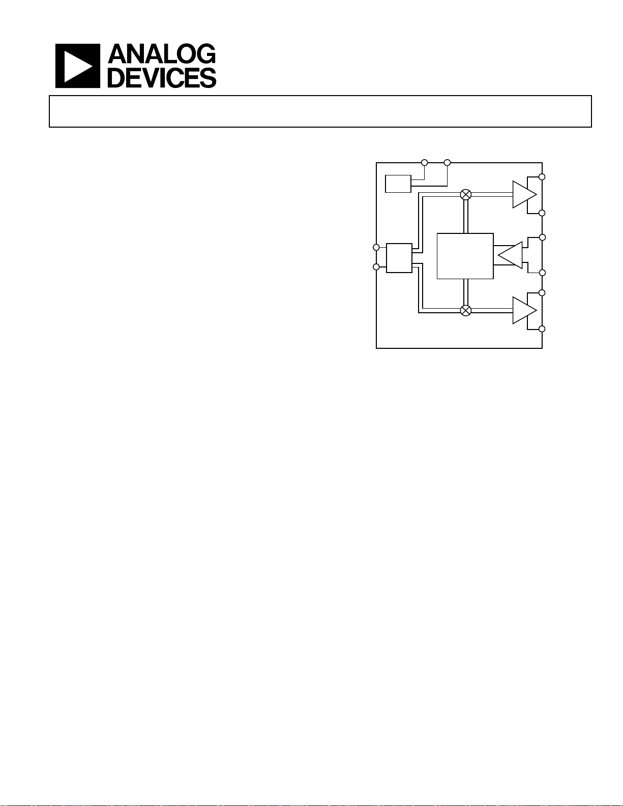
Quadrature Demodulator
ADL5380
FUNCTIONAL BLOCK DIAGRAM
ENBL ADJ
ADL5380
BIAS
RFIN
V2I
RFIP
QUADRATURE
PHASE SPLITTER
Figure 1.
IHI
ILO
LOIP
LOIN
QHI
QLO
07585-001
GENERAL DESCRIPTION
The ADL5380 is a broadband quadrature I-Q demodulator that
covers an RF/IF input frequency range from 400 MHz to 6 GHz.
With a NF = 10.9 dB, IP1dB = 11.6 dBm, and IIP3 = 29.7 dBm @
900 MHz, the ADL5380 demodulator offers outstanding dynamic
range suitable for the demanding infrastructure direct-conversion
requirements. The differential RF inputs provide a well-behaved
broadband input impedance of 50 and are best driven from a
1:1 balun for optimum performance.
Excellent demodulation accuracy is achieved with amplitude
and phase balances of ~0.07 dB and ~0.2°, respectively. The
demodulated in-phase (I) and quadrature (Q) differential outputs
are fully buffered and provide a voltage conversion gain of ~7 dB.
The buffered baseband outputs are capable of driving a 2 V p-p
differential signal into 200 .
Rev. 0
Information furnished by Analog Devices is believed to be accurate and reliable. However, no
responsibility is assumed by Analog Devices for its use, nor for any infringements of patents or other
rights of third parties that may result from its use. Specifications subject to change without notice. No
license is granted by implication or otherwise under any patent or patent rights of Analog Devices.
Trademarks and registered trademarks are the property of their respective owners.
The fully balanced design minimizes effects from second-order
distortion. The leakage from the LO port to the RF port is
<−50 dBm. Differential dc offsets at the I and Q outputs are
typically <20 mV. Both of these factors contribute to the
excellent IIP2 specification, which is >65 dBm.
The ADL5380 operates off a single 4.75 V to 5.25 V supply. The
supply current is adjustable by placing an external resistor from
the ADJ pin to either the positive supply, V
, (to increase supply
S
current and improve IIP3) or to ground (which decreases supply
current at the expense of IIP3).
The ADL5380 is fabricated using the Analog Devices, Inc.,
advanced silicon-germanium bipolar process and is available
in a 24-lead exposed paddle LFCSP.
One Technology Way, P.O. Box 9106, Norwood, MA 02062-9106, U.S.A.
Tel: 781.329.4700 www.analog.com
Fax: 781.461.3113 ©2009 Analog Devices, Inc. All rights reserved.
Page 2

ADL5380
TABLE OF CONTENTS
Features .............................................................................................. 1
Applications ....................................................................................... 1
Functional Block Diagram .............................................................. 1
General Description ......................................................................... 1
Revision History ............................................................................... 2
Specifications ..................................................................................... 3
Absolute Maximum Ratings ............................................................ 5
ESD Caution .................................................................................. 5
Pin Configuration and Function Descriptions ............................. 6
Typical Performance Characteristics ............................................. 7
Low Band Operation .................................................................... 7
Midband Operation ................................................................... 11
High Band Operation ................................................................ 14
Distributions for fLO = 900 MHz ............................................... 17
Distributions for fLO = 1900 MHz ............................................. 18
Distributions for fLO = 2700 MHz ............................................. 19
Distributions for fLO = 3600 MHz ............................................. 20
Distributions for fLO = 5800 MHz ............................................. 21
Circuit Description ......................................................................... 22
LO Interface................................................................................. 22
V-to-I Converter ......................................................................... 22
Mixers .......................................................................................... 22
Emitter Follower Buffers ........................................................... 22
Bias Circuit .................................................................................. 22
Applications Information .............................................................. 23
Basic Connections ...................................................................... 23
Power Supply ............................................................................... 23
Local Oscillator (LO) Input ...................................................... 23
RF Input ....................................................................................... 24
Baseband Outputs ...................................................................... 24
Error Vector Magnitude (EVM) Performance ........................... 24
Low IF Image Rejection ............................................................. 25
Example Baseband Interface ..................................................... 26
Characterization Setups ................................................................. 30
Evaluation Board ............................................................................ 32
Thermal Grounding and Evaluation Board Layout ............... 34
Outline Dimensions ....................................................................... 35
Ordering Guide .......................................................................... 35
REVISION HISTORY
7/09—Revision 0: Initial Version
Rev. 0 | Page 2 of 36
Page 3

ADL5380
SPECIFICATIONS
VS = 5 V, TA = 25°C, fLO = 900 MHz, fIF = 4.5 MHz, PLO = 0 dBm, ZO = 50 Ω, unless otherwise noted. Baseband outputs differentially
loaded with 450 Ω. Loss of the balun used to drive the RF port was de-embedded from these measurements.
Table 1.
Parameter Condition Min Typ Max Unit
OPERATING CONDITIONS
LO and RF Frequency Range 0.4 6 GHz
LO INPUT LOIP, LOIN
Input Return Loss LO driven differentially through a balun at 900 MHz −10 dB
LO Input Level −6 0 +6 dBm
I/Q BASEBAND OUTPUTS QHI, QLO, IHI, ILO
Voltage Conversion Gain 450 Ω differential load on I and Q outputs at 900 MHz 6.9 dB
200 Ω differential load on I and Q outputs at 900 MHz 5.9 dB
Demodulation Bandwidth 1 V p-p signal, 3 dB bandwidth 390 MHz
Quadrature Phase Error At 900 MHz 0.2 Degrees
I/Q Amplitude Imbalance 0.07 dB
Output DC Offset (Differential) 0 dBm LO input at 900 MHz ±10 mV
Output Common Mode Dependent on ADJ pin setting
V
V
V
0.1 dB Gain Flatness 37 MHz
Output Swing Differential 200 Ω load 2 V p-p
Peak Output Current Each pin 12 mA
POWER SUPPLIES VS = VCC1, VCC2, VCC3
Voltage 4.75 5.25 V
Current 1.5 kΩ from ADJ pin to VS; ENBL pin low 245 mA
1.5 kΩ from ADJ pin to VS; ENBL pin high 145 mA
ENABLE FUNCTION Pin ENBL
Off Isolation −70 dB
Turn-On Settling Time ENBL high to low 45 ns
Turn-Off Settling Time ENBL low to high 950 ns
ENBL High Level (Logic 1) 2.5 V
ENBL Low Level (Logic 0) 1.7 V
DYNAMIC PERFORMANCE at RF = 900 MHz V
Conversion Gain 6.9 dB
Input P1dB 11.6 dBm
RF Input Return Loss RFIP, RFIN driven differentially through a balun −19 dB
Second-Order Input Intercept (IIP2) −5 dBm each input tone 68 dBm
Third-Order Input Intercept (IIP3) −5 dBm each input tone 29.7 dBm
LO to RF RFIN, RFIP terminated in 50 Ω −52 dBm
RF to LO LOIN, LOIP terminated in 50 Ω −67 dBc
IQ Magnitude Imbalance 0.07 dB
IQ Phase Imbalance 0.2 Degrees
Noise Figure 10.9 dB
Noise Figure Under Blocking Conditions With a −5 dBm input interferer 5 MHz away 13.1 dB
~ 4 V (set by 1.5 kΩ from ADJ pin to VS) VS − 2.5 V
ADJ
~ 4.8 V (set by 200 Ω from ADJ pin to VS) VS − 2.8 V
ADJ
~ 2.4 V (ADJ pin open) VS − 1.2 V
ADJ
~ 4 V (set by 1.5 kΩ from ADJ pin to VS)
ADJ
Rev. 0 | Page 3 of 36
Page 4

ADL5380
Parameter Condition Min Typ Max Unit
DYNAMIC PERFORMANCE at RF = 1900 MHz V
Conversion Gain 6.8 dB
Input P1dB 11.6 dBm
RF Input Return Loss RFIP, RFIN driven differentially through a balun −13 dB
Second-Order Input Intercept (IIP2) −5 dBm each input tone 61 dBm
Third-Order Input Intercept (IIP3) −5 dBm each input tone 27.8 dBm
LO to RF RFIN, RFIP terminated in 50 Ω −49 dBm
RF to LO LOIN, LOIP terminated in 50 Ω −77 dBc
IQ Magnitude Imbalance 0.07 dB
IQ Phase Imbalance 0.25 Degrees
Noise Figure 11.7 dB
Noise Figure Under Blocking Conditions With a −5 dBm input interferer 5 MHz away 14 dB
DYNAMIC PERFORMANCE at RF = 2700 MHz V
Conversion Gain 7.4 dB
Input P1dB 11 dBm
RF Input Return Loss RFIP, RFIN driven differentially through a balun −10 dB
Second-Order Input Intercept (IIP2) −5 dBm each input tone 54 dBm
Third-Order Input Intercept (IIP3) −5 dBm each input tone 28 dBm
LO to RF RFIN, RFIP terminated in 50 Ω −49 dBm
RF to LO LOIN, LOIP terminated in 50 Ω −73 dBc
IQ Magnitude Imbalance 0.07 dB
IQ Phase Imbalance 0.5 Degrees
Noise Figure 12.3 dB
DYNAMIC PERFORMANCE at RF = 3600 MHz V
Conversion Gain 6.3 dB
Input P1dB 9.6 dBm
RF Input Return Loss RFIP, RFIN driven differentially through a balun −11 dB
Second-Order Input Intercept (IIP2) −5 dBm each input tone 48 dBm
Third-Order Input Intercept (IIP3) −5 dBm each input tone 21 dBm
LO to RF RFIN, RFIP terminated in 50 Ω −46 dBm
RF to LO LOIN, LOIP terminated in 50 Ω −72 dBc
IQ Magnitude Imbalance 0.14 dB
IQ Phase Imbalance 1.1 Degrees
Noise Figure 14.2 dB
Noise Figure Under Blocking Conditions With a −5 dBm input interferer 5 MHz away 16.2 dB
DYNAMIC PERFORMANCE at RF = 5800 MHz V
Conversion Gain 5.8 dB
Input P1dB 8.2 dBm
RF Input Return Loss RFIP, RFIN driven differentially through a balun −7.5 dB
Second-Order Input Intercept (IIP2) −5 dBm each input tone 44 dBm
Third-Order Input Intercept (IIP3) −5 dBm each input tone 20.6 dBm
LO to RF RFIN, RFIP terminated in 50 Ω −47 dBm
RF to LO LOIN, LOIP terminated in 50 Ω −62 dBc
IQ Magnitude Imbalance 0.07 dB
IQ Phase Imbalance −1.25 Degrees
Noise Figure 15.5 dB
Noise Figure Under Blocking Conditions With a −5 dBm input interferer 5 MHz away 18.9 dB
~ 4 V (set by 1.5 kΩ from ADJ pin to VS)
ADJ
~ 4 V (set by 1.5 kΩ from ADJ pin to VS)
ADJ
~ 4.8 V (set by200 Ω from ADJ pin to VS)
ADJ
~ 2.4 V (ADJ pin left open)
ADJ
Rev. 0 | Page 4 of 36
Page 5

ADL5380
ABSOLUTE MAXIMUM RATINGS
Table 2.
Parameter Rating
Supply Voltage: VCC1, VCC2, VCC3 5.5 V
LO Input Power 13 dBm (re: 50 Ω)
RF Input Power 15 dBm (re: 50 Ω)
Internal Maximum Power Dissipation 1370 mW
1
θ
53°C/W
JA
Maximum Junction Temperature 150°C
Operating Temperature Range −40°C to +85°C
Storage Temperature Range −65°C to +125°C
1
Per JDEC standard JESD 51-2. For information on optimizing thermal
impedance, see the Thermal Grounding and Evaluation Board Layout
section.
Stresses above those listed under Absolute Maximum Ratings
may cause permanent damage to the device. This is a stress
rating only; functional operation of the device at these or any
other conditions above those indicated in the operational
section of this specification is not implied. Exposure to absolute
maximum rating conditions for extended periods may affect
device reliability.
ESD CAUTION
Rev. 0 | Page 5 of 36
Page 6

ADL5380
2
A
PIN CONFIGURATION AND FUNCTION DESCRIPTIONS
RFIN
RFIP
GND3
VCC3
GND3
ADJ
02
91
12
22
32
42
PIN 1
INDICATOR
1GND3
2GND1
ADL5380
3IHI
TOP VIEW
4ILO
(Not to Scale)
5GND1
6VCC1
9
7
8
LOIP
ENBL
GND4
NOTES
1. NC = NO CONNECT .
. THE EXPO SED PAD SHOULD BE CO NNECTED TO
LOW IMPEDANCE THERMAL AND EL ECTRICAL
GROUND PLANE.
Figure 2. Pin Configuration
Table 3. Pin Function Descriptions
Pin No. Mnemonic Description
1, 2, 5, 8, 11, 14,
GND1, GND2, GND3, GND4 Ground Connect.
17, 18, 20, 23
3, 4, 15, 16 IHI, ILO, QLO, QHI
I Channel and Q Channel Mixer Baseband Outputs. These outputs have a 50 Ω differential
output impedance (25 Ω per pin). Each output pair can swing 2 V p-p (differential) into a
load of 200 Ω. The output 3 dB bandwidth is ~400 MHz.
6, 13, 24 VCC1, VCC2, VCC3
Supply. Positive supply for LO, IF, biasing, and baseband sections. Decouple these pins to
the board ground using the appropriate-sized capacitors.
7 ENBL
Enable Control. When pulled low, the part is fully enabled; when pulled high, the part is
partially powered down and the output is disabled.
9, 10 LOIP, LOIN
Local Oscillator Input. Pins must be ac-coupled. A differential drive through a balun is
necessary to achieve optimal performance. Recommended balun is the Mini-Circuits
TC1-1-13 for lower frequencies, the Johanson Technology 3600 balun for midband
frequencies, and the Johanson Technology 5400 balun for high band frequencies.
Balun choice depends on the desired frequency range of operation.
12 NC Do not connect this pin.
19 ADJ
A resistor to V
that optimizes third-order intercept. For operation <3 GHz, R
S
For operation from 3 GHz to 4 GHz, R
See the Circuit Description section for more details.
21, 22 RFIN, RFIP
RF Input. A single-ended 50 Ω signal can be applied differentially to the RF inputs through
a 1:1 balun. Recommended balun is the Mini-Circuits TC1-1-13 for lower frequencies, the
Johanson Technology 3600 balun for midband frequencies, and the Johanson Technology
5400 balun for high band frequencies. Balun choice depends on the desired frequency
range of operation.
EP Exposed Paddle. Connect to a low impedance thermal and electrical ground plane.
18 G ND3
17 G ND2
16 Q HI
15 Q LO
14 G ND2
13 VCC2
11
21
01
NC
LOIN
GND4
07585-002
= 1.5 kΩ.
= 200 Ω. For operation >5 GHz, R
ADJ
ADJ
= open.
ADJ
Rev. 0 | Page 6 of 36
Page 7
ADL5380
TYPICAL PERFORMANCE CHARACTERISTICS
VS = 5 V, TA = 25°C, LO drive level = 0 dBm, RF input balun loss is de-embedded, unless otherwise noted.
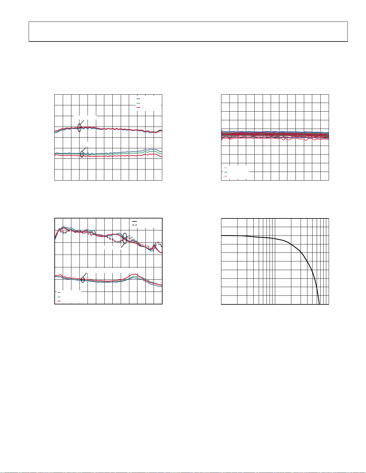
LOW BAND OPERATION
RF = 400 MHz to 3 GHz; Mini-Circuits TC1-1-13 balun on LO and RF inputs, 1.5 kΩ from the ADJ pin to VS.
18
16
14
12
10
8
GAIN (dB), IP1dB (dBm)
6
4
2
400
600
INPUT P1dB
GAIN
800
1000
1200
LO FREQUENCY (MHz)
1400
1600
1800
2000
2200
TA = –40°C
T
= +25°C
A
T
= +85°C
A
2600
2400
2800
3000
Figure 3. Conversion Gain and Input 1 dB Compression Point (IP1dB) vs.
LO Frequency
80
70
60
50
40
IIP3, IIP2 (dBm)
30
20
TA = –40°C
T
= +25°C
A
T
= +85°C
A
10
400
600
800
1000
INPUT IP2
INPUT IP3 ( I AND Q CHANNELS)
1200
1400
1600
LO FREQUENCY (MHz)
1800
2000
2200
I CHANNEL
Q CHANNEL
2600
2400
2800
3000
Figure 4. Input Third-Order Intercept (IIP3) and
Input Second-Order Intercept Point (IIP2) vs. LO Frequency
07585-003
07585-004
1.0
0.8
0.6
0.4
0.2
0
–0.2
–0.4
GAIN MISMATCH (dB)
–0.6
TA = –40°C
–0.8
T
= +25°C
A
T
= +85°C
–1.0
A
400
600
800
1000
1200
1400
1600
1800
2200
2000
LO FREQUENCY (MHz)
2400
Figure 5. IQ Gain Mismatch vs. LO Frequency
2
1
0
–1
–2
–3
–4
–5
BASEBAND RESPONSE (dB)
–6
–7
–8
10 100 1000
BASEBAND FREQUENCY (M Hz)
Figure 6. Normalized IQ Baseband Frequency Response
2600
2800
3000
07585-005
07585-006
Rev. 0 | Page 7 of 36
Page 8
ADL5380
d
18
TA = –40°C
T
17
16
15
14
13
12
NOISE FI GURE (dB)
11
10
= +25°C
A
T
= +85°C
A
9
8
400
600
800
1000
1200
1400
1600
1800
2200
2400
2600
LO FREQUENCY (MHz)
2000
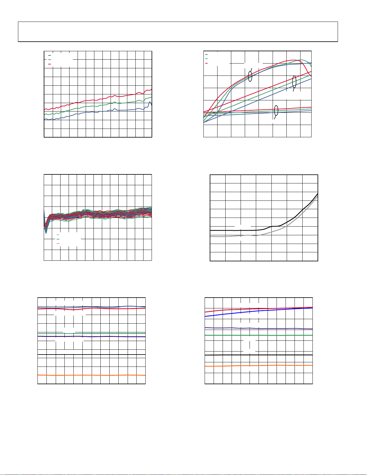
Figure 7. Noise Figure vs. LO Frequency
4
3
2
1
0
–1
TA = –40°C
T
600
= +25°C
A
T
= +85°C
A
800
1000
1200
1400
1600
1800
LO FREQUE NCY (MHz)
2000
2200
2400
2600
QUADRATURE PHASE ERRO R (Degrees)
–2
–3
–4
400
Figure 8. IQ Quadrature Phase Error vs. LO Frequency
20
18
16
14
12
10
8
6
4
2
GAIN (dB), IP1dB (dBm), NOISE FIGURE (d B)
0
–6–5–4–3–2–10123456
IIP2, I CHANNEL
IIP2, Q CHANNEL
IP1dB
NOISE FI GURE
GAIN
IIP3
LO LEVEL (dBm)
Figure 9. Conversion Gain, IP1dB, Noise Figure, IIP3, and IIP2 vs.
LO Level, f
= 900 MHz
LO
2800
2800
35
TA = –40°C
T
= +25°C
A
T
= +85°C
30
A
25
20
15
10
IIP3 (dBm) AND NOISE FI GURE (dB)
5
0
3000
07585-007
1.0 1. 5 2. 0 2. 5 3.0 3.5 4. 0 4. 5
Figure 10. IIP3, Noise Figure, and Supply Current vs. V
INPUT IP3
V
ADJ
NOISE FI GURE
(V)
SUPPLY
CURRENT
ADJ
25
23
21
19
B)
17
15
3000
13
NOISE FIGURE (
11
9
7
5
–30 –25 –20 –15 –10 –5 0 5
07585-008
Figure 11. Noise Figure vs. Input Blocker Level, f
1920MHz
920MHz
RF BLOCKER INPUT POW ER (dBm)
= 900 MHz, fLO = 1900 MHz
LO
(RF Blocker 5 MHz Offset)
75
70
65
60
55
50
45
IIP3, IIP2 ( dBm)
40
35
30
25
7585-009
18
16
14
12
10
8
6
4
GAIN (dB), IP1dB (dBm), NOISE FIGURE (dB)
2
–6–5–4–3–2–10123456
IIP2, Q CHANNEL
IIP2, I CHANNEL
NOISE FIGURE
IP1dB
GAIN
IIP3
LO LEVEL (dBm)
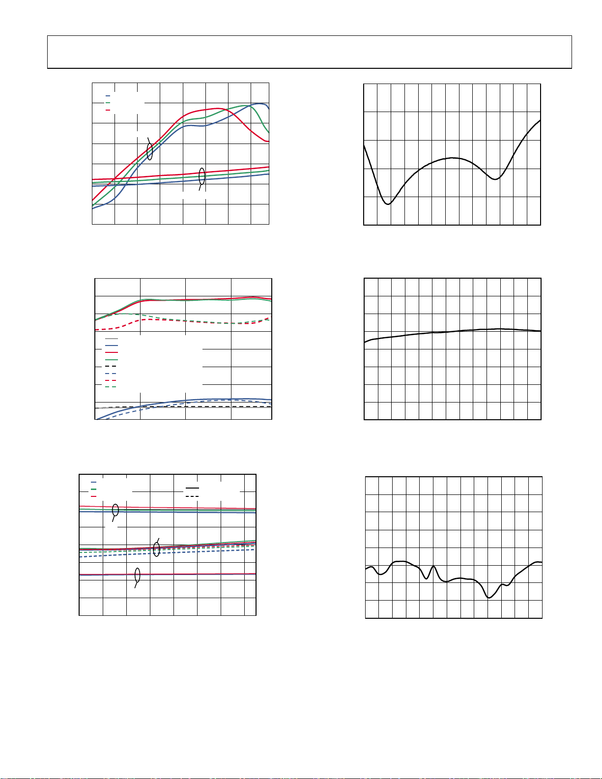
Figure 12. Conversion Gain, IP1dB, Noise Figure, IIP3, and IIP2 vs.
LO Level, f
= 2700 MHz
LO
300
280
260
240
220
200
180
160
, fLO = 900 MHz
60
55
50
45
40
35
30
25
20
SUPPLY CURRENT (mA)
07585-010
07585-011
IIP3, IIP2 (dBm)
07585-012
Rev. 0 | Page 8 of 36
Page 9
ADL5380
A
–
d
m
–
35
TA = –40°C
T
30
25
20
= +25°C
A
T
= +85°C
A
INPUT IP3
0
–5
–10
15
10
IIP3 (dBm) AND NOISE FI GURE (dB)
5
0
1.0 1.5 2.0 2.5 3.0 3.5 4.0 4.5
Figure 13. IIP3 and Noise Figure vs. V
NOISE FI GURE
V
(V)
ADJ
, fLO = 2700 MHz
ADJ
80
70
60
50
40
30
IN (dB), IP1dB (dBm), IIP2
20
I AND Q CHANNELS (dBm)
G
10
0
900MHz: GAIN
900MHz: IP1d B
900MHz: IIP2, I CHANNEL
900MHz: IIP2, Q CHANNEL
2700MHz: GAIN
2700MHz: IP1d B
2700MHz: IIP2, I CHANNEL
2700MHz: IIP2, Q CHANNEL
1234
V
(V)
ADJ
Figure 14. Conversion Gain, IP1dB, and IIP2 vs.
, fLO = 900 MHz, fLO = 2700 MHz
V
ADJ
40
35
30
25
20
15
IP1dB, IIP3 (dBm)
10
TA = –40°C
T
= +25°C
A
T
= +85°C
A
IIP3
5
0
4.5 6 .5 8.5 10.5 12.5 14. 5 16. 5 18.5
BASEBAND FREQUENCY (M Hz)
IIP2
IP1dB
I CHANNEL
Q CHANNEL
Figure 15. IP1dB, IIP3, and IIP2 vs. Baseband Frequency
–15
RETURN LOSS ( dB)
–20
–25
0.40.60.81.01.21.41.61.82.02.22.42.62.83.0
07585-013
RF FREQ UENCY (GHz)
07585-016
Figure 16. RF Port Return Loss vs. RF Frequency Measured on
Characterization Board Through TC1-1-13 Balun
20
–30
–40
)
–50
B
–60
–70
LEAKAGE (
–80
–90
–100
0.4 0.6 0.8 1.0 1.2 1.4 1.6 1.8 2.0 2.2 2.4 2.6 2.8 3.0
07585-014
LO FREQUENCY (GHz)
07585-017
Figure 17. LO-to-RF Leakage vs. LO Frequency
90
85
80
75
70
65
60
IIP2, I AND Q CHANNELS (dBm)
55
50
07585-015
20
–30
–40
–50
–60
–70
LEAKAGE (dBc)
–80
–90
–100
0.4 0.6 0.8 1.0 1.2 1.4 1.6 1.8 2.0 2.2 2.4 2.6 2.8 3.0
RF FREQUENCY ( GHz)
07585-018
Figure 18. RF-to-LO Leakage vs. RF Frequency
Rev. 0 | Page 9 of 36
Page 10
ADL5380
0
–2
–4
–6
–8
–10
RETURN LOSS ( dB)
–12
–14
–16
0.4 0.6 0.8 1.0 1.2 1.4 1.6 1.8 2.0 2.2 2.4 2.6 2.8 3.0
LO FREQUENCY (GHz)
Figure 19. LO Port Return Loss vs. LO Frequency Measured on
Characterization Board Through TC1-1-13 Balun
07585-019
Rev. 0 | Page 10 of 36
Page 11
ADL5380
d
R
MIDBAND OPERATION
RF = 3 GHz to 4 GHz; Johanson Technology 3600BL14M050T balun on LO and RF inputs, 200 Ω from V
14
13
12
11
10
GAIN (dB), IP1dB (dBm)
IP1dB
9
8
7
6
5
4
3.03.13.23.33.43.53.63.73.83.94.0
GAIN
LO FREQUENCY (GHz)
TA = –40°C
T
= +25°C
A
T
= +85°C
A
07585-020
Figure 20. Conversion Gain and Input 1 dB Compression Point (IP1dB) vs.
LO Frequency
80
TA = –40°C
T
= +25°C
A
70
T
= +85°C
A
60
50
40
IIP3, IIP2 (dBm)
30
20
10
3.0 3.1 3.2 3.3 3.4 3.5 3.6 3. 7 3. 8 4.03.9
INPUT IP3 I AND Q CHANNELS
INPUT IP2
LO FREQUENCY (GHz)
I CHANNEL
Q CHANNEL
07585-021
Figure 21. Input Third-Order Intercept (IIP3) and
Input Second-Order Intercept Point (IIP2) vs. LO Frequency
1.0
TA = –40°C
0.8
T
= +25°C
A
T
0.6
0.4
0.2
0
–0.2
GAIN MISMATCH (dB)
–0.4
–0.6
–0.8
–1.0
= +85°C
A
3.0 3.2 3.4 3.6 3.8 4. 0
LO FREQUENCY (GHz)
Figure 22. IQ Gain Mismatch vs. LO Frequency
7585-022
20
18
IIP2, I CHANNEL
16
14
12
10
8
6
4
2
GAIN (dB), IP1dB (dBm), NOISE FIGURE (dB)
0
–6–5–4–3–2–1 0123456
IIP2, Q CHANNEL
NOISE FI GURE
IP1dB
GAIN
IIP3
LO LEVEL (dBm)
Figure 23. Conversion Gain, IP1dB, Noise Figure, IIP3, and IIP2 vs.
LO Level, f
18
17
16
15
B)
14
13
12
TA = –40°C
T
= +25°C
NOISE FIGURE (
11
10
A
T
= +85°C
A
9
8
3.0 3.1 3. 2 3. 3 3. 4 3. 5 3. 6 3. 7 3. 8 3. 9 4. 0
LO FREQUENCY (GHz)
Figure 24. Noise Figure vs. LO Frequency
4
TA = –40°C
T
= +25°C
A
T
= +85°C
A
3.0 3.2 3.4 3.6 3.8
LO FREQUENCY (GHz)
OR (Degrees)
–1
QUADRATURE PHASE ER
3
2
1
0
–2
–3
–4
Figure 25. IQ Quadrature Phase Error vs. LO Frequency
to VS.
ADJ
= 3600 MHz
LO
60
55
50
45
40
35
30
25
20
15
10
3.93.1 3.3 3.5 3.7 4.0
IIP3, IIP2 (dBm)
07585-024
07585-025
07585-023
Rev. 0 | Page 11 of 36
Page 12

ADL5380
A
–
–
30
25
INPUT IP3
20
TA = –40°C
= +25°C
T
A
= +85°C
T
A
300
280
260
20
–30
–40
15
10
5
IIP3 (dBm) AND NOISE FI GURE (dB)
SUPPLY CURRENT
0
1.01.52.02.53.03.54.04.5
V
(V)
ADJ
Figure 26. IIP3, Noise Figure, and Supply Current vs. V
NOISE FI GURE
ADJ
25
23
21
19
17
NOISE FI GURE (dB)
15
13
11
–30 –25 –20 –15 –10 –5 0 5
RF POWEL LEVEL (dBm)
Figure 27. Noise Figure vs. Input Blocker Level, fLO = 3600 MHz
(RF Blocker 5 MHz Offset)
80
70
60
50
40
30
20
IN (dB), IP1dB (dBm), IIP2
I AND Q CHANNELS (dBm)
G
10
0
–10
Figure 28. Conversion Gain, IP1dB, and IIP2 vs. V
3600MHz: GAIN
3600MHz: IP1d B
3600MHz: IIP2, I CHANNEL
3600MHz: IIP2, Q CHANNEL
1234
V
(V)
ADJ
, fLO = 3600 MHz
ADJ
240
220
200
180
, fLO = 3600 MHz
07585-027
–50
CURRENT (mA)
7585-026
LEAKAGE (dBm)
–60
–70
–80
3.1 3.2 3.3 3.4 3.5 3.6 3.7 3.8 3.9 4.0
LO FREQUE NCY (GHz)
07585-029
Figure 29. LO-to-RF Leakage vs. LO Frequency
20
–30
–40
–50
–60
–70
LEAKAGE (d Bc)
–80
–90
–100
3.1 3.2 3.3 3.4 3.5 3.6 3.7 3.8 3.9 4.0
RF FREQUENCY ( GHz)
07585-030
Figure 30. RF-to-LO Leakage vs. RF Frequency
0
–2
–4
–6
–8
RETURN LOSS (d B)
–10
–12
3.1 3.2 3.3 3.4 3.5 3.6 3.7 3.8 3.9 4.0
07585-028
RF FREQUENCY ( GHz)
07585-031
Figure 31. RF Port Return Loss vs. RF Frequency Measured on
Characterization Board Through Johanson Technology 3600 Balun
Rev. 0 | Page 12 of 36
Page 13

ADL5380
0
–5
–10
–15
–20
RETURN LOSS ( dB)
–25
–30
3.1 3.2 3.3 3.4 3.5 3.6 3.7 3.8 3.9 4. 0
LO FREQUENCY (GHz)
Figure 32. LO Port Return Loss vs. LO Frequency Measured on
Characterization Board Through Johanson Technology 3600 Balun
7585-032
Rev. 0 | Page 13 of 36
Page 14

ADL5380
A
HIGH BAND OPERATION
RF = 5 GHz to 6 GHz; Johanson Technology 5400BL15B050E balun on LO and RF inputs, the ADJ pin is open.
12
11
10
9
8
7
6
5
GAIN (dB), INPUT P1dB (dBm)
TA = –40°C
4
T
= +25°C
A
T
3
2
= +85°C
A
5.1 5.2 5.3 5.4 5.5 5.6 5.7 5.8 5.9 6.0
INPUT P1dB
LO FREQUENCY (GHz)
GAIN
7585-033
Figure 33. Conversion Gain and Input 1 dB Compression Point (IP1dB) vs.
LO Frequency
80
TA = –40°C
70
T
= +25°C
A
T
= +85°C
A
60
50
40
IIP3, IIP2 (dBm)
INPUT IP3 (I AND Q CHANNELS)
30
20
10
5.1 5.2 5.3 5.4 5.5 5.6 5.7 5.8 5.9 6.0
LO FREQUENCY (GHz)
INPUT IP2
I CHANNEL
Q CHANNEL
07585-034
Figure 34. Input Third-Order Intercept (IIP3) and
Input Second-Order Intercept Point (IIP2) vs. LO Frequency
1.0
0.8
0.6
0.4
0.2
–0.2
–0.4
–0.6
IQ AMPLI TUDE MISMATCH (dB)
–0.8
–1.0
TA = –40°C
T
= +25°C
A
T
= +85°C
A
0
5.15.25.35.45.55.65.75.85.96.0
LO FREQUENCY (GHz)
07585-035
Figure 35. IQ Gain Mismatch vs. LO Frequency
20
18
IIP2, Q CHANNEL
16
14
12
10
8
6
4
2
GAIN (dB), IP1dB (dBm), NOISE FIGURE (dB)
0
–6 –5 –4 –3 –2 –1 0 1 2 3 4 5 6
NOISE FI GURE
IIP2, I CHANNEL
IP1dB
GAIN
IIP3
LO LEVEL (dBm)
Figure 36. Conversion Gain, IP1dB, Noise Figure, IIP3, and IIP2 vs.
LO Level, f
20
TA = –40°C
19
18
17
16
15
14
13
12
NOISE FI GURE (dB)
11
10
9
8
= –25°C
T
A
= +85°C
T
A
5.0 5.1 5.2 5.3 5.4 5.5 5.6 5.7 5.8 5.9 6.0
= 5800 MHz
LO
LO FREQUENCY (GHz)
Figure 37. Noise Figure vs. LO Frequency
4
3
2
1
TCH (Degrees)
0
–1
–2
IQ PHASE MIS M
–3
–4
TA = –40°C
= +25°C
T
A
= +85°C
T
A
5.1 5.2 5.3 5.4 5.5 5.6 5.7 5.8 5.9 6.0
LO FREQUENCY (GHz)
Figure 38. IQ Quadrature Phase Error vs. LO Frequency
60
55
50
45
40
35
30
IIP3, IIP2 (dBm)
25
20
15
10
07585-036
07585-037
07585-038
Rev. 0 | Page 14 of 36
Page 15

ADL5380
–
d
m
–
L
30
25
20
NOISE FI GURE
15
INPUT IP3
TA = –40°C
= +25°C
T
A
= +85°C
T
A
300
280
260
240
20
–30
–40
)
–50
B
–60
10
5
IIP3 (dBm) AND NOISE FI GURE (dB)
0
1.01.52.02.53.03.54.04.5
Figure 39. IIP3, Noise Figure, and Supply Current vs. V
SUPPLY CURRENT
V
(V)
ADJ
ADJ
25
20
15
10
NOISE FIGURE (dB)
5
0
–30 –25 –20 –15 –10 –5
RF POWER LEVEL (dBm)
Figure 40. Noise Figure vs. Input Blocker Level, fLO = 5800 MHz
(RF Blocker 5 MHz Offset)
60
220
200
180
, fLO = 5800 MHz
07585-040
CURRENT (mA)
7585-039
–70
LEAKAGE (
–80
–90
–10 0
5.1 5.2 5.3 5.4 5.5 5. 6 5.7 5.8 5.9 6.0
LO FREQUENC Y ( GHz)
07585-042
Figure 42. LO-to-RF Leakage vs. LO Frequency
20
–30
–40
–50
–60
–70
LEAKAGE (dBc)
–80
–90
–100
RF FREQUENCY ( MHz)
5.75.65.55.45.35.25. 1 5.8 5.9 6.0
07585-043
Figure 43. RF-to-LO Leakage vs. RF Frequency
0
50
40
5800MHz: GAIN
30
20
I AND Q CHANNEL (dBm)
GAIN (dB), IP1dB (dBm), IIP2
10
0
5800MHz: IP1d B
5800MHz: IIP2, I CHANNEL
5800MHz: IIP2, Q CHANNEL
1234
V
(V)
ADJ
Figure 41. Conversion Gain, IP1dB, and IIP2 vs.
R
, fLO = 5800 MHz
BIAS
07585-041
–2
–4
–6
OSS (dB)
–8
–10
RETURN
–12
–14
–16
5.1 5. 2 5.3 5. 4 5.5 5.6 5.7 5.8 5.9 6.0
RF FREQUENCY (GHz)
Figure 44. RF Port Return Loss vs. RF Frequency Measured on
Characterization Board Through Johanson Technology 5400 Balun
07585-044
Rev. 0 | Page 15 of 36
Page 16

ADL5380
–
0
–2
–4
–6
–8
–10
RETURN LOSS (dB)
–12
–14
–16
5.1 5.2 5.3 5.4 5.5 5.6 5.7 5.8 5.9 6.0
LO FREQUENCY (GHz)
Figure 45. LO Port Return Loss vs. LO Frequency Measured on
Characterization Board Through Johanson Technology 5400 Balun
07585-045
Rev. 0 | Page 16 of 36
Page 17

ADL5380
%
%
%
DISTRIBUTIONS FOR fLO = 900 MHz
100
90
80
70
60
50
40
30
20
DISTRIBUTI ON PERCENTAG E (%)
10
0
28 2 9 30 31 32 33 34
INPUT IP3 (dBm)
TA = –40°C
T
= +25°C
A
T
= +85°C
A
07585-046
Figure 46. IIP3 Distributions
100
90
)
80
70
60
50
40
30
20
DISTRIBUTION PERCENT AGE (
10
0
4567891011121314
GAIN (dB), IP1dB (dBm)
IP1dB
GAIN
TA = –40°C
T
= +25°C
A
T
= +85°C
A
07585-047
Figure 47. Gain and IP1dB Distributions
100
90
80
70
60
50
40
30
20
DISTRIBUTI ON PERCENTAG E (%)
10
0
–0.3 –0.2 –0.1 0 0.1 0.2 0.3
TA = –40°C
T
= +25°C
A
T
= +85°C
A
GAIN MIS MATCH (dB)
07585-048
Figure 48. IQ Gain Mismatch Distributions
Rev. 0 | Page 17 of 36
100
90
)
80
70
60
50
40
30
20
DISTRIBUTI ON PERCENTAG E (
10
0
45 50 55 60 65 70 75 80 85
TA = –40°C
T
= +25°C
A
T
= +85°C
A
I CHANNEL
Q CHANNEL
INPUT IP2 (dBm)
Figure 49. IIP2 Distributions for I Channel and Q Channel
100
90
80
70
60
50
40
30
20
DISTRI BUTION PERCE NTAGE (%)
10
0
9.5 10.0 10. 5 11.0 11.5 12.0 12.5
NOISE FIGURE (dB)
TA = –40°C
= +25°C
T
A
= +85°C
T
A
Figure 50. Noise Figure Distributions
100
90
)
80
70
60
50
40
30
20
DISTRIBUTION PERCENTAGE (
10
0
–1.0 –0.8 –0.6 –0.4 –0. 2 0 0.2 0.4 0.6 0.8 1.0
TA = –40°C
= +25°C
T
A
= +85°C
T
A
QUADRATURE PHASE ERROR (Degrees)
Figure 51. IQ Quadrature Phase Error Distributions
07585-049
07585-050
07585-051
Page 18

ADL5380
%
%
%
DISTRIBUTIONS FOR fLO = 1900 MHz
100
90
)
80
70
60
50
40
30
20
DISTRIBUTION PERCENT AGE (
10
TA = –40°C
= +25°C
T
A
= +85°C
T
A
0
24 25 26 27 28 29 30 31 32
INPUT IP3 (dBm)
07585-052
Figure 52. IIP3 Distributions
100
90
)
80
70
60
50
40
30
20
DISTRI BUTI ON PERC ENTAGE (
10
0
4567891011121314
TA = –40°C
T
= +25°C
A
T
= +85°C
A
IP1dB
GAIN
GAIN (dB), IP1dB (dBm)
07585-053
Figure 53. Gain and IP1dB Distributions
100
90
)
80
70
60
50
40
30
20
DISTRIBUTI ON PERCENTAG E (
10
0
–0.3 –0.2 – 0.1 0 0. 1 0.2 0.3
TA = –40°C
T
= +25°C
A
T
= +85°C
A
GAIN M ISMATCH (dB)
07585-054
Figure 54. IQ Gain Mismatch Distributions
Rev. 0 | Page 18 of 36
100
90
80
70
60
50
40
30
20
DISTRIBUTION PERCENTAG E (%)
10
0
TA = –40°C
T
= +25°C
A
T
= +85°C
A
I CHANNEL
Q CHANNEL
45 50 55 60 65 70 75 80
INPUT IP2 (dBm)
Figure 55. IIP2 Distributions for I Channel and Q Channel
100
90
80
70
60
50
40
30
20
DISTRIBUTI ON PERCENTAGE (%)
10
0
10.5 11. 0 11.5 12.0 12.5 13. 0 13.5
NOISE FIGURE (dB)
TA = –40°C
T
= +25°C
A
T
= +85°C
A
Figure 56. Noise Figure Distributions
100
90
80
70
60
50
40
30
20
DISTRIBUTI ON PERCENTAG E (%)
10
0
–1.0 –0.8 –0.6 –0.4 –0.2 0 0.2 0.4 0.6 0.8 1 .0
TA = –40°C
T
= +25°C
A
T
= +85°C
A
QUADRATURE PHASE ERRO R (Degrees)
Figure 57. IQ Quadrature Phase Error Distributions
07585-055
07585-056
7585-057
Page 19

ADL5380
DISTRIBUTIONS FOR fLO = 2700 MHz
100
90
80
70
60
50
40
30
20
DISTRIBUTION PERCENTAG E (%)
10
TA = –40°C
T
= +25°C
A
T
= +85°C
A
0
18 20 22 24 26 28 30 32 34 36
INPUT IP3 (dBm)
Figure 58. IIP3 Distributions
100
90
TA = –40°C
= +25°C
T
A
= +85°C
T
80
A
70
60
50
40
30
20
DISTRIBUTION PERCENTAG E (%)
10
0
4567891011121314
GAIN (dB), IP1dB (dBm)
Figure 59. Gain and IP1dB Distributions
100
90
80
70
60
50
40
30
20
DISTRIBUTI ON PERCENTAG E (%)
10
0
–0.3 –0.2 –0.1 0 0.1 0 .2 0.3
TA = –40°C
= +25°C
T
A
= +85°C
T
A
GAIN MISMATCH (dB)
Figure 60. IQ Gain Mismatch Distributions
IP1dB
GAIN
7585-058
07585-059
07585-060
Rev. 0 | Page 19 of 36
100
90
80
70
60
50
40
30
20
DISTRIBUTI ON PERCENTAG E (%)
10
TA = –40°C
T
= +25°C
A
T
= +85°C
A
0
35 40 45 50 55 60 65 70 75
INPUT IP2 (dBm)
I CHANNEL
Q CHANNEL
Figure 61. IIP2 Distributions for I Channel and Q Channel
100
TA = –40°C
= +25°C
T
90
A
= +85°C
T
A
80
70
60
50
40
30
20
DISTRIBUTI ON PERCENTAG E (%)
10
0
10.5 11.0 11.5 12.0 12.5 13. 0 13.5 14.0
NOISE FI GURE (dB)
Figure 62. Noise Figure Distributions
100
90
80
70
60
50
40
30
20
DISTRIBUTI ON PERCENTAG E (%)
10
0
–2.0 –1.5 –1.0 –0. 5 0 0.5 1.0 1.5 2.0
TA = –40°C
= +25°C
T
A
= +85°C
T
A
QUADRATURE PHASE ERRO R (Degrees)
Figure 63. IQ Quadrature Phase Error Distributions
07585-061
07585-062
07585-063
Page 20

ADL5380
%
%
%
%
DISTRIBUTIONS FOR fLO = 3600 MHz
100
90
80
70
60
50
40
30
20
DISTRIBUTI ON PERCENTAGE (%)
10
0
15 17 19 21 23 25 27 29 31 33
INPUT IP3 (dBm)
TA = –40°C
= +25°C
T
A
= +85°C
T
A
Figure 64. IIP3 Distributions
100
90
)
80
70
60
50
40
30
20
DISTRIBUTI ON PERCENT AGE (
10
0
4567891011121314
GAIN (dB), IP1dB (dBm)
IP1dB
GAIN
TA = –40°C
= +25°C
T
A
= +85°C
T
A
Figure 65. Gain and IP1dB Distributions
100
90
)
80
70
60
50
40
30
20
DISTRIBUTION PERCENT AGE (
10
0
–0.3 –0.2 –0.1 0 0.1 0.2 0.3
TA = –40°C
T
= +25°C
A
T
= +85°C
A
GAIN MIS MATCH (dB)
Figure 66. IQ Gain Mismatch Distributions
07585-064
07585-065
07585-066
100
90
)
80
70
60
50
40
30
20
DISTRI BUTION PER CENTAG E (
10
0
35 40 45 50 55 60 65 70
TA = –40°C
= +25°C
T
A
= +85°C
T
A
INPUT IP2 (dBm)
I CHANNEL
Q CHANNEL
Figure 67. IIP2 Distributions for I Channel and Q Channel
100
TA = –40°C
= +25°C
T
90
A
= +85°C
T
A
80
70
60
50
40
30
20
DISTRIBUTI ON PERCENTAG E (%)
10
0
12.5 13.0 13.5 14. 0 14.5 15.0 15.5 16 .0
NOISE FIGURE (dB)
Figure 68. Noise Figure Distributions
100
TA = –40°C
90
T
= +25°C
)
80
70
60
50
40
30
20
DISTRIBUTI ON PERCENT AGE (
10
0
A
T
= +85°C
A
–0.5 0 0.5 1.0 1.5 2.0 2.5
QUADRATURE PHASE ERROR (Degrees)
Figure 69. IQ Quadrature Phase Error Distributions
07585-067
07585-068
7585-069
Rev. 0 | Page 20 of 36
Page 21

ADL5380
%
%
DISTRIBUTIONS FOR fLO = 5800 MHz
100
TA = –40°C
90
T
= +25°C
A
T
80
70
60
50
40
30
20
DISTRIBUTION PERCENTAG E (%)
10
0
= +85°C
A
18 19 20 21 22 23 24
INPUT IP3 (dBm)
Figure 70. IIP3 Distributions
100
90
80
70
60
50
40
30
20
DISTRIBUTION PERCENTAGE (%)
10
TA = –40°C
T
= +25°C
A
T
= +85°C
A
IP1dB
GAIN
0
2345678910
GAIN (dB), IP1dB (dBm)
Figure 71. Gain and IP1dB Distributions
100
90
)
80
70
60
50
40
30
20
DISTRI BUTION PER CENTAG E (
10
0
–0.3 –0.2 –0.1 0 0.1 0.2 0.3
TA = –40°C
= +25°C
T
A
= +85°C
T
A
GAIN MIS MATCH (dB)
Figure 72. IQ Gain Mismatch Distributions
07585-070
07585-071
07585-072
100
90
80
70
60
50
40
30
20
DISTRI BUTION PERCE NTAGE (%)
10
TA = –40°C
T
= +25°C
A
T
= +85°C
A
0
30 35 40 45 50 55 60 65 70
INPUT IP2 (dBm)
I CHANNEL
Q CHANNEL
Figure 73. IIP2 Distributions for I Channel and Q Channel
100
90
TA = –40°C
T
= +25°C
)
80
70
60
50
40
30
20
DISTRIBUTI ON PERCENTAGE (
10
A
T
= +85°C
A
0
13.0 13. 5 14. 0 14.5 15. 0 15. 5 16. 0 16. 5 17. 0 17. 5 18. 0
NOISE FIGURE (dB)
Figure 74. Noise Figure Distributions
100
TA = –40°C
90
T
= +25°C
A
T
= +85°C
A
80
70
60
50
40
30
20
DISTRIBUTION PERCENTAGE (%)
10
0
–3 –2 –1 0 1 2 3
QUADRATURE PHASE ERROR ( Degrees)
Figure 75. IQ Quadrature Phase Error Distributions
07585-073
07585-074
07585-075
Rev. 0 | Page 21 of 36
Page 22

ADL5380
CIRCUIT DESCRIPTION
The ADL5380 can be divided into five sections: the local
oscillator (LO) interface, the RF voltage-to-current (V-to-I)
converter, the mixers, the differential emitter follower outputs,
and the bias circuit. A detailed block diagram of the device is
shown in Figure 76.
ENBL ADJ
RFIN
RFIP
BIAS
V2I
ADL5380
QUADRATURE
PHASE SPLITTER
Figure 76. Block Diagram
IHI
ILO
LOIP
LOIN
QHI
QLO
07585-076
The LO interface generates two LO signals at 90° of phase
difference to drive two mixers in quadrature. RF signals are
converted into currents by the V-to-I converters that feed into
the two mixers. The differential I and Q outputs of the mixers
are buffered via emitter followers. Reference currents to each
section are generated by the bias circuit. A detailed description
of each section follows.
LO INTERFACE
The LO interface consists of a polyphase quadrature splitter
followed by a limiting amplifier. The LO input impedance is set
by the polyphase, which splits the LO signal into two differential
signals in quadrature. The LO input impedance is nominally
50 Ω. Each quadrature LO signal then passes through a limiting
amplifier that provides the mixer with a limited drive signal. For
optimal performance, the LO inputs must be driven differentially.
V-TO-I CONVERTER
The differential RF input signal is applied to a V-to-I converter
that converts the differential input voltage to output currents.
The V-to-I converter provides a differential 50 Ω input impedance.
The V-to-I bias current can be adjusted up or down using the
ADJ pin (Pin 19). Adjusting the current up improves IIP3 and
IP1dB but degrades SSB NF. Adjusting the current down improves
SSB NF but degrades IIP3 and IP1dB. The current adjustment
can be made by connecting a resistor from the ADJ pin (Pin 19)
to V
to increase the bias current or to ground to decrease the
S
bias current. Tabl e 4 approximately dictates the relationship
between the resistor used (R
and the resulting baseband common-mode output voltage.
), the resulting ADJ pin voltage,
ADJ
Table 4. ADJ Pin Resistor Values and Approximate ADJ Pin
Voltages
~ Baseband Common-
R
~V
ADJ
ADJ
(V)
Mode Output (V)
200 Ω to VS 4.8 2.2
600 Ω to VS 4.5 2.3
1.54 kΩ to VS 4 2.5
3.8 kΩ to VS 3.5 2.7
10 kΩ to VS 3 3
Open 2.5 3.2
9 kΩ to GND 2 3.4
3.5 kΩ to GND 1.5 3.6
1.5 kΩ to GND 1 3.8
MIXERS
The ADL5380 has two double-balanced mixers: one for the inphase channel (I channel) and one for the quadrature channel
(Q channel). These mixers are based on the Gilbert cell design
of four cross-connected transistors. The output currents from
the two mixers are summed together in the resistive loads that
then feed into the subsequent emitter follower buffers.
EMITTER FOLLOWER BUFFERS
The output emitter followers drive the differential I and Q signals
off chip. The output impedance is set by on-chip 25 Ω series
resistors that yield a 50 Ω differential output impedance for
each baseband port. The fixed output impedance forms a
voltage divider with the load impedance that reduces the effective
gain. For example, a 500 Ω differential load has 1 dB lower
effective gain than a high (10 kΩ) differential load impedance.
BIAS CIRCUIT
A band gap reference circuit generates the reference currents
used by different sections. The bias circuit can be enabled and
partially disabled using ENBL (Pin 7). If ENBL is grounded or
left open, the part is fully enabled. Pulling ENBL high shuts off
certain sections of the bias circuitry, reducing the standing
power to about half of its fully enabled consumption and
disabling the outputs.
Rev. 0 | Page 22 of 36
Page 23

ADL5380
APPLICATIONS INFORMATION
BASIC CONNECTIONS
Figure 78 shows the basic connections schematic for the ADL5380.
POWER SUPPLY
The nominal voltage supply for the ADL5380 is 5 V and is
applied to the VCC1, VCC2, and VCC3 pins. Connect ground
to the GND1, GND2, GND3, and GND4 pins. Solder the exposed
paddle on the underside of the package to a low thermal and
electrical impedance ground plane. If the ground plane spans
multiple layers on the circuit board, these layers should be stitched
together with nine vias under the exposed paddle. The AN-772
Application Note discusses the thermal and electrical grounding
of the LFCSP in detail. Decouple each of the supply pins using
two capacitors; recommended capacitor values are 100 pF and 0.1 µF.
RFIN
LOCAL OSCILLATOR (LO) INPUT
For optimum performance, drive the LO port differentially
through a balun. The recommended balun for each performance
level includes the following:
• Up to 3 GHz is the Mini-Circuits TC1-1-13.
• From 3 GHz to 4 GHz is the Johanson Technology
3600BL14M050.
• From 4.9 GHz to 6 GHz is the Johanson Technology
5400BL15B050.
AC couple the LO inputs to the device with 100 pF capacitors.
The LO port is designed for a broadband 50 Ω match from
400 MHz to 6 GHz. The LO return loss can be seen in Figure 19.
Figure 77 shows the LO input configuration.
LO INPUT
9
BALUN
100pF
100pF
Figure 77. Differential LO Drive
The recommended LO drive level is between −6 dBm and +6 dBm.
The applied LO frequency range is between 400 MHz and 6 GHz.
BALUN
LOIP
10
LOIN
7585-077
100pF
V
S
0.1µF
IHI
ILO
V
S
0.1µF
100pF
100pF
24 23 22 21 20 19
ENBL
100pF
BALUN
RFIP
GND3
ADL5380
GND4
LOIP
LO_SE
VCC3
1
GND3
2
GND1
3
IHI
4
ILO
5
GND1
6
VCC1
7 8 9 101112
RFIN
LOIN
100pF
100pF
GND3
GND4
ADJ
GND3
GND2
QHI
QLO
GND2
VCC2
NC
RADJ
V
S
18
17
16
15
14
13
100pF
V
0.1µF
S
QLO
QHI
07585-078
Figure 78. Basic Connections Schematic
Rev. 0 | Page 23 of 36
Page 24

ADL5380
–
RF INPUT
The RF inputs have a differential input impedance of approximately
50 Ω. For optimum performance, drive the RF port differentially
through a balun. The recommended balun for each performance
level includes the following:
IHI
ILO
3
ADL5380
4
Figure 81. Baseband Output Configuration
16
15
QHI
QLO
07585-081
• Up to 3 GHz is the Mini-Circuits TC1-1-13.
• From 3 GHz to 4 GHz is the Johanson Technology
3600BL14M050.
• From 4.9 GHz to 6 GHz is the Johanson Technology
5400BL15B050.
AC couple the RF inputs to the device with 100 pF capacitors.
Figure 79 shows the RF input configuration.
21
100pF
BALUN
100pF
RF INPUT
RFIN
22
RFIP
07585-079
Figure 79. RF Input
The differential RF port return loss is characterized, as shown
in Figure 80.
8
–10
–12
–14
–16
–18
–20
–22
–24
–26
–28
DIFFERENT IAL RETURN LOSS RF PORT (dB)
–30
0 0.51.01.52.02.53.03.54.04.55.05.56.0
RF FREQUENCY (G Hz)
07585-080
Figure 80. Differential RF Port Return Loss
BASEBAND OUTPUTS
The baseband outputs QHI, QLO, IHI, and ILO are fixed
impedance ports. Each baseband pair has a 50 Ω differential
output impedance. The outputs can be presented with differential
loads as low as 200 Ω (with some degradation in gain) or high
impedance differential loads (500 Ω or greater impedance yields
the same excellent linearity) that is typical of an ADC. The TCM9-1
9:1 balun converts the differential IF output to a single-ended
output. When loaded with 50 Ω, this balun presents a 450 Ω
load to the device. The typical maximum linear voltage swing for
these outputs is 2 V p-p differential. The output 3 dB bandwidth
is 390 MHz. Figure 81 shows the baseband output configuration.
ERROR VECTOR MAGNITUDE (EVM) PERFORMANCE
EVM is a measure used to quantify the performance of a digital
radio transmitter or receiver. A signal received by a receiver has all
constellation points at their ideal locations; however, various
imperfections in the implementation (such as magnitude
imbalance, noise floor, and phase imbalance) cause the actual
constellation points to deviate from their ideal locations.
In general, a demodulator exhibits three distinct EVM
limitations vs. received input signal power. At strong signal
levels, the distortion components falling in-band due to nonlinearities in the device cause strong degradation to EVM
as signal levels increase. At medium signal levels, where the
demodulator behaves in a linear manner and the signal is well
above any notable noise contributions, the EVM has a tendency to
reach an optimum level determined dominantly by the quadrature
accuracy of the demodulator and the precision of the test equipment.
As signal levels decrease, such that noise is a major contribution,
the EVM performance vs. the signal level exhibits a decibel-fordecibel degradation with decreasing signal level. At lower signal
levels, where noise proves to be the dominant limitation, the
decibel EVM proves to be directly proportional to the SNR.
The ADL5380 shows excellent EVM performance for various
modulation schemes. Figure 82 shows the EVM performance of
the ADL5380 with a 16 QAM, 200 kHz low IF.
0
–5
–10
–15
–20
–25
EVM (dB)
–30
–35
–40
–45
–50
–90 –70 –50 –30 –10 10
RF INPUT POWER (dBm)
Figure 82. EVM, RF = 900 MHz, IF = 200 kHz vs.
RF Input Power for a 16 QAM 160ksym/s Signal
07585-082
Rev. 0 | Page 24 of 36
Page 25

ADL5380
–
Figure 83 shows the zero-IF EVM performance of a 10 MHz
IEEE 802.16e WiMAX signal through the ADL5380. The
differential dc offsets on the ADL5380 are in the order of a few
millivolts. However, ac coupling the baseband outputs with 10 µF
capacitors eliminates dc offsets and enhances EVM performance.
With a 10 MHz BW signal, 10 µF ac coupling capacitors with
the 500 Ω differential load results in a high-pass corner frequency
of ~64 Hz, which absorbs an insignificant amount of modulated
signal energy from the baseband signal. By using ac coupling
capacitors at the baseband outputs, the dc offset effects, which
can limit dynamic range at low input power levels, can be
eliminated.
0
–10
–20
–30
EVM (dB)
–40
–50
–60
–75 –65 –55 –45 –35 –25 –15 –5 5
RF INPUT PO WER (dBm)
5.8GHz
3.5GHz
2.6GHz
07585-083
Figure 83. EVM, RF = 2.6 GHz, RF = 3.5 GHz, and RF = 5.8 GHz, IF = 0 Hz vs.
RF Input Power for a 16 QAM 10 MHz Bandwidth Mobile WiMAX Signal
(AC-Coupled Baseband Outputs)
Figure 84 exhibits multiple W-CDMA low-IF EVM performance
curves over a wide RF input power range into the ADL5380. In
the case of zero-IF, the noise contribution by the vector signal
analyzer becomes predominant at lower power levels, making it
difficult to measure SNR accurately.
10
–15
–20
–25
–30
EVM (dB)
–35
–40
–45
–80 –70 –60 –50 –40 –30 –20 –10 0 10
7.5MHz LO W-IF
0Hz IF
2.5MHz LOW-IF
RF INPUT POWER (dBm)
5MHz LOW-IF
07585-084
Figure 84. EVM, RF = 1900 MHz, IF = 0 Hz, IF = 2.5 MHz, IF = 5 MHz, and IF =
7.5 MHz vs. RF Input Power for a W-CDMA Signal (AC-Coupled Baseband Outputs)
LOW IF IMAGE REJECTION
The image rejection ratio is the ratio of the intermediate frequency
(IF) signal level produced by the desired input frequency to that
produced by the image frequency. The image rejection ratio is
expressed in decibels. Appropriate image rejection is critical
because the image power can be much higher than that of the
desired signal, thereby plaguing the down-conversion process.
Figure 85 illustrates the image problem. If the upper sideband
(lower sideband) is the desired band, a 90° shift to the Q channel
(I channel) cancels the image at the lower sideband (upper sideband).
Phase and gain balance between I and Q channels are critical
for high levels of image rejection.
COS
ωLOt
–90°
+90°
0°
0+
ω
IF
0°
0+
ω
IF
07585-085
ω
ω
IF
IF
ω
LSB
ω
ω
USB
LO
SIN
ωLOt
–
–
ω
IF
ω
IF
0+
ω
IF
0+
ω
IF
Figure 85. Illustration of the Image Problem
Rev. 0 | Page 25 of 36
Page 26

ADL5380
Ω
Figure 86 and Figure 87 show the excellent image rejection
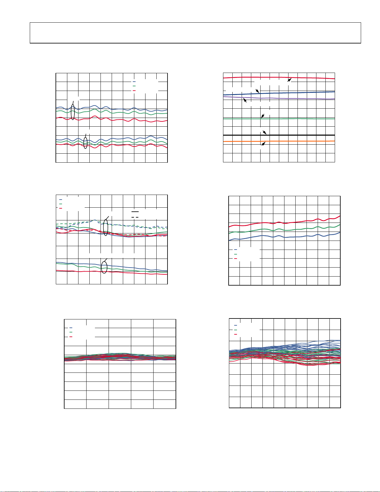
capabilities of the ADL5380 for low IF applications, such as
W-CDMA. The ADL5380 exhibits image rejection greater than
45 dB over a broad frequency range.
60
50
2.5MHz LOW IF
40
30
20
IMAGE REJECTI ON (dB)
10
0
400 800 1200 1600 2000 2400 2800 3200 3600 4000
5MHz LOW IF
7MHz LOW IF
RF FREQUENCY ( MHz)
07585-103
Figure 86. Low Band and Midband Image Rejection vs. RF Frequency for a
W-CDMA Signal, IF = 2.5 MHz, 5 MHz, and 7.5 MHz
60
50
40
2.5MHz LOW IF
30
20
IMAGE REJECTI ON (dB)
10
0
5000 5200 5400 5600 5800 6000
5MHz LOW IF
7MHz LOW IF
RF FREQ UENCY (MHz)
07585-104
Figure 87. High Band Image Rejection vs. RF Frequency for a W-CDMA Signal,
IF = 2.5 MHz, 5 MHz, and 7.5 MHz
EXAMPLE BASEBAND INTERFACE
In most direct-conversion receiver designs, it is desirable to
select a wanted carrier within a specified band. The desired
channel can be demodulated by tuning the LO to the appropriate
carrier frequency. If the desired RF band contains multiple
carriers of interest, the adjacent carriers are also down converted to
a lower IF frequency. These adjacent carriers can be problematic if
they are large relative to the wanted carrier because they can
overdrive the baseband signal detection circuitry. As a result, it
is often necessary to insert a filter to provide sufficient rejection
of the adjacent carriers.
It is necessary to consider the overall source and load impedance
presented by the ADL5380 and ADC input when designing the
filter network. The differential baseband output impedance of
the ADL5380 is 50 Ω. The ADL5380 is designed to drive a high
impedance ADC input. It may be desirable to terminate the
ADC input down to lower impedance by using a terminating
resistor, such as 500 Ω. The terminating resistor helps to better
define the input impedance at the ADC input at the cost of a
slightly reduced gain (see the Circuit Description section for
details on the emitter-follower output loading effects).
The order and type of filter network depends on the desired high
frequency rejection required, pass-band ripple, and group delay.
Filter design tables provide outlines for various filter types and
orders, illustrating the normalized inductor and capacitor values
for a 1 Hz cutoff frequency and 1 Ω load. After scaling the
normalized prototype element values by the actual desired
cut-off frequency and load impedance, the series reactance
elements are halved to realize the final balanced filter network
component values.
As an example, a second-order Butterworth, low-pass filter design
is shown in Figure 88 where the differential load impedance is
500 Ω and the source impedance of the ADL5380 is 50 Ω. The
normalized series inductor value for the 10-to-1, load-to-source
impedance ratio is 0.074 H, and the normalized shunt capacitor
is 14.814 F. For a 10.9 MHz cutoff frequency, the single-ended
equivalent circuit consists of a 0.54 µH series inductor followed
by a 433 pF shunt capacitor.
The balanced configuration is realized as the 0.54 µH inductor
is split in half to realize the network shown in Figure 88.
RS= 50
V
S
R
S
= 0.1
R
L
RS = 50Ω
V
S
R
S
= 25Ω
2
V
S
R
S
= 25Ω
2
Figure 88. Second-Order Butterworth, Low-Pass Filter Design Example
L
= 0.074H
N
NORMALIZE D
SINGLE-ENDED
CONFIGURAT ION
0.54µH
DENORMALIZED
SINGLE-ENDED
EQUIVALENT
0.27µH
BALANCED
CONFIGURAT ION
0.27µH
= 500Ω
14.814F
C
N
433pF
433pF
R
L
f
= 1Hz
C
= 500Ω
R
L
f
= 10.9MHz
C
R
L
= 250Ω
2
R
L
= 250Ω
2
7585-087
Rev. 0 | Page 26 of 36
Page 27

ADL5380
A complete design example is shown in Figure 91. A sixth-order
Butterworth differential filter having a 1.9 MHz corner frequency
interfaces the output of the ADL5380 to that of an ADC input.
The 500 Ω load resistor defines the input impedance of the
ADC. The filter adheres to typical direct conversion W-CDMA
applications where, 1.92 MHz away from the carrier IF frequency,
1 dB of rejection is desired, and, 2.7 MHz away from the carrier IF
frequency, 10 dB of rejection is desired.
Figure 89 and Figure 90 show the measured frequency response
and group delay of the filter.
10
5
0
–5
–10
MAGNITUDE RESPONSE (dB)
–15
–20
033.02.52.01.51.00.5
FREQUENCY (MHz)
.5
7585-088
Figure 89. Sixth-Order Baseband Filter Response
900
800
700
600
500
DELAY (ns)
400
300
200
100
0 0.2 0.4 0.6 0.8 1.0 1.2 1.4 1.6 1.8
FREQUENCY (MHz)
7585-089
Figure 90. Sixth-Order Baseband Filter Group Delay
Rev. 0 | Page 27 of 36
Page 28

ADL5380
V
V
S
0.1µF
S
0.1µF
100pF
100pF
RFIN
BALUN
100pF
24 23 22 21 20 19
ENBL
100pF
BALUN
RFIP
GND3
ADL5380
GND4
LOIP
VCC3
1
GND3
GND1
2
IHI
3
ILO
4
GND1
5
VCC1
6
7 8 9 10 11 12
RFIN
LOIN
100pF
100pF
GND3
GND4
ADJ
GND3
GND2
QHI
QLO
GND2
VCC2
NC
V
S
18
17
16
15
14
0.1µF
V
S
13
100pF
LO_SE
C
10µF
27µH
27µH
10µH
C
AC
270pF
100pF
68pF
500Ω
AC
10µF
27µH
27µH
10µH
C
AC
10µF
27µH
27µH
10µH
C
AC
10µF
270pF
100pF
68pF
500Ω
ADC INPUTADC INPUT
27µH
27µH
10µH
07585-090
Figure 91. Sixth-Order Low-Pass Butterworth, Baseband Filter Schematic
Rev. 0 | Page 28 of 36
Page 29

ADL5380
Ω
As the load impedance of the filter increases, the filter design
becomes more challenging in terms of meeting the required
rejection and pass band specifications. In the previous W-CDMA
example, the 500 Ω load impedance resulted in the design of a
sixth-order filter that has relatively large inductor values and small
capacitor values. If the load impedance is 200 Ω, the filter design
becomes much more manageable. Figure 92 shows a fourth-order
filter designed for a 10 MHz wide LTE signal. As shown in Figure 92,
the resultant inductor and capacitor values become much more
practical with a 200 Ω load.
2.2µH
1.5µH
50
2.2µH
22pF
100pF
1.5µH
200Ω
07585-091
Figure 92. Fourth-Order Low-Pass LTE Filter Schematic
Figure 93 and Figure 94 illustrate the magnitude response and
group delay response of the fourth-order filter, respectively.
5
0
–5
–10
–15
–20
–25
–30
FREQUENCY RESPO NSE (dB)
–35
–40
FREQUENCY (MHz)
4035302520151050
Figure 93. Fourth-Order Low-Pass LTE Filter Magnitude Response
6
0
5
0
4
0
3
0
2
0
GROUP DELAY (ns)
1
0
0
5 101520253035400
FREQUENCY (MHz)
07585-093
Figure 94. Fourth-Order Low-Pass LTE Filter Group Delay Response
07585-092
Rev. 0 | Page 29 of 36
Page 30

ADL5380
CHARACTERIZATION SETUPS
Figure 95 to Figure 97 show the general characterization bench
setups used extensively for the ADL5380. The setup shown in
Figure 97 was used to do the bulk of the testing and used sinusoidal
signals on both the LO and RF inputs. An automated Agilent
VEE program was used to control the equipment over the
IEEE bus. This setup was used to measure gain, IP1dB, IIP2,
IIP3, I/Q gain match, and quadrature error. The ADL5380
characterization board had a 9-to-1 impedance transformer on
each of the differential baseband ports to do the differential-tosingle-ended conversion, which presented a 450 Ω differential load
to each baseband port, when interfaced with 50 Ω test equipment.
For all measurements of the ADL5380, the loss of the RF input
balun was de-embedded. Due to the wideband nature of the
ADL5380, three different board configurations had to be used to
characterize the product. For low band characterization (400 MHz
to 3 GHz), the Mini-Circuits TC1-1-13 balun was used on the
RF and LO inputs to create differential signals at the device pins.
For midband characterization (3 GHz to 4 GHz), the Johanson
Technology 3600BL14M050T was used, and for high band
characterization (5 GHz to 6 GHz), the Johanson Technology
5400BL15B050E balun was used.
SNS
CONTROL
OUTPUT
The two setups shown in Figure 95 and Figure 96 were used
for making NF measurements. Figure 95 shows the setup for
measuring NF with no blocker signal applied while Figure 96
was used to measure NF in the presence of a blocker. For both
setups, the noise was measured at a baseband frequency of
10 MHz. For the case where a blocker was applied, the output
blocker was at a 15 MHz baseband frequency. Note that great
care must be taken when measuring NF in the presence of a
blocker. The RF blocker generator must be filtered to prevent
its noise (which increases with increasing generator output power)
from swamping the noise contribution of the ADL5380. At least
30 dB of attention at the RF and image frequencies is desired.
For example, assume a 915 MHz signal applied to the LO inputs of
the ADL5380. To obtain a 15 MHz output blocker signal, the RF
blocker generator is set to 930 MHz and the filters tuned such
that there is at least 30 dB of attenuation from the generator at
both the desired RF frequency (925 MHz) and the image RF
frequency (905 MHz). Finally, the blocker must be removed
from the output (by the 10 MHz low-pass filter) to prevent
the blocker from swamping the analyzer.
AGILENT N8974A
NOISE FI GURE ANALYZER
Q
I
IEEE
R1
50Ω
FROM SNS PORT
LOW-PASS
FILTER
INPUT
PC CONTROLLER
IEEE
07585-095
HP 6235A
POWER SUPPLY
AGILENT 8665B
SIGNAL G ENERATOR
RF
GND
ADL5380
CHAR BOARD
V
POS
LO
6dB PAD
Figure 95. General Noise Figure Measurement Setup
Rev. 0 | Page 30 of 36
Page 31

ADL5380
R&S SMT03
SIGNAL G ENERATOR
HP 6235A
POWER SUPPLY
AGILENT 8665B
SIGNAL G ENERATOR
BAND-PASS
TUNABLE FIL TER
6dB PAD
RF
GND
ADL5380
CHAR BOARD
V
POS
LO
6dB PAD
BAND-PASS
CAVITY FILTER
BAND-REJECT
TUNABLE FILTER
Q
50Ω
6dB PAD
I
R1
LOW-PASS
FILTER
HP 87405
LOW NOISE
PREAMP
R&S FSEA30
SPECTRUM ANALYZ ER
07585-096
Figure 96. Measurement Setup for Noise Figure in the Presence of a Blocker
3dB PAD
RF
R&S SMT06
RF
3dB PAD
3dB PAD
AGILENT
11636A
AMPLIFIER
VP GND
OUTIN
3dB PAD
RF
IEEE IEEE IEEE IEEE
R&S SMT06
AGILENT E3631
POWER SUPPLY
AGILENT E8257D
SIGNAL G ENERATOR
PC CONTROLLER
IEEE
GND
V
POS
6dB PAD
RF
ADL5380
CHAR BOARD
LO
6dB PAD
R&S FSEA30
SPECTRUM ANALYZ ER
Q
I
6dB PAD
6dB PAD
IEEE
RF
INPUT
VECTOR VOLTMETER
SWITCH
MATRIX
HP 8508A
IEEE
A AND B
INPUT CHANNELS
07585-097
Figure 97. General Characterization Setup
Rev. 0 | Page 31 of 36
Page 32

ADL5380
R
EVALUATION BOARD
The ADL5380 evaluation board is available. There are two
versions of the board, optimized for performance for separate
frequency ranges. For operation <3 GHz, an FR4 material-based
board with the TC1-1-13 balun footprint is available. For operation
between 3 GHz to 6 GHz, a Rogers® material-based RO3003 board
with the Johanson Technology 3600BL14M050 balun (optimal
for operation between 3 GHz and 4 GHz) footprint is available.
RFx
C5x C12x
The Johanson Technology 5400BL15K050 shares the same
footprint and can be used for operation between 4900 MHz to
5800 MHz.
The board can be used for single-ended or differential baseband
analysis. The default configuration of the board is for single-ended
baseband analysis.
T3x
R7x
R10x
R19x
C6x
R11x
V
POS
C8x
24 23 22 21 20 19
VCC3
GND3
1
GND3
2
GND1
3
IHI
4
ILO
5
GND1
6
VCC1
ENBL
GND4
789101112
R1xR9x
V
POS
C1x
P1x
LOPx
RFIP
RFIN
ADL5380
LOIP
LOIN
T1x
LO_SE
C3xC2x
V
POS
C11x
R17x
T4x
R5x
R4x
V
R16x
C16x
R15x
POS
C9x
IPx
INx
NOTES
1. X = B, FOR LOW FREQUENCY OPERATION UP T O 3GHz, TC1-1-13 BALUN ON RF AND LO PO RTS.
X = A, FOR FREQUENCY OPERATION F ROM 3GHz T O 4GHz, JOHANSON TECHNO LOGY 3600BL 14M050 BALUN ON RF AND L O PORTS.
2. FOR OP ERATION BE TWEEN 4. 9GHZ TO 6GHZ, T HE JOHANSON T ECHNOLOG Y 5400BL15K050 BALUN, WHICH SHARES A SIMILA
FOOTPRINT AS THE 4GHZ BALUN, CAN BE USED.
GND3
GND4
LONx
C4x
ADJ
NC
R23x
GND3
GND2
QHI
QLO
GND2
VCC2
V
POS
18
R14x
C15x
R13x
C10x
R3x
T2x
R2x
V
POS
R18x
QPx
QNx
07585-098
17
16
15
14
13
R6x
R12x
C7x
Figure 98. Evaluation Board Schematic
Rev. 0 | Page 32 of 36
Page 33

ADL5380
Table 5. Evaluation Board Configuration Options
Component Description Default Condition
VPOSx, GNDx Power Supply and Ground Vector Pins. Not applicable
R10x, R12x,
R19x
C6x to C11x The capacitors provide the required dc coupling up to 6 GHz.
P1x, R11x,
R9x, R1x
R23x
C1x to C5x,
C12x
R2x to R7x,
R13x to R18x
T2x, T4x
C15x, C16x
T1x
T3x
Power Supply Decoupling. Shorts or power supply decoupling resistors. R10x, R12x, R19x = 0 Ω (0603)
C6x, C7x, C8x = 100 pF (0402),
C9x, C10x, C11x = 0.1 μF (0603)
Device Enable. When connected to V
, the device is active.
S
P1x, R9x = DNI, R1x = DNI,
R11x = 0 Ω
Adjust Pin. The resistor value here sets the bias voltage at this pin and optimizes
third-order distortion.
AC Coupling Capacitors. These capacitors provide the required ac coupling
from 400 MHz to 4 GHz.
Single-Ended Baseband Output Path. This is the default configuration of the
evaluation board. R13x to R18x are populated for appropriate balun interface.
R23B = 1.5 kΩ (0603),
R23A = 200 Ω (0603)
C1x, C4x = DNI,
C2x, C3x, C5x, C12x = 100 pF (0402)
R2x to R7x = open,
R13x to R18x = 0 Ω (0402)
R2x to R5x are not populated. Baseband outputs are taken from QHI and IHI. The
user can reconfigure the board to use full differential baseband outputs. R2x to R5x
provide a means to bypass the 9:1 TCM9-1 transformer to allow for differential baseband outputs. Access the differential baseband signals by populating R2x to R5x
with 0 Ω and not populating R13x to R18x. This way the transformer does not need
to be removed. The baseband outputs are taken from the SMAs of QHI, QLO, IHI,
and ILO. R6x and R7x are provisions for applying a specific differential load across
the baseband outputs
IF Output Interface. TCM9-1 converts a differential high impedance IF output to
T2x, T4x = TCM9-1, 9:1 (Mini-Circuits)
a single-ended output. When loaded with 50 Ω, this balun presents a 450 Ω load
to the device. The center tap can be decoupled through a capacitor to ground.
Decoupling Capacitors. C15x and C16x are the decoupling capacitors used to reject
C15x, C16x = 0.1 μF (0402)
noise on the center tap of the TCM9-1.
LO Input Interface. A 1:1 RF balun that converts the single-ended RF input to
differential signal is used.
T1B = TC1-1-13, 1:1 (Mini-Circuits)
for operation <3 GHz,
T1A = Johanson Technology
3600BL14M050 for operation from
3 GHz to 4 GHz, Johanson Technology
5400BL15K050 for operation from
4900 MHz to 5800 MHz
RF Input Interface. A 1:1 RF balun that converts the single-ended RF input to
differential signal is used.
T3B = TC1-1-13, 1:1 (Mini-Circuits)
for operation <3 GHz,
T3A = Johanson Technology
3600BL14M050 for operation from
3 GHz to 4 GHz, Johanson Technology
5400BL15K050 for operation from
4900 MHz to 5800 MHz
Rev. 0 | Page 33 of 36
Page 34

ADL5380
Figure 99. Low Band Evaluation Board Top Layer
7585-100
Figure 100. Midband/High Band Evaluation Board Top Layer Silkscreen
THERMAL GROUNDING AND EVALUATION BOARD LAYOUT
The package for the ADL5380 features an exposed paddle on the
underside that should be well soldered to a low thermal and
electrical impedance ground plane. This paddle is typically
soldered to an exposed opening in the solder mask on the
evaluation board. Figure 103 illustrates the dimensions used in
the layout of the ADL5380 footprint on the ADL5380 evaluation
board (1 mil = 0.0254 mm).
Notice the use of nine via holes on the exposed paddle. These
ground vias should be connected to all other ground layers on
the evaluation board to maximize heat dissipation from the
device package.
Rev. 0 | Page 34 of 36
07585-099
7585-101
Figure 101. Low Band Evaluation Board Bottom Layer
7585-102
Figure 102. Midband/High Band Evaluation Board Bottom Layer Silkscreen
12 mil.
25 mil.
12 mil.
19.7 mil.
98.4 mil.
133.8 mil.
23 mil.
82 mil.
07585-105
Figu re 103 . Dimen sions for Evaluation Board Layout for the ADL5380 Package
Under these conditions, the thermal impedance of the ADL5380
was measured to be approximately 30°C/W in still air.
Page 35

ADL5380
OUTLINE DIMENSIONS
4.00
PIN 1
INDICATOR
1.00
0.85
0.80
SEATING
PLANE
12° MAX
BSC SQ
TOP
VIEW
0.80 MAX
0.65 TYP
COMPLIANT TO JEDEC S TANDARDS MO-220-V GGD-8
0.30
0.23
0.18
3.75
BSC SQ
0.20 REF
0.05 MAX
0.02 NOM
COPLANARITY
0.60 MAX
0.50
BSC
0.50
0.40
0.30
0.08
2.50 REF
Figure 104. 24-Lead Lead Frame Chip Scale Package [LFCSP_VQ]
4 mm × 4 mm Body, Very Thin Quad
(CP-24-3)
Dimensions shown in millimeters
0.60 MAX
PIN 1
INDICATOR
1
24
19
18
EXPOSED
PA D
(BOTTOMVIEW)
13
12
6
7
FOR PRO PER CONNECTIO N OF
THE EXPOSED PAD, REFER TO
THE PIN CONF IGURATIO N AND
FUNCTION DES CRIPTIONS
SECTION O F THIS DAT A SHEET.
2.65
2.50 SQ
2.35
0.23 MIN
082908-A
ORDERING GUIDE
Package
Model Temperature Range Package Description
ADL5380ACPZ-R71 –40°C to +85°C 24-Lead LFCSP_VQ CP-24-3 1,500, 7” Tape and Reel
ADL5380ACPZ-WP1 –40°C to +85°C 24-Lead LFCSP_VQ CP-24-3 64, Waffle Pack
ADL5380-29A-EVALZ1 Mid Band (3 GHz to 4 GHz) Evaluation Board 1
ADL5380-30A-EVALZ1 Low Band (400 MHz to 3 GHz) Evaluation Board 1
1
Z = RoHS Compliant Part.
Option
Ordering Quantity
Rev. 0 | Page 35 of 36
Page 36

ADL5380
NOTES
©2009 Analog Devices, Inc. All rights reserved. Trademarks and
registered trademarks are the property of their respective owners.
D07585-0-7/09(0)
Rev. 0 | Page 36 of 36
 Loading...