

Page 1
LF to 4 GHz
R
FEATURES
Broadband radio frequency (RF), intermediate frequency (IF),
and local oscillator (LO) ports
Conversion loss: 6.8 dB
Noise figure: 6.5 dB
High input IP3: 25 dBm
High input P1dB: 19 dBm
Low LO drive level
Single-ended design: no need for baluns
Single-supply operation: 3 V @ 19 mA
Miniature, 2 mm × 3 mm, 8-lead LFCSP
RoHS compliant
APPLICATIONS
Cellular base stations
Point-to-point radio links
RF instrumentation
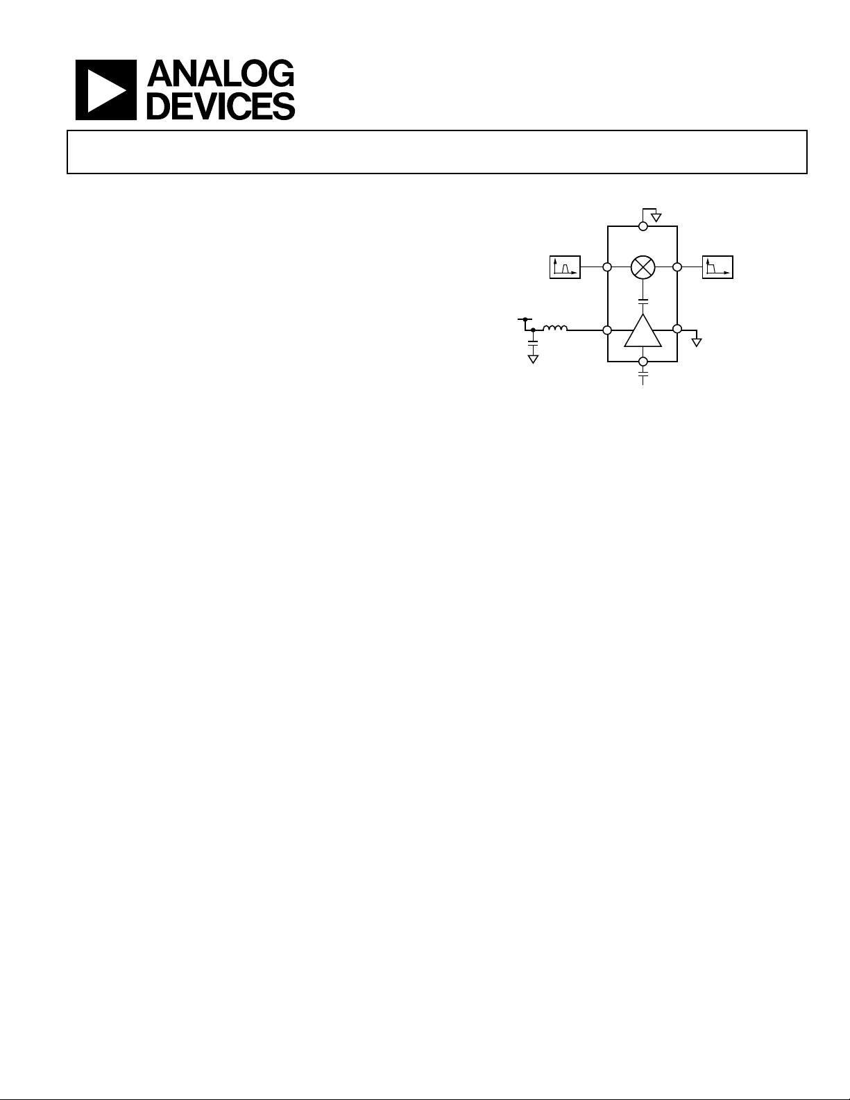
High Linearity Y-Mixer
ADL5350
FUNCTIONAL BLOCK DIAGRAM
GND
ADL5350
RF IF
LO
LO
INPUT
Figure 1.
3V
RF
INPUT OR
OUTPUT
VPOS
OUTPUT O
INPUT
GND
IF
05615-001
GENERAL DESCRIPTION
The ADL5350 is a high linearity, up-and-down converting
mixer capable of operating over a broad input frequency range.
It is well suited for demanding cellular base station mixer designs
that require high sensitivity and effective blocker immunity. Based
on a GaAs pHEMT, single-ended mixer architecture, the ADL5350
provides excellent input linearity and low noise figure without
the need for a high power level LO drive.
In 850 MHz/900 MHz receive applications, the ADL5350
provides a typical conversion loss of only 6.7 dB. The input IP3
is typically greater than 25 dBm, with an input compression
point of 19 dBm. The integrated LO amplifier allows a low LO
drive level, typically only 4 dBm for most applications.
The high input linearity of the ADL5350 makes the device an
excellent mixer for communications systems that require high
blocker immunity, such as GSM 850 MHz/900 MHz and
800 MHz CDMA2000. At 2 GHz, a slightly greater supply
current is required to obtain similar performance.
The single-ended broadband RF/IF port allows the device to be
customized for a desired band of operation using simple external
filter networks. The LO-to-RF isolation is based on the LO
rejection of the RF port filter network. Greater isolation can be
achieved by using higher order filter networks, as described in
the
Applications Information section.
The ADL5350 is fabricated on a GaAs pHEMT, high performance
IC process. The ADL5350 is available in a 2 mm × 3 mm, 8-lead
LFCSP. It operates over a −40°C to +85°C temperature range.
An evaluation board is also available.
Rev. 0
Information furnished by Analog Devices is believed to be accurate and reliable. However, no
responsibility is assumed by Anal og Devices for its use, nor for any infringements of patents or ot her
rights of third parties that may result from its use. Specifications subject to change without notice. No
license is granted by implication or otherwise under any patent or patent rights of Analog Devices.
Trademarks and registered trademarks are the property of their respective owners.
One Technology Way, P.O. Box 9106, Norwood, MA 02062-9106, U.S.A.
Tel: 781.329.4700 www.analog.com
Fax: 781.461.3113 ©2008 Analog Devices, Inc. All rights reserved.
Page 2

ADL5350
TABLE OF CONTENTS
Features .............................................................................................. 1
Applications....................................................................................... 1
Functional Block Diagram .............................................................. 1
General Description......................................................................... 1
Revision History ............................................................................... 2
Specifications..................................................................................... 3
850 MHz Receive Performance .................................................. 3
1950 MHz Receive Performance ................................................ 3
Spur Tables......................................................................................... 4
850 MHz Spur Table..................................................................... 4
1950 MHz Spur Table................................................................... 4
Absolute Maximum Ratings............................................................ 5
ESD Caution.................................................................................. 5
Pin Configuration and Function Descriptions............................. 6
Typical Perf or m an c e Charac t e r istics ..............................................7
850 MHz Characteristics..............................................................7
1950 MHz Characteristics......................................................... 12
Functional Description .................................................................. 17
Circuit Description .................................................................... 17
Implementation Procedure....................................................... 17
Applications Information.............................................................. 19
Low Frequency Applications .................................................... 19
High Frequency Applications................................................... 19
Evaluation Board ............................................................................ 21
Outline Dimensions ....................................................................... 22
Ordering Guide .......................................................................... 22
REVISION HISTORY
2/08—Revision 0: Initial Version
Rev. 0 | Page 2 of 24
Page 3

ADL5350
SPECIFICATIONS
850 MHz RECEIVE PERFORMANCE
VS = 3 V, TA = 25°C, LO power = 4 dBm, re: 50 Ω, unless otherwise noted.
Table 1.
Parameter Min Typ Max Unit Conditions
RF Frequency Range 750 850 975 MHz
LO Frequency Range 500 780 945 MHz Low-side LO
IF Frequency Range 30 70 250 MHz
Conversion Loss 6.7 dB fRF = 850 MHz, fLO = 780 MHz, fIF = 70 MHz
SSB Noise Figure 6.4 dB fRF = 850 MHz, fLO = 780 MHz, fIF = 70 MHz
Input Third-Order Intercept (IP3) 25 dBm
Input 1dB Compression Point (P1dB) 19.8 dBm fRF = 820 MHz, fLO = 750 MHz, fIF = 70 MHz
LO-to-IF Leakage 29 dBc LO power = 4 dBm, fLO = 780 MHz
LO-to-RF Leakage 13 dBc LO power = 4 dBm, fLO = 780 MHz
RF-to-IF Leakage 19.5 dBc RF power = 0 dBm, fRF = 850 MHz, fLO = 780 MHz
IF/2 Spurious −50 dBc RF power = 0 dBm, fRF = 850 MHz, fLO = 780 MHz
Supply Voltage 2.7 3 3.5 V
Supply Current 16.5 mA LO power = 4 dBm
= 849 MHz, f
f
RF1
each RF tone 0 dBm
= 850 MHz, fLO = 780 MHz, fIF = 70 MHz;
RF2
1950 MHz RECEIVE PERFORMANCE
VS = 3 V, TA = 25°C, LO power = 6 dBm, re: 50 Ω, unless otherwise noted.
Table 2.
Parameter Min Typ Max Unit Conditions
RF Frequency Range 1800 1950 2050 MHz
LO Frequency Range 1420 1760 2000 MHz Low-side LO
IF Frequency Range 50 190 380 MHz
Conversion Loss 6.8 dB fRF = 1950 MHz, fLO = 1760 MHz, fIF = 190 MHz
SSB Noise Figure 6.5 dB fRF = 1950 MHz, fLO = 1760 MHz, fIF = 190 MHz
Input Third-Order Intercept (IP3) 25 dBm
Input 1dB Compression Point (P1dB) 19 dBm fRF = 1950 MHz, fLO = 1760 MHz, fIF = 190 MHz
LO-to-IF Leakage 13.5 dBc LO power = 6 dBm, fLO = 1760 MHz
LO-to-RF Leakage 10.5 dBc LO power = 6 dBm, fLO = 1760 MHz
RF-to-IF Leakage 11.5 dBc RF power = 0 dBm, fRF = 1950 MHz, fLO = 1760 MHz
IF/2 Spurious −54 dBc RF power = 0 dBm, fRF = 1950 MHz, fLO = 1760 MHz
Supply Voltage 2.7 3 3.5 V
Supply Current 19 mA LO power = 6 dBm
= 1949 MHz, f
f
RF1
each RF tone 0 dBm
RF2
= 1951 MHz, fLO = 1760 MHz, fIF = 190 MHz;
Rev. 0 | Page 3 of 24
Page 4

ADL5350
SPUR TABLES
All spur tables are (N × fRF) − (M × fLO) mixer spurious products for 0 dBm input power, unless otherwise noted. N.M. indicates that a
spur was not measured due to it being at a frequency >6 GHz.
850 MHz SPUR TABLE
Table 3.
0 1 2 3 4 5 6 7 8 9 10 11 12 13 14 15
0 ≤–100 –20.6 –19.2 –15.3 –16.7 –38.4 –26.6 –22.1 N.M. N.M. N.M. N.M. N.M. N.M. N.M. N.M .
1 –21.6 –5.6 –23. 6 –19. 6 –31.9 –28.7 –46.1 –48.5 –33. 2 N. M. N.M. N. M. N.M. N.M. N. M. N.M.
2 –50.0 –69.2 –50.5 –59.8 –49. 1 –57.5 –51.0 –77.7 –65.8 –60. 8 N.M. N.M. N. M. N.M. N.M. N.M.
3 –74.8 –66.0 –71.8 –68.1 –70. 2 –67.4 –66.9 –70.8 –85.2 –87. 3 –72.2 N. M. N.M. N.M. N.M . N.M.
4 ≤–100 –92.6 –91.6 –96.1 –92.7 –98.7 –90.2 –91.7 –88.8 ≤–100 ≤–100 –91.7 –88.6 N.M. N.M. N.M.
5 ≤–100 ≤–100 ≤–100 ≤–100 ≤–100 ≤–100 ≤–100 ≤–100 –99.5 ≤–100 ≤–100 ≤–100 ≤–100 ≤–100 N.M. N .M.
6 ≤–100 ≤–100 ≤–100 ≤–100 ≤–100 ≤–100 ≤–100 ≤–100 ≤–100 ≤–100 ≤–100 ≤–100 ≤–100 ≤–100 ≤–100 N.M.
N
7 ≤–100 ≤–100 ≤–100 ≤–100 ≤–100 ≤–100 ≤–100 ≤–100 ≤–100 ≤–100 ≤–100 ≤–100 ≤–100 ≤–100 ≤–100 ≤–100
8 N.M. N.M. ≤–100 ≤–100 ≤–100 ≤–100 ≤–100 ≤–100 ≤–100 ≤–100 ≤–100 ≤–100 ≤–100 ≤–100 ≤–100 ≤–100
9 N.M. N.M. N.M. ≤–100 ≤–100 ≤–100 ≤–100 ≤–100 ≤–100 ≤–100 ≤–100 ≤–100 ≤–100 ≤–100 ≤–100 ≤–100
10 N.M. N.M. N.M. N.M. ≤–100 ≤–100 ≤–100 ≤–100 ≤–100 ≤–100 ≤–100 ≤–100 ≤–100 ≤–100 ≤–100 ≤–100
11 N.M. N.M. N.M. N.M. N.M. ≤–100 ≤–100 ≤–100 ≤–100 ≤–100 ≤–100 ≤–100 ≤–100 ≤–100 ≤–100 ≤–100
12 N.M. N.M. N.M. N.M. N.M. N. M. ≤–100 ≤–100 ≤–100 ≤–100 ≤–100 ≤–100 ≤–100 ≤–100 ≤–100 ≤–100
13 N.M. N.M. N.M. N.M. N.M. N. M. N.M. ≤–100 ≤–100 ≤–100 ≤–100 ≤–100 ≤–100 ≤–100 ≤–100 ≤–100
14 N.M. N.M. N.M. N.M. N.M. N.M. N.M. N.M. ≤–100 ≤–100 ≤–100 ≤–100 ≤–100 ≤–100 ≤–100 ≤–100
15 N.M. N.M. N.M. N.M. N.M. N.M. N.M. N.M. N.M. ≤–100 ≤–100 ≤–100 ≤–100 ≤–100 ≤–100 ≤–100
1950 MHz SPUR TABLE
M
05615–068
Table 4.
0 ≤–100 –13.1 –32.8 –22.4 N.M. N.M. N. M. N.M . N.M. N.M. N.M. N.M . N.M. N.M. N.M. N. M.
1 –10. 8 –7. 0 –25.3 – 27.7 –33. 9 N.M. N.M. N.M. N.M. N.M. N.M . N.M. N. M. N.M. N. M. N. M.
2 –48. 2 –61. 2 –41. 2 –44.6 –47.0 –74.6 N.M. N.M. N.M. N.M. N. M. N.M . N.M. N.M. N.M. N. M.
3 –72. 3 –71. 4 –83. 6 –64.5 –62.4 –64.3 –83.7 N.M. N. M. N.M. N.M . N.M. N. M. N.M. N. M. N. M.
4 N. M. N.M. –91. 4 –84.2 –78.3 –76.5 –80.0 –92.0 N.M. N. M. N.M. N.M. N.M. N. M. N.M. N.M.
5 N. M. N.M. N.M . –90.8 –82.3 –77.1 –79.5 –83.8 –95.2 N. M. N.M. N.M. N.M. N.M. N.M. N.M.
6 N.M.N.M.N.M.N.M.≤–100 ≤–100 –93.4 –94.5 ≤–100 –99.2 ≤–100 N.M. N.M. N.M. N. M. N.M.
N
7 N.M.N.M.N.M.N.M.N.M.≤–100 ≤–100 –94.0 –96.4 ≤–100 ≤–100 ≤–100 N.M. N. M. N.M. N.M.
8 N.M.N.M.N.M.N.M.N.M.N.M.≤–100 ≤–100 ≤–100 ≤–100 ≤–100 ≤–100 ≤–100 N.M . N.M. N.M.
9 N.M.N.M.N.M.N.M.N.M.N.M.N.M.≤–100 ≤–100 ≤–100 ≤–100 ≤–100 ≤–100 ≤–100 N .M. N. M.
10 N.M. N.M. N.M. N.M. N.M. N.M. N.M. N.M. ≤–100 ≤–100 ≤–100 ≤–100 ≤–100 ≤–100 ≤–100 N.M.
11 N.M. N.M. N.M. N.M. N.M. N.M. N.M. N.M. N.M. ≤–100 ≤–100 ≤–100 ≤–100 ≤–100 ≤–100 ≤–100
12 N.M. N.M. N.M. N.M. N.M. N.M. N.M. N.M. N.M. N.M. ≤–100 ≤–100 ≤–100 ≤–100 ≤–100 ≤–100
13 N.M. N.M. N.M. N.M. N.M. N.M. N.M. N.M. N.M. N.M. N.M. ≤–100 ≤–100 ≤–100 ≤–100 ≤–100
14 N.M. N.M. N.M. N.M. N.M. N.M. N.M. N.M. N.M. N.M. N.M. N.M. N.M. ≤–100 ≤–100 ≤–100
15 N.M. N.M. N.M. N.M. N.M. N.M. N.M. N.M. N.M. N.M. N.M. N.M. N.M. N.M. ≤–100 ≤–100
0123456789101112131415
M
05615–069
Rev. 0 | Page 4 of 24
Page 5
ADL5350
ABSOLUTE MAXIMUM RATINGS
Table 5.
Parameter Rating
Supply Voltage, VS 4.0 V
RF Input Level 23 dBm
LO Input Level 20 dBm
Internal Power Dissipation 324 mW
θJA 154.3°C/W
Maximum Junction Temperature 135°C
Operating Temperature Range −40°C to +85°C
Storage Temperature Range −65°C to +150°C
Stresses above those listed under Absolute Maximum Ratings
may cause permanent damage to the device. This is a stress
rating only; functional operation of the device at these or any
other conditions above those indicated in the operational
section of this specification is not implied. Exposure to absolute
maximum rating conditions for extended periods may affect
device reliability.
ESD CAUTION
Rev. 0 | Page 5 of 24
Page 6

ADL5350
PIN CONFIGURATION AND FUNCTION DESCRIPTIONS
1RF/IF
2GND2
ADL5350
TOP VIEW
3LOIN
(Not to Scale)
4NC
NC = NO CONNECT
Figure 2. Pin Configuration
8 RF/IF
7NC
6 VPOS
5 GND1
05615-002
Table 6. Pin Function Descriptions
Pin No. Mnemonic Description
1, 8 RF/IF
RF and IF Input/Output Ports. These nodes are internally tied together. RF and IF port separation is
achieved using external tuning networks.
2, 5, Paddle GND2, GND1, GND Device Common (DC Ground).
3 LOIN LO Input. Needs to be ac-coupled.
4, 7 NC No Connect. Grounding NC pins is recommended.
6 VPOS
Positive Supply Voltage for the Drain of the LO Buffer. A series RF choke is needed on the supply line
to provide proper ac loading of the LO buffer amplifier.
Rev. 0 | Page 6 of 24
Page 7
ADL5350
TYPICAL PERFORMANCE CHARACTERISTICS
850 MHz CHARACTERISTICS
Supply voltage = 3 V, RF frequency = 850 MHz, IF frequency = 70 MHz, RF level = 0 dBm, LO level = 4 dBm, TA = 25°C, unless otherwise noted.
20
19
18
17
16
15
14
13
SUPPLY CURRENT (mA)
12
11
10
–40–200 20406080
TEMPERATURE ( °C)
Figure 3. Supply Current vs. Temperature
10
9
8
7
6
5
4
3
CONVERSION LOSS (dB)
2
1
0
–40 806040200–20
TEMPERATURE ( °C)
Figure 4. Conversion Loss vs. Temperature
28
27
26
25
24
23
22
INPUT IP3 (dBm)
21
20
19
18
–40 806040200–20
TEMPERATURE ( °C)
Figure 5. Input IP3 (IIP3) vs. Temperature
05615-003
05615-004
05615-005
INPUT P1dB (dBm)
22
20
18
16
14
SUPPLY CURRENT (mA)
12
10
7.4
7.2
7.0
6.8
6.6
6.4
CONVERSION LOSS (dB)
6.2
6.0
23
22
21
20
19
18
17
16
15
14
13
–40 806040200–20
TEMPERATURE ( °C)
Figure 6. Input P1dB vs. Temperature
+25°C
–40°C +85°C
2.7 3.53.43.33.23.13.02.92.8
SUPPLY VOLTAGE (V)
Figure 7. Supply Current vs. Supply Voltage
2.7 3.53.43.33.23.13.02.92.8
SUPPLY VOLTAGE (V)
Figure 8. Conversion Loss vs. Supply Voltage
+85°C
+25°C
–40°C
05615-006
05615-007
05615-008
Rev. 0 | Page 7 of 24
Page 8
ADL5350
Supply voltage = 3 V, RF frequency = 850 MHz, IF frequency = 70 MHz, RF level = 0 dBm, LO level = 4 dBm, TA = 25°C, unless otherwise noted.
28
22
INPUT IP3 (dBm)
INPUT P1dB (dBm)
27
26
25
24
23
22
2.7 3.53.43.33.23.13.02.92.8
23
22
21
20
19
18
17
+85°C
SUPPLY VOLTAGE (V)
Figure 9. Input IP3 vs. Supply Voltage
–40°C
+25°C
+85°C
–40°C
+25°C
20
18
16
14
SUPPLY CURRENT (mA)
12
10
750 975950925900875850825800775
05615-009
–40°C
+25°C
RF FREQUENCY ( MHz)
+85°C
05615-012
Figure 12. Supply Current vs. RF Frequency
7.6
7.4
7.2
7.0
6.8
6.6
6.4
CONVERSION LOSS (dB)
6.2
6.0
+85°C
+25°C
–40°C
NOISE FI GURE (dB)
16
2.7 3.53.43.33.23.13.02.92.8
SUPPLY VOLTAGE (V)
Figure 10. Input P1dB vs. Supply Voltage
8.0
7.5
7.0
6.5
6.0
5.5
5.0
2.7 3. 53.43.33.23.13.02.92.8
SUPPLY VOLTAGE (V)
Figure 11. Noise Figure vs. Supply Voltage
05615-010
05615-011
5.8
750 800 850 900 950
RF FREQUENCY (M Hz)
Figure 13. Conversion Loss vs. RF Frequency
27.0
26.5
INPUT IP3 (dBm)
26.0
25.5
25.0
24.5
24.0
23.5
23.0
22.5
22.0
750 975950925900875850825800775
+85°C
RF FREQUENCY (M Hz)
–40°C
+25°C
Figure 14. Input IP3 vs. RF Frequency
05615-013
05615-014
Rev. 0 | Page 8 of 24
Page 9

ADL5350
Supply voltage = 3 V, RF frequency = 850 MHz, IF frequency = 70 MHz, RF level = 0 dBm, LO level = 4 dBm, TA = 25°C, unless otherwise noted.
INPUT P1dB (dBm)
23
22
21
20
19
18
17
16
750 975950925900875850825800775
8
–40°C
+25°C
+85°C
RF FREQUENCY (M Hz)
Figure 15. Input P1dB vs. RF Frequency
05615-015
9
8
+25°C
7
6
5
4
3
CONVERSION LOSS (dB)
2
1
0
25 50 75 100 125 150 175 200 225 250
+85°C
–40°C
IF FREQUENCY (MHz)
Figure 18. Conversion Loss vs. IF Frequency
28
05615-018
7
6
5
4
3
NOISE FI GURE (dB)
2
1
0
750 775 800 825 850 875 900 925 950 975
RF FREQ UENCY ( MHz)
Figure 16. Noise Figure vs. RF Frequency
22
20
18
16
14
12
SUPPLY CURRENT (mA)
10
+25°C
+85°C
–40°C
27
–40°C
26
25
INPUT IP3 (dBm)
24
23
22
25 50 75 100 125 150 175 200 225 250
05615-016
+25°C
+85°C
IF FREQUENCY (MHz)
05615-019
Figure 19. Input IP3 vs. IF Frequency
23
22
21
20
19
INPUT P1dB (dBm)
18
17
–40°C
+25°C
+85°C
8
25 50 75 100 125 150 175 200 225 250
IF FREQUENCY (MHz)
Figure 17. Supply Current vs. IF Frequency
05615-017
16
25 50 75 100 125 150 175 200 225 250
IF FREQUENCY (MHz)
Figure 20. Input P1dB vs. IF Frequency
05615-020
Rev. 0 | Page 9 of 24
Page 10

ADL5350
Supply voltage = 3 V, RF frequency = 850 MHz, IF frequency = 70 MHz, RF level = 0 dBm, LO level = 4 dBm, TA = 25°C, unless otherwise noted.
NOISE FI GURE (dB)
SUPPLY CURRENT (mA)
10
9
8
7
6
5
4
3
2
1
0
50 350300250200150100
18
16
14
12
10
8
6
4
2
0
–6 121086420–2–4
20
IF FREQUENCY (MHz)
Figure 21. Noise Figure vs. IF Frequency
+85°C
–40°C
+25°C
LO LEVEL (dBm)
Figure 22. Supply Current vs. LO Level
05615-021
05615-022
INPUT IP3 (dBm)
INPUT P1dB (dBm)
27
25
23
21
19
17
15
13
–6 121086420–2–4
22
21
20
19
+85°C
18
17
16
15
–6 121086420–2–4
12
LO LEVEL (dBm)
Figure 24. Input IP3 vs. LO Level
–40°C
+25°C
LO LEVEL (dBm)
Figure 25. Input P1dB vs. LO Level
+25°C
–40°C
+85°C
05615-024
05615-025
NOISE FI GURE (dB)
11
10
9
8
7
6
5
4
–2 1086420
LO LEVEL (dBm)
Figure 26. Noise Figure vs. LO Level
05615-026
18
16
14
12
10
CONVERSION LOSS (dB)
8
6
–6 121086420–2–4
+85°C
–40°C
+25°C
LO LEVEL (dBm)
05615-023
Figure 23. Conversion Loss vs. LO Level
Rev. 0 | Page 10 of 24
Page 11

ADL5350
–
–
Supply voltage = 3 V, RF frequency = 850 MHz, IF frequency = 70 MHz, RF level = 0 dBm, LO level = 4 dBm, TA = 25°C, unless otherwise noted.
IF FEEDT HROUGH (dBc)
13
–14
–15
–16
–17
–18
–19
–20
–21
–40°C
+25°C
+85°C
750 975950925900875850825800775
RF FREQUENCY (M Hz)
Figure 27. IF Feedthrough vs. RF Frequency
15
–20
–25
–30
+25°C
+85°C
05615-027
0
–2
–4
–6
–8
–10
–12
RF LEAKAGE ( dBc)
–14
–16
–18
–20
630 680 730 780 830 880 930
LO FREQUENCY (MHz)
Figure 29. RF Leakage vs. LO Frequency
05615-029
–35
IF FEEDT HROUGH (dBc)
–40
–45
680 905880855830805780755730705
LO FREQUENCY (MHz)
–40°C
05615-028
Figure 28. IF Feedthrough vs. LO Frequency
Rev. 0 | Page 11 of 24
Page 12

ADL5350
1950 MHz CHARACTERISTICS
Supply voltage = 3 V, RF frequency = 1950 MHz, IF frequency = 190 MHz, RF level = −10 dBm, LO level = 6 dBm, TA = 25°C,
unless otherwise noted.
20
19
18
17
16
15
14
13
SUPPLY CURRENT (mA)
12
11
10
–40–200 20406080
TEMPERATURE ( °C)
Figure 30. Supply Current vs. Temperature
10
9
8
7
6
5
4
3
CONVERSION LOSS (dB)
2
1
0
–40–200 20406080
TEMPERATURE ( °C)
Figure 31. Conversion Loss vs. Temperature
28
27
26
25
24
23
22
INPUT IP3 (dBm)
21
20
19
18
–40 –20 0 20 40 60 80
TEMPERATURE (° C)
Figure 32. Input IP3 vs. Temperature
05615-030
05615-031
05615-032
23
22
21
20
19
18
17
INPUT P1dB (dBm)
16
15
14
13
–40–200 20406080
TEMPERATURE ( °C)
Figure 33. Input P1dB vs. Temperature
22
+25°C
+85°C
SUPPLY VOLTAGE (V)
SUPPLY CURRENT (mA)
20
18
16
14
12
10
2.7 3.53.43.33.23.13.02.92.8
–40°C
Figure 34. Supply Current vs. Supply Voltage
7.4
7.2
+85°C
+25°C
–40°C
CONVERSION LOSS (dB)
7.0
6.8
6.6
6.4
6.2
6.0
2.7 3.53.43.33.23.13.02.92.8
SUPPLY VOLTAGE (V)
Figure 35. Conversion Loss vs. Supply Voltage
05615-033
05615-034
05615-035
Rev. 0 | Page 12 of 24
Page 13

ADL5350
Supply voltage = 3 V, RF frequency = 1950 MHz, IF frequency = 190 MHz, RF level = −10 dBm, LO level = 6 dBm, TA = 25°C,
unless otherwise noted.
28
27
26
25
INPUT IP3 (dBm)
24
23
+85°C
+25°C
–40°C
22
+25°C
20
18
16
14
SUPPLY CURRENT (mA)
12
+85°C
–40°C
INPUT P1dB (dBm)
NOISE FI GURE (dB)
22
2.7 3.53.43.33.23.13.02.92.8
SUPPLY VOLTAGE (V)
Figure 36. Input IP3 vs. Supply Voltage
20
19
18
17
16
2.7 3.53.43.33.23.13.02.92.8
SUPPLY VOLTAGE (V)
Figure 37. Input P1dB vs. Supply Voltage
8.0
7.5
7.0
6.5
6.0
5.5
5.0
2.7 3.53.43.33.23.13.02.92.8
SUPPLY VOLTAGE (V)
Figure 38. Noise Figure vs. Supply Voltage
+85°C
+25°C
–40°C
10
1800 1825 1850 1875 1900 1925 1950 1975 2000 2025 2050
05615-036
RF FREQUENCY (MHz)
05615-039
Figure 39. Supply Current vs. RF Frequency
7.6
7.4
7.2
7.0
6.8
6.6
6.4
CONVERSION LOSS (dB)
6.2
6.0
5.8
1800 2050202520001975195019251900187518501825
05615-037
RF FREQ UENCY ( MHz)
+85°C
+25°C
–40°C
05615-040
Figure 40. Conversion Loss vs. RF Frequency
27.0
26.5
26.0
25.5
25.0
24.5
24.0
INPUT IP3 (dBm)
23.5
23.0
22.5
22.0
1800 2050202520001975195019251900187518501825
05615-038
RF FREQ UENCY ( MHz)
+85°C
+25°C
–40°C
05615-041
Figure 41. Input IP3 vs. RF Frequency
Rev. 0 | Page 13 of 24
Page 14

ADL5350
Supply voltage = 3 V, RF frequency = 1950 MHz, IF frequency = 190 MHz, RF level = −10 dBm, LO level = 6 dBm, TA = 25°C,
unless otherwise noted.
23
22
21
–40°C
INPUT P1dB (dBm)
20
19
18
17
16
1800 2050202520001975195019251900187518501825
+85°C
+25°C
RF FREQ UENCY ( MHz)
Figure 42. Input P1dB vs. RF Frequency
10
9
8
7
6
5
4
NOISE FI GURE (dB)
3
2
1
1800 1825 1850 1875 1900 1925 1950 1975 2000 2025 2050
RF FREQUENCY (MHz)
Figure 43. Noise Figure vs. RF Frequency
22
20
+25°C
05615-042
05615-043
9
8
7
6
5
4
3
CONVERSION LOSS (dB)
2
1
0
50 37535030025020015010075 325275225175125
28
27
26
25
INPUT IP3 (dBm)
24
23
22
50 37535030025020015010075 325275225175125
23
22
+85°C
–40°C+25°C
IF FREQUENCY (MHz)
Figure 45. Conversion Loss vs. IF Frequency
+85°C
+25°C
–40°C
IF FREQUENCY (MHz)
Figure 46. Input IP3 vs. IF Frequency
05615-045
05615-046
18
16
14
12
SUPPLY CURRENT (mA)
10
8
50 37535030025020015010075 325275225175125
+85°C
–40°C
IF FREQUE NCY (MHz)
Figure 44. Supply Current vs. IF Frequency
05615-044
21
20
19
INPUT P1dB (dBm)
18
17
16
50 37535030025020015010075 325275225175125
+85°C
IF FREQUENCY (MHz)
Figure 47. Input P1dB vs. IF Frequency
–40°C
+25°C
05615-047
Rev. 0 | Page 14 of 24
Page 15

ADL5350
Supply voltage = 3 V, RF frequency = 1950 MHz, IF frequency = 190 MHz, RF level = −10 dBm, LO level = 6 dBm, TA = 25°C,
unless otherwise noted.
12
10
8
6
4
NOISE FI GURE (dB)
27
25
23
21
19
INPUT IP3 (dBm)
17
+25°C
+85°C
–40°C
SUPPLY CURRENT (mA)
CONVERSION LOSS (dB)
2
0
50 350300250200150100
22
20
18
16
14
12
10
8
6
4
2
0
–6 121086420–2–4
20
18
16
+85°C
14
12
10
8
IF FREQUENCY (MHz)
Figure 48. Noise Figure vs. IF Frequency
+25°C
+85°C
–40°C
LO LEVEL (dBm)
Figure 49. Supply Current vs. LO Level
–40°C
+25°C
15
13
–6 121086420–2–4
05615-048
LO LEVEL (dBm)
05615-051
Figure 51. Input IP3 vs. LO Level
25
24
23
22
21
20
19
18
17
INPUT P1dB (dBm)
16
15
14
13
12
–6 121086420–2–4
05615-049
+85°C
–40°C
+25°C
LO LEVEL (dBm)
05615-052
Figure 52. Input P1dB vs. LO Level
12
11
10
9
8
7
NOISE FI GURE (dB)
6
5
6
–6 121086420–2–4
LO LEVEL (dBm)
Figure 50. Conversion Loss vs. LO Level
05615-050
4
–2 1086420
LO LEVEL (dBm)
Figure 53. Noise Figure vs. LO Level
05615-053
Rev. 0 | Page 15 of 24
Page 16

ADL5350
–
–
Supply voltage = 3 V, RF frequency = 1950 MHz, IF frequency = 190 MHz, RF level = −10 dBm, LO level = 6 dBm, TA = 25°C,
unless otherwise noted.
8
0
IF FEEDT HROUGH (dBc)
IF FEEDT HROUGH (dBc)
–9
–10
–11
–12
–13
–14
–15
1800 2050202520001975195019251900187518501825
8
–9
–10
–11
–12
–13
–14
–15
–16
–17
–18
1610 186018351785 1810176017351710168516601635
–40°C
+85°C
RF FREQ UENCY ( MHz)
Figure 54. IF Feedthrough vs. RF Frequency
–40°C
+85°C
LO FREQUENCY (MHz)
+25°C
+25°C
05615-054
05615-055
–2
–4
–6
–8
RF LEAKAGE ( dBc)
–10
–12
–14
1560 1610 1660 1710 1760 1810 1860 1910 1960
LO FREQUE NCY (MHz)
Figure 56. RF Leakage vs. LO Frequency
05615-056
Figure 55. IF Feedthrough vs. LO Frequency
Rev. 0 | Page 16 of 24
Page 17

ADL5350
T
V
FUNCTIONAL DESCRIPTION
CIRCUIT DESCRIPTION
The ADL5350 is a GaAs pHEMT, single-ended, passive
mixer with an integrated LO buffer amplifier. The device
relies on the varying drain to source channel conductance
of a FET junction to modulate an RF signal. A simplified
schematic is shown in
VPOS
LOIN
LO
INPU
The LO signal is applied to the gate contact of a FET-based
buffer amplifier. The buffer amplifier provides sufficient
gain of the LO signal to drive the resistive switch. Additionally,
feedback circuitry provides the necessary bias to the FET
buffer amplifier and RF/IF ports to achieve optimum
modulation efficiency for common cellular frequencies.
The mixing of RF and LO signals is achieved by switching
the channel conductance from the RF/IF port to ground at
the rate of the LO. The RF signal is passed through an external
band-pass network to help reject image bands and reduce
the broadband noise presented to the mixer. The bandlimited RF signal is presented to the time-varying load of
the RF/IF port, which causes the envelope of the RF signal
to be amplitude modulated at the rate of the LO. A filter
network applied to the IF port is necessary to reject the
RF signal and pass the wanted mixing product. In a downconversion application, the IF filter network is designed to
pass the difference frequency and present an open circuit
to the inc ident R F f r e qu e nc y. S i mi l arly, for an up conversion
application, the filter is designed to pass the sum frequency
and reject the incident RF. As a result, the frequency response
of the mixer is determined by the response characteristics
of the external RF/IF filter networks.
Figure 57.
V
S
GND1 GND2
Figure 57. Simplified Schematic
RF
INPUT
OR OUTPUT
RF
IF
IF
OUTPUT
OR INPUT
05615-057
IMPLEMENTATION PROCEDURE
The ADL5350 is a simple single-ended mixer that relies
on off-chip circuitry to achieve effective RF dynamic
performance. The following steps should be followed
to achieve optimum performance (see
component designations):
IF
RF
L1
Figure 58. Reference Schematic
C6
C2L2
8765
RF/IF NC VPOS
ADL5350
RF/IF GND2 LOIN NC
1234
C1
1. Tab l e 7 shows the recommended LO bias inductor
values for a variety of LO frequencies. To ensure efficient
commutation of the mixer, the bias inductor needs to
be properly set. For other frequencies within the range
shown, the values can be interpolated. For frequencies
outside this range, see the
Applications Information section.
Table 7. Recommended LO Bias Inductor
Desired LO Frequency (MHz)
380 68
750 24
1000 18
1750 3.8
2000 2.1
1
The bias inductor should have a self-resonant frequency greater than
the intended frequency of operation.
Figure 58 for
S
C4
L4
GND1
L3
C3
LO
Recommended LO Bias
Inductor, L4
1
(nH)
05615-058
Rev. 0 | Page 17 of 24
Page 18

ADL5350
2. Tune the LO port input network for optimum return
loss. Typically, a band-pass network is used to pass the
LO signal to the LOIN pin. It is recommended to block
high frequency harmonics of the LO from the mixer
core. LO harmonics cause higher RF frequency images
to be downconverted to the desired IF frequency and
result in sensitivity degradation. If the intended LO
source has poor harmonic distortion and spectral purity,
it may be necessary to employ a higher order band-pass
filter network.
Figure 58 illustrates a simple LC bandpass filter used to pass the fundamental frequency of the
LO source. Capacitor C3 is a simple dc block, while the
Series Inductor L3, along with the gate-to-source
capacitance of the buffer amplifier, form a low-pass
network. The native gate input of the LO buffer (FET)
alone presents a rather high input impedance. The gate
bias is generated internally using feedback that can result
in a positive return loss at the intended LO frequency.
If a better than −10 dB return loss is desired, it may be
necessary to add a shunt resistor to ground before the
coupling capacitor (C3) to present a lower loading
impedance to the LO source. In doing so, a slightly
greater LO drive level may be required.
3. Design the RF and IF filter networks.
Figure 58 depicts
simple LC tank filter networks for the IF and RF port
interfaces. The RF port LC network is designed to pass
the RF input signal. The series LC tank has a resonant
frequency at 1/(2π√LC). At resonance, the series reactances
are canceled, which presents a series short to the RF
signal. A parallel LC tank is used on the IF port to reject
the RF and LO signals. At resonance, the parallel LC tank
presents an open circuit.
It is necessary to account for the board parasitics, finite
Q, and self-resonant frequencies of the LC components
when designing the RF, IF, and LO filter networks.
Tabl e 8
provides suggested values for initial prototyping.
Table 8. Suggested RF, IF, and LO Filter Networks for Low-Side LO Injection
RF Frequency (MHz) L1 (nH)
450 8.3 10 10 10 10 100
850 6.8 4.7 4.7 5.6 8.2 100
1950 1.7 1.5 1.7 1.2 3.5 100
2400 0.67 1 1.5 0.7 3.0 100
1
The inductor should have a self-resonant frequency greater than the intended frequency of operation. L1 should be a high Q inductor for optimum NF performance.
1
C1 (pF) L2 (nH) C2 (pF) L3 (nH) C3 (pF)
Rev. 0 | Page 18 of 24
Page 19

ADL5350
V
A
A
S
C
V
A
A
APPLICATIONS INFORMATION
LOW FREQUENCY APPLICATIONS
The ADL5350 can be used in low frequency applications. The
circuit in
and an IF of 45 MHz using a high-side LO. The series and
parallel resonant circuits are tuned for 154 MHz, which is
the geometric mean of the desired RF frequencies. The
performance of this circuit is depicted in
Figure 59 is designed for an RF of 136 MHz to 176 MHz
Figure 60.
3
4.7µF
LO
IIP3
100nF
100nH
1nF
GND1
05615-061
IF
LL INDUCTO RS
RE 0603CS
ERIES FROM
OILCRAFT
RF
36nH
10nF
27pF36nH
8765
RF/IF NC VPOS
ADL5350
RF/IF GND2 LOIN NC
1234
27pF
Figure 59. 136 MHz to 176 MHz RF Downconversion Schematic
40
35
12
10
HIGH FREQUENCY APPLICATIONS
The ADL5350 can be used at extended frequencies with
some careful attention to board and component parasitics.
Figure 61 is an example of a 2560 MHz to 2660 MHz downconversion using a low-side LO. The performance of this circuit
is depicted in
values are very small, especially for the RF and IF ports. Above
2.5 GHz, it is necessary to consider alternate solutions to avoid
unreasonably small inductor and capacitor values.
Figure 61. 2560 MHz to 2660 MHz RF Downconversion Schematic
Figure 62. Note that the inductor and capacitor
3
4.7µF
+
100pF
3.0nH
LO
LL INDUCTO RS
RE 0302CS
SERIES FROM
COILCRAFT
35
IF
1nF
0.7pF1.5nH
8765
RF/IF NC VPOS
ADL5350
RF/IF GND2 LOIN NC
1234
0.67nH
RF
1pF
2.1nH
100pF
GND1
5615-062
14
30
25
IP1dB, IIP3 (dBm)
20
15
10
136 176166156146
RF FREQUENCY (M Hz)
LOSS
IP1dB
Figure 60. Measured Performance for Circuit in
Using High-Side LO Injection and 45 MHz IF
Figure 59
8
6
4
CONVERSION LOSS (dB)
2
0
05615-065
30
25
20
15
IP1dB, IIP3 (dBm)
10
5
0
2560 26602580 2600 2620 2640
IIP3
IP1dB
LOSS
RF FREQUENCY (MHz)
Figure 62. Measured Performance for Circuit in
Figure 61
13
12
11
10
9
CONVERSION LOSS (dB)
8
7
05615-066
Using Low-Side LO Injection and 374 MHz IF
The typical networks used for cellular applications below
2.6 GHz use band-select and band-reject networks on the RF
and IF ports. At higher RF frequencies, these networks are not
easily realized by using lumped element components. As a result, it
is necessary to consider alternate filter network topologies to
allow more reasonable values for inductors and capacitors.
Rev. 0 | Page 19 of 24
Page 20

ADL5350
V
A
A
S
C
Figure 63 depicts a crossover filter network approach to provide
isolation between the RF and IF ports for a downconverting
application. The crossover network essentially provides a highpass filter to allow the RF signal to pass to the RF/IF node (Pin 1
and Pin 8), while presenting a low-pass filter (which is actually
a band-pass filter when considering the dc blocking capacitor,
C
). This allows the difference component (fRF − fLO) to be
AC
passed to the desired IF load.
3
IF
LL
INDUCTORS
RE 0302CS
ERIES FROM
OILCRAFT
RF
3.5nH
C2
1.8pF
L2
1.5nH
8765
RF/IF NC VPOS
RF/IF GND2 LOI N NC
1234
C1
1.2pF
L1
C
AC
100pF
4.7µF
+
ADL5350
LO
100pF
3.8nH
2.2nH
100pF
GND1
05615-064
Figure 63. 3.3 GHz to 3.8 GHz RF Downconversion Schematic
When designing the RF port and IF port networks, it is
important to remember that the networks share a common
node (the RF/IF pins). In addition, the opposing network presents
some loading impedance to the target network being designed.
Classic audio crossover filter design techniques can be applied
to help derive component values. However, some caution must be
applied when selecting component values. At high RF frequencies,
the board parasitics can significantly influence the final optimum
inductor and capacitor component selections. Some empirical
testing may be necessary to optimize the RF and IF port filter
networks. The performance of the circuit depicted in
is provided in
30
25
20
15
IP1dB, IIP3 (dBm)
10
Figure 64.
IIP3
IP1dB
LOSS
5
0
3300 38003700360035003400
Figure 64. Measured Performance for Circuit in
Using Low-Side LO Injection and 800 MHz IF
RF FREQUENCY (M Hz)
Figure 63
14
12
10
8
6
CONVERSION LOSS (dB)
4
2
05615-067
Figure 63
Rev. 0 | Page 20 of 24
Page 21

ADL5350
V
V
A
EVALUATION BOARD
An evaluation board is available for the ADL5350. The evaluation board has two halves: a low band board designated as Board A
and a high band board designated as Board B. The schematic for the evaluation board is shown in
POS-
C5-A
IF-A
C6-A
+
C4-A
C2-AL2-A
L4-A
IF-B
C6-B
C2-BL2-B
Figure 65.
POS-B
C5-B
+
C4-B
L4-B
8765
RF/IF NC VPOS
U1-B
ADL5350
RF/IF GND2 LOIN NC
1234
C1-B
L1-B
LO-B
L3-B
C3-B
GND1
05615-059
RF-A
8765
RF/IF NC VPOS
U1-A
ADL5350
RF/IF GND2 LOIN NC
1234
C1-A
L1-A
LO-A
L3-A
C3-A
GND1
RF-B
Figure 65. Evaluation Board
Table 9. Evaluation Board Configuration Options
Component Function Default Conditions
C4-A, C4-B,
C5-A, C5-B
Supply Decoupling. C4-A and C4-B provide local bypassing of the supply.
C5-A and C5-B are used to filter the ripple of a noisy supply line. These are not
C4-A = C4-B = 100 pF,
C5-A = C5-B = 4.7 μF
always necessary.
L1-A, L1-B,
C1-A, C1-B
RF Input Network. Designed to provide series resonance at the intended
RF frequency.
L1-A = 6.8 nH (0603CS from Coilcraft),
L1-B = 1.7 nH (0302CS from Coilcraft),
C1-A = 4.7 pF, C1-B = 1.5 pF
L2-A, L2-B,
C2-A, C2-B,
C6-A, C6-B
IF Output Network. Designed to provide parallel resonance at the geometric mean
of the RF and LO frequencies.
L2-A = 4.7 nH (0603CS from Coilcraft),
L2-B = 1.7 nH (0302CS from Coilcraft),
C2-A = 5.6 pF, C2-B = 1.2 pF,
C6-A = C6-B = 1 nF
L3-A, L3-B,
C3-A, C3-B
LO Input Network. Designed to block dc and optimize LO voltage swing at LOIN.
L3-A = 8.2 nH (0603CS from Coilcraft),
L3-B = 3.5 nH (0302CS from Coilcraft),
C3-A = C3-B = 100 pF
L4-A, L4-B
LO Buffer Amplifier Choke. Provides bias and ac loading impedance to LO buffer
amplifier.
L4-A = 24 nH (0603CS from Coilcraft),
L4-B = 3.8 nH (0302CS from Coilcraft)
Rev. 0 | Page 21 of 24
Page 22

ADL5350
R
OUTLINE DIMENSIONS
3.25
3.00
PIN 1
INDICATO
1.00
0.85
0.80
SEATING
1.95
1.75
1.55
PLANE
12° MAX
2.75
TOP VIEW
2.95
2.75
2.55
0.30
0.23
0.18
0.80 MAX
0.65 TYP
2.25
2.00
1.75
0.20 REF
0.60
0.45
0.30
0.50 BSC
0.05 MAX
0.02 NOM
Figure 66. 8-Lead Lead Frame Chip Scale Package [LFCSP_VD]
2 mm × 3 mm Body, Very Thin, Dual Lead
(CP-8-1)
Dimensions shown in millimeters
1.89
1.74
1.59
58
BOTTOM VIEW
EXPOSED PAD
4 1
*
0.25
0.20
0.15
0.15
0.10
0.05
0.55
0.40
0.30
ORDERING GUIDE
Package
Model Temperature Range Package Description
Option
Branding
ADL5350ACPZ-R71−40°C to +85°C 8-Lead Lead Frame Chip Scale Package [LFCSP_VD] CP-8-1 08 3000, Reel
ADL5350ACPZ-WP1−40°C to +85°C 8-Lead Lead Frame Chip Scale Package [LFCSP_VD] CP-8-1 08 50, Waffle Pack
ADL5350-EVALZ
1
Z = RoHS Compliant Part.
1
Evaluation Board
Ordering
Quantity
Rev. 0 | Page 22 of 24
Page 23

ADL5350
NOTES
Rev. 0 | Page 23 of 24
Page 24

ADL5350
NOTES
©2008 Analog Devices, Inc. All rights reserved. Trademarks and
registered trademarks are the property of their respective owners.
D05615-0-2/08(0)
Rev. 0 | Page 24 of 24
 Loading...