

Page 1
Cascadable IF VGAs with
A
FEATURES
Pair of VGAs with rms AGC detectors
VGA and AGC modes of operation
Continuous gain control range: 48 dB
Noise figure (NF) = 6.8 dB at maximum gain
IMD3 > 62 dBc for 1.0 V p-p composite output
Differential input and output
Multiplexed inputs for VGA2
Programmable detector AGC setpoints
Programmable VGA maximum gain
Power-down feature
Single 5 V supply operation
APPLICATIONS
Point-to-multipoint radios
Instrumentation
Medical
Programmable RMS Detectors
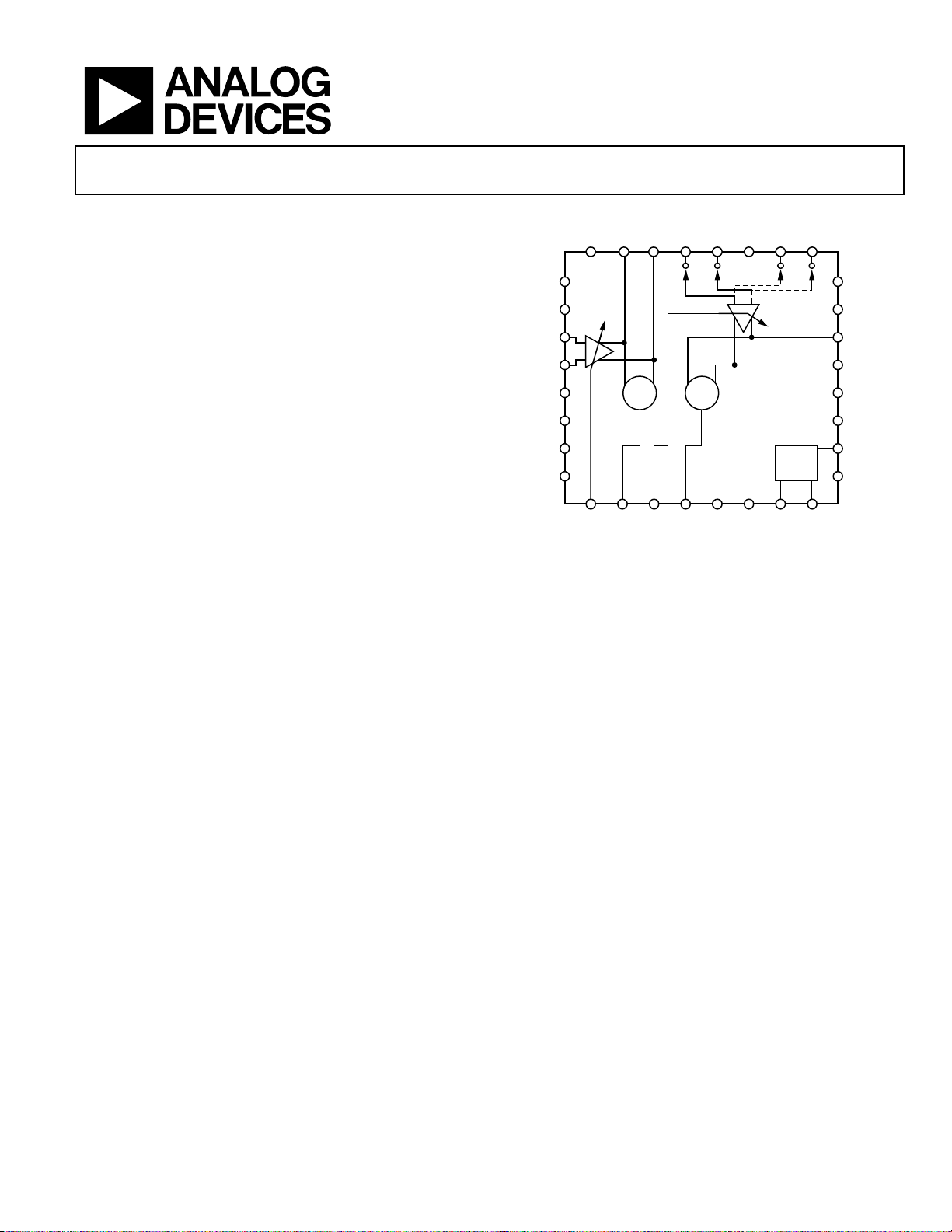
ADL5336
FUNCTIONAL BLOCK DIAGRAM
COM
VCM1
VPOS
INP1
INM1
VPOS
COM
MODE
ENBL
OPP1 OPM1 IP2
VGA1
2
X
GAIN1 DT O1 GAI N2 DTO2 COMD VPSD LE CLK
IM2ACOM IP2B IM2B
2
X
Figure 1.
ADL5336
VGA2
VCM2
VPOS
OPP2
OPM2
VPOS
COM
SDO
SPI
DATA
09550-001
GENERAL DESCRIPTION
The ADL5336 consists of a pair of variable gain amplifiers
(VGAs) designed for cascaded IF applications. The amplifiers
have linear-in-dB gain control and operate from low frequencies to
1 GHz. Their excellent gain conformance over the control range
and flatness over frequency are due to Analog Devices, Inc.,
patented X-AMP® architecture, an innovative technique for
implementing high performance variable gain control.
Each VGA has 24 dB of gain control range. Their maximum gain
can be independently programmable over a 6 dB range via the
SPI. The VGAs can be cascaded to provide a total range of 48 dB.
When connected to a 50 source through a 1:4 balun, the gain
is 6 dB higher. The second VGA has an SPI programmable input
switch that selects one of two external inputs.
When driven from a 200 Ω source or from a 50 Ω source through
a 1:4 balun, the noise figure (NF) for the composite amplifier is
6.8 dB at maximum gain. The output of each VGA can drive
100 Ω loads to 5 V p-p maximum.
Each VGA has an independent square law detector for autonomous,
automatic gain control (AGC) operation. Each detector setpoint
can be programmed independently through the SPI from −24 dBV
to −3 dBV in 3 dB steps. When both VGAs are arranged in AGC
mode and are programmed to the same setpoint, the composite NF
increases to 9 dB when backed off by 18 dB from maximum gain.
The ADL5336 operates from a 5 V supply and consumes a typical
supply current of 80 mA. When disabled, it consumes 4 mA. It is
fabricated in an advanced silicon-germanium BiCMOS process and
is available in a 32-lead exposed paddle LFCSP package. Performance
is specified over a −40°C to +85°C temperature range.
Rev. A
Information furnished by Analog Devices is believed to be accurate and reliable. However, no
responsibility is assumed by Analog Devices for its use, nor for any infringements of patents or other
rights of third parties that may result from its use. Specifications subject to change without notice. No
license is granted by implication or otherwise under any patent or patent rights of Analog Devices.
Trademarks and registered trademarks are the property of their respective owners.
One Technology Way, P.O. Box 9106, Norwood, MA 02062-9106, U.S.A.
Tel: 781.329.4700 www.analog.com
Fax: 781.461.3113 ©2011 Analog Devices, Inc. All rights reserved.
Page 2

ADL5336
TABLE OF CONTENTS
Features.............................................................................................. 1
Applications....................................................................................... 1
Functional Block Diagram ..............................................................1
General Description......................................................................... 1
Revision History ...............................................................................2
Specifications..................................................................................... 3
Timing Diagrams.......................................................................... 5
Absolute Maximum Ratings............................................................ 6
ESD Caution.................................................................................. 6
Pin Configuration and Function Descriptions............................. 7
Typical Performance Characteristics............................................. 8
Theory of Operation ......................................................................17
Circuit Description.....................................................................17
Gain Control Interface............................................................... 18
Input and Output Impedances..................................................18
AGC Operation........................................................................... 18
Register Map and Codes................................................................ 19
Applications Information.............................................................. 20
Basic Connections...................................................................... 20
Supply Decoupling..................................................................... 20
Input Signal Path........................................................................ 20
Output Signal Path..................................................................... 20
Detector Output and Gain Pin................................................. 21
Common-Mode Bypassing....................................................... 21
Serial Port Connections............................................................. 21
Mode and Enable Connections................................................ 21
Error Vector Magnitude (EVM)............................................... 21
Effect of C
AGC Insensitivity to Modulation Type................................... 22
Effect of Setpoint on EVM........................................................ 23
Cascaded VGA/AGC Performance.......................................... 23
Evaluation Board Layout............................................................... 25
Bill of Materials (BOM)............................................................. 27
Evaluation Board Control Software......................................... 28
Outline Dimensions....................................................................... 29
Ordering Guide .......................................................................... 29
on EVM............................................................... 22
AGC
REVISION HISTORY
6/11—Rev. 0 to Rev. A
Changes to Table 1............................................................................ 3
Changes to Typical Performance Charteristics
Section Format.................................................................................. 8
Changes to Figure 7 and Figure 10................................................. 8
Changes to Figure 11 to Figure 16.................................................. 9
Changes to Figure 17 to Figure 22................................................ 10
Changes to Figure 23 and Figure 26............................................. 11
Inserted Figure 53 and Figure 56; Renumbered Sequentially... 16
Changes to Figure 60...................................................................... 17
Changes to Figure 61 Caption....................................................... 18
Changes to Cascaded VGA/AGC Performance Section and
Figure 68 ..........................................................................................24
Changes to Figure 72...................................................................... 26
2/11—Revision 0: Initial Version
Rev. A | Page 2 of 32
Page 3

ADL5336
SPECIFICATIONS
VS = 5 V, TA = 25°C, ZS = 200 Ω, Z
unless otherwise noted. 1:4 balun voltage gain is not included. All dBm numbers are with respect to each VGA’s load impedance.
Table 1.
Parameter Test Conditions/Comments Min Typ Max Unit
OVERALL FUNCTION
Frequency Range
Maximum Input INP1/INM1, IP2A/IM2A, IP2B/IM2B differential 8 V p-p
Maximum Output OPP1/OPM1, OPP2/OPM2 differential at P1dB 5 V p-p
AC Input Impedance
VGA1 Differential across INP1, INM1 200 Ω
VGA2 Selected Input Differential across IP2A, IM2A or IP2B, IM2B 200 Ω
VGA2 Unselected Input 10 kΩ
AC Output Impedance VGA1 1 Ω
VGA2 3.5 Ω
GAIN CONTROL INTERFACE GAIN1/GAIN2, MODE
Voltage Gain Range GAIN1/GAIN2 from 0 V to 1 V
VGA1 Gain Code 00 −14.6 +9.7 dB
Gain Code 01 −12.2 +12 dB
Gain Code 10 −10.3 +13.8 dB
Gain Code 11 −8.9 +15.2 dB
VGA2 Gain Code 00 −10.8 +13.4 dB
Gain Code 01 −8.2 +15.9 dB
Gain Code 10 −6.6 +17.7 dB
Gain Code 11 −4.7 +19.5 dB
Gain Step Response Time 8.5 dB Gain Step 5 ns
Gain Slope
VGA1 MODE = VS 35 mV/dB
VGA2 35 mV/dB
Gain Error V
Input Impedance V
f = 140 MHz
Noise Figure VGA1, Gain Code 00, V
VGA2, Gain Code 11, V
Output IP3 VGA1, Gain Code 00, V
Output Voltage Level of 1.0 V p-p
VGA1, Gain Code 11, V
VGA2, Gain Code 00, V
VGA2, Gain Code 11, V
Output P1dB VGA1, Gain Code 00, V
VGA1, Gain Code 11, V
VGA2, Gain Code 00, V
VGA2, Gain Code 11, V
L VGA1
= 200 Ω, Z
= 100 Ω, RF input = −20 dBm at 140 MHz, maximum gain setting for both VGAs,
L VGA2
3 dB bandwidth LF 1000 MHz
from 0.2 V to 0.8 V ±0.2 dB
GAINx
to COM 4.6 MΩ
GAINx
= 1 V 7.4 dB
GAIN
= 1 V 7.1 dB
GAIN
= 1 V 21 (28) dBV (dBm)
GAIN
= 1 V 18 (25) dBV (dBm)
GAIN
= 1 V 26 (36) dBV (dBm)
GAIN
= 1 V 24 (34) dBV (dBm)
GAIN
= 1 V 3.5(10.5) dBV (dBm)
GAIN
= 1 V 3.5(10.5) dBV (dBm)
GAIN
= 1 V 4 (14) dBV (dBm)
GAIN
= 1 V 4 (14) dBV (dBm)
GAIN
Rev. A | Page 3 of 32
Page 4

ADL5336
Parameter Test Conditions/Comments Min Typ Max Unit
f = 350 MHz
Noise Figure VGA1, Gain Code 00, V
VGA2, Gain Code 11, V
Output IP3 VGA1, Gain Code 00, V
Output Voltage Level of 1.0 V p-p VGA1, Gain Code 11, V
VGA2, Gain Code 00, V
VGA2, Gain Code 11, V
Output P1dB VGA1, Gain Code 00, V
VGA1, Gain Code 11, V
VGA2, Gain Code 00, V
VGA2, Gain Code 11, V
SQUARE LAW DETECTORS DTO1, DTO2
Output Setpoint SPI controlled, 3 dB steps −24 −3 dBV
Output Range 0.1 VS/2 V
AGC Step Response Range 5 dB input step, C
DIGITAL LOGIC LE, CLK, DATA, SDO
Input High Voltage, V
Input Low Voltage, V
Input Current, I
INH/IINL
>2.2 V
INH
<1.8 V
INL
<1 µA
Input Capacitance, CIN 2 pF
SPI TIMING LE, CLK, DATA, SDO
f
20 MHz
CLK
tDH DATA hold time 5 ns
tDS DATA setup time 5 ns
tLH LE hold time 5 ns
tLS LE setup time 5 ns
tPW CLK high pulse width 5 ns
tD CLK-to-SDO delay 5 ns
POWER AND ENABLE VPOS, VPSD, COM, COMD, ENBL
Supply Voltage Range 4.5 5 5.5 V
Total Supply Current ENBL = 5 V 80 mA
Disable Current ENBL = 0 V 4 mA
Disable Threshold 2.3 V
Enable Response Time
Delay following low-to-high transition until
device meets full specifications in VGA mode
Disable Response Time
Delay following high-to-low transition until
device produces full attenuation in VGA mode
= 1 V 8 dB
GAIN
= 1 V 7.7 dB
GAIN
= 1 V 12 (19) dBV (dBm)
GAIN
= 1 V 10.5(17.5) dBV (dBm)
GAIN
= 1 V 18 (28) dBV (dBm)
GAIN
= 1 V 16 (26) dBV (dBm)
GAIN
= 1 V 0 (7) dBV (dBm)
GAIN
= 1 V 0 (7) dBV (dBm)
GAIN
= 1 V −1.5 (+8.5) dBV (dBm)
GAIN
= 1 V −1.5 (+8.5) dBV (dBm)
GAIN
= 0.1 µF 1.5 ms
AGC
800 ns
20 ns
Rev. A | Page 4 of 32
Page 5
ADL5336
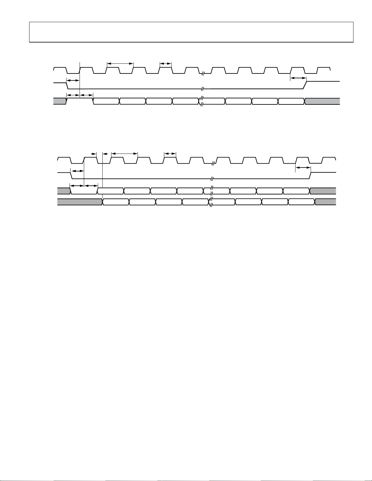
TIMING DIAGRAMS
t
CLK
CLK
LE
DATA
NOTES
1. THE FIRST DATA BIT DETERMINES WHETHER THE PART IS WRITING TO OR READING FROM THE INTERNAL 8-BIT REGISTER. FOR A WRITE
OPERATION, THE FIRST BIT SHOULD BE A LOGIC 1. THE 8-BIT WORD IS THEN REGISTERED INTO THE DATA PIN ON CONSECUTIVE RISING
EDGES OF THE CLOCK.
t
LS
t
t
DS
WRITE BIT
DH
LSB + 1LSB
t
CLK
DCDCREAD BIT DC DC DC DC DC
CLK
DATA
t
D
t
LS
LE
t
t
DH
DS
t
PW
LSB + 2
LSB + 3 MSB – 3 MSB – 2
Figure 2. Write Mode Timing Diagram
t
PW
MSB – 1 MSB
t
LH
09550-002
t
LH
DCDC
SDO
NOTES
1. THE FI RST DATA BIT DETERMINES WHETHER THE PART IS W RITING T O OR READING FROM THE INTERNAL 8- BIT REGI STER. F OR A READ
OPERATIO N, THE FI RST BIT SHOULD BE A LO GIC 0. T HE 8-BIT WO RD IS THEN UPDATED AT THE SDO PIN ON CONSECUTIVE F ALLING EDGES
OF THE CLOCK.
LSB + 1LSB
LSB + 2
LSB + 3 MSB – 3
MSB – 2
MSB – 1 MSB
Figure 3. Read Mode Timing Diagram
09550-003
Rev. A | Page 5 of 32
Page 6
ADL5336
ABSOLUTE MAXIMUM RATINGS
Table 2.
Parameter Rating
Supply Voltages (VPOS, VPSD) 5.5 V
LE, CLK, DATA, SDO VPOS + 0.5 V
ENBL, MODE VPOS + 0.5 V
INP1, INM1, IP2A, IM2A, IP2B, IM2B VPOS + 0.5 V
OPP1, OPM1, OPP2, OPM2 VPOS + 0.5 V
DTO1, DTO2, GAIN1, GAIN2 VPOS/2 + 0.5 V
Internal Power Dissipation 530 mW
θJA (With Pad Soldered to Board) 37.4°C/W
Maximum Junction Temperature 150°C
Operating Temperature Range −40°C to +85°C
Storage Temperature Range −65°C to +150°C
Lead Temperature (Soldering, 60 sec) 300°C
Stresses above those listed under Absolute Maximum Ratings
may cause permanent damage to the device. This is a stress
rating only; functional operation of the device at these or any
other conditions above those indicated in the operational
section of this specification is not implied. Exposure to absolute
maximum rating conditions for extended periods may affect
device reliability.
ESD CAUTION
Rev. A | Page 6 of 32
Page 7
ADL5336
PIN CONFIGURATION AND FUNCTION DESCRIPTIONS
1
IM2B
IP2B
COM
IM2A
IP2A
OPM
OPP1
COM
25
26
27
28
29
30
31
32
1VCM1
PIN 1
2VPOS
INDICATOR
3INP1
4INM1
ADL5336
5VPOS
6COM
TOP VIEW
7MODE
(Not to Scale)
8ENBL
9
11
13
12
10
O2
DT
DTO1
COMD
GAIN2
GAIN1
NOTES
1. EXPOS ED PADDLE. CONNECT TO LOW
IMPEDANCE G ROUND PAD.
24 VCM 2
23 VPOS
22 OPP2
21 OPM2
20 VPOS
19 COM
18 SDO
17 DATA
16
15
14
LE
CLK
VPSD
09550-004
Figure 4. Pin Configuration
Table 3. Pin Function Descriptions
Pin No. Mnemonic Description
1, 24 VCM1, VCM2 Common-Mode Voltages. Decouple to common for ac-coupled operation.
2, 5, 14, 20, 23 VPOS, VPSD Analog and Digital Positive Supply Voltage (4.5 V to 5.5 V).
3, 4, 25, 26, 28, 29
INP1, INM1, IM2B,
Differential Inputs. 200 Ω input impedance; ac coupling recommended.
IP2B, IM2A, IP2A
6, 13, 19, 27, 32 COM, COMD Analog and Digital Common. Connect via lowest possible impedance to external circuit common.
7 MODE Gain Mode Control. Pull high for VGA mode, and pull low for AGC mode.
8 ENBL Chip Enable. Pull high to enable.
9, 11 GAIN1, GAIN2 Analog Gain Control (0 V to 1 V).
10, 12 DTO1, DTO2 Detector Outputs (0.1 V to VPOS/2 Range).
15, 16, 17, 18 LE, CLK, DATA, SDO SPI Programming and Data Readout Pins. CMOS levels V
21, 22, 30, 31
OPM2, OPP2,
Differential Outputs. Low output impedance; ac coupling recommended.
< 1.8 V, V
LOW
HIGH
> 2.2 V.
OPM1, OPP1
EP Exposed Paddle. Connect to low impedance ground pad.
Rev. A | Page 7 of 32
Page 8
ADL5336
T
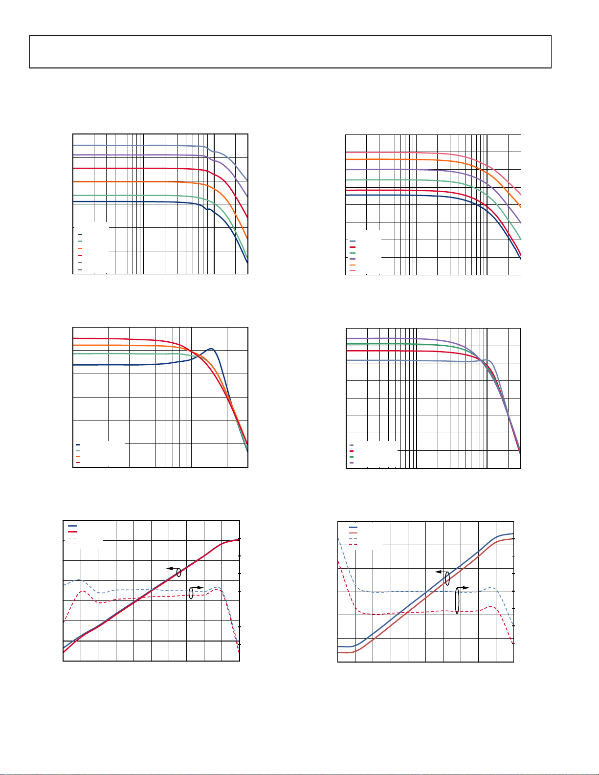
TYPICAL PERFORMANCE CHARACTERISTICS
VS = 5 V, TA = 25°C, ZS = 200 Ω, Z
11, V
= 1 V, setpoint code = 000, MODE = 5 V (VGA mode) for both amplifiers, unless otherwise noted.
GAIN
20
L VGA1
= 200 Ω, Z
= 100 Ω, RF input = −20 dBm at 140 MHz, unless otherwise noted. Gain code =
L VGA2
30
10
0
–10
GAIN1
–20
VOLTAGE GAIN (dB)
Figure 5. Gain vs. Frequency over V
0mV
200mV
400mV
–30
600mV
800mV
1000mV
–40
10M 100M 1G
FREQUENCY ( Hz)
at Gain Code 11 for VGA1
GAIN
5
0
–5
–10
–15
VOLTAGE GAIN (dB)
–20
GAIN CODE 00
GAIN CODE 01
GAIN CODE 10
GAIN CODE 11
–25
100M 1G
FREQUENCY ( Hz)
Figure 6. Gain vs. Frequency over Gain Code at V
20
140MHz
350MHz
140MHz
15
350MHz
10
5
0
VOLTAGE GAIN (dB)
–5
–10
= 0.5 V for VGA1
GAIN
2.0
1.5
1.0
0.5
0
–0.5
–1.0
–1.5
20
10
0
–10
AGE GAIN ( dB)
–20
VOL
GAIN2
–30
0mV
200mV
400mV
–40
600mV
800mV
1000mV
–50
10M 100M 1G
09550-005
Figure 8. Gain vs. Frequency over V
FREQUENC Y (Hz)
at Gain Code 11 for VGA2
GAIN
09550-008
10
5
0
–5
–10
–15
VOLTAGE GAIN (dB)
–20
GAIN CODE 00
GAIN CODE 01
–25
GAIN CODE 10
GAIN CODE 11
–30
10M 100M 1G
09550-006
Figure 9. Gain vs. Frequency over Gain Code at V
FREQUENCY ( Hz)
= 0.5 V for VGA2
GAIN
09550-009
25
20
15
10
ERROR (dB)
VOLTAGE GAIN (dB)
140MHz
350MHz
140MHz
350MHz
5
0
4
3
2
1
0
ERROR (dB)
–1
–2
–3
–15
0 100 200 300 400 500 600 700 800 900 1000
GAIN1 (mV)
Figure 7. Gain vs. V
over Frequency at Gain Code 11 for VGA1
GAIN
–2.0
–5
0 100 200 300 400 500 600 700 800 900 1000
09550-007
Figure 10. Gain vs. V
GAIN1 (mV)
over Frequency at Gain Code 11 for VGA2
GAIN
–4
09550-010
Rev. A | Page 8 of 32
Page 9
ADL5336
T
m
T
20
4
25
4
15
10
5
0
AGE GAIN (dB)
VOL
–5
–10
–15
0 100 200 300 400 500 600 700 800 900 1000
GAIN1 (mV)
–40°C
+25°C
+85°C
–40°C
+25°C
+85°C
Figure 11. Gain Conformance over Temperature for VGA1
35
30
25
20
15
OIP3 (dBm re: 200Ω)
10
5
0
0 100 200 300 4 00 500 600 700 800 900 1000
GAIN1 (mV)
Figure 12. OIP3 vs. V
over Gain Code for VGA1
GAIN
GAIN CODE 11
GAIN CODE 00
30
3
2
1
0
ERROR (dB)
–1
–2
–3
09550-011
20
15
10
5
AGE GAIN ( dB)
VOL
0
–5
–10
0 100 200 300 400 500 600 700 800 900 1000
GAIN1 (mV)
–40°C
+25°C
+85°C
–40°C
+25°C
+85°C
3
2
1
0
ERROR (dB)
–1
–2
–3
–4
09550-014
Figure 14. Gain Conformance over Temperature for VGA2
28
23
18
13
8
OIP3 (dBV)
3
–2
–7
09550-114
40
35
30
25
20
15
OIP3 (d Bm re: 100Ω)
10
5
GAIN CODE 11
GAIN CODE 00
0
0 100 200 300 400 500 600 700 800 900 1000
GAIN2 (mV)
Figure 15. OIP3 vs. V
over Gain Code for VGA2
GAIN
30
25
20
15
10
5
0
–5
–10
OIP3 (dBV)
09550-017
23
40
30
25
20
re: 200Ω)
15
10
OIP3 (dB
5
0
4.54.64.74.84.95.05.15.25.35.45.5
VPOS (V)
Figure 13. OIP3 vs. Supply Voltage at V
= 0.5 V for VGA1
GAIN
18
13
8
OIP3 (dBV)
3
–2
–7
09550-015
35
30
25
20
15
OIP3 (dBm re: 100Ω)
10
5
0
4.5 4.6 4.7 4.8 4.9 5.0 5.1 5.2 5.3 5.4 5.5
VPOS (V)
Figure 16. OIP3 vs. Supply Voltage at V
= 0.5 V for VGA2
GAIN
25
20
15
10
5
0
–5
–10
OIP3 (dBV)
09550-018
Rev. A | Page 9 of 32
Page 10
ADL5336
40
35
30
25
20
15
OIP3 (dBm re: 200Ω)
10
5
0
0 50 100 150 200 250 300 350 400 450 500
FREQUENC Y (MHz)
Figure 17. OIP3 vs. Frequency over Temperature for VGA1
14
GAIN CODE 11
GAIN CODE 00
12
10
8
6
OP1dB (dBm re: 200Ω)
4
2
0
0 0.1 0.2 0.3 0.4 0.5 0.6 0.7 0.8 0.9 1.0
GAIN1 (V)
Figure 18. OP1dB vs. V
over Gain Code for VGA1
GAIN
15
13
11
9
7
5
3
1
OP1dB (d Bm re: 200Ω)
–1
–3
–5
0 50 100 150 200 250 300 350 4 00 450 500
FREQUENC Y (MHz)
Figure 19. OP1dB vs. Frequency over Temperature for VGA1
–40°C
+25°C
+85°C
–40°C
+25°C
+85°C
33
28
23
18
13
8
3
–2
–7
7
5
3
1
–1
–3
–5
–7
8
6
4
2
0
–2
–4
–6
–8
–10
–12
50
45
40
35
30
25
OIP3 (dBV)
09550-013
20
OIP3 (d Bm re: 100Ω)
15
10
5
0
0 50 100 150 200 250 300 350 400 450 500
FREQUENC Y (MHz)
–40°C
+25°C
+85°C
40
35
30
25
20
15
10
5
0
–5
–10
OIP3 (dBV)
09550-016
Figure 20. OIP3 vs. Frequency over Temperature for VGA2
16
14
12
10
8
OP1dB (dBV)
09550-020
6
OP1dB (d Bm re: 100Ω)
4
2
GAIN CODE 11
GAIN CODE 00
0
0 0.10.20.30.40.50.60.70.80.91.0
GAIN2 (V)
Figure 21. OP1dB vs. V
over Gain Code for VGA2
GAIN
6
4
2
0
–2
–4
–6
–8
–10
OP1dB (d BV)
09550-022
16
14
12
10
8
OP1dB (dBV )
09550-019
6
OP1dB (dBm re: 100Ω)
4
2
0
0 50 100 150 200 250 300 350 400 450 500
FREQUENCY (MHz)
–40°C
+25°C
+85°C
6
4
2
0
–2
–4
–6
–8
–10
OP1dB (d BV)
09550-021
Figure 22. OP1dB vs. Frequency over Temperature for VGA2
Rev. A | Page 10 of 32
Page 11

ADL5336
12
5
16
6
10
8
6
4
OP1dB (d Bm re: 200Ω)
2
0
4.54.64.74.84.95.05.15.25.35.45.5
VPOS (V)
Figure 23. OP1dB vs. Supply Voltage for VGA1
40
35
30
25
20
15
NOISE FI GURE (dB)
10
4.5Vdc/–40 °C
5.0Vdc/–40 °C
5.5Vdc/–40 °C
4.5Vdc/+ 25°C
5.0Vdc/+ 25°C
5.5Vdc/+ 25°C
4.5Vdc/+ 85°C
5.0Vdc/+ 85°C
5.5Vdc/+ 85°C
3
1
–1
OP1dB (d BV)
–3
–5
–7
09550-023
14
12
10
8
6
OP1dB (d Bm re: 100Ω)
4
2
0
4.54.64.74.84.95.05.15.25.35.45.5
VPOS (V)
4
2
0
–2
–4
–6
–8
–10
OP1dB (d BV)
9550-026
Figure 26. OP1dB vs. Supply Voltage for VGA2
40
35
30
25
20
15
NOISE FIG URE (dB)
10
4.5Vdc/–40° C
5.0Vdc/–40° C
5.5Vdc/–40° C
4.5Vdc/+ 25°C
5.0Vdc/+ 25°C
5.5Vdc/+ 25°C
4.5Vdc/+ 85°C
5.0Vdc/+ 85°C
5.5Vdc/+ 85°C
5
0
0 0.1 0.2 0.3 0.4 0.5 0.6 0.7 0.8 0.9 1.0
V
(V)
GAIN1
Figure 24. Noise Figure vs. V
over Supply and Temperature for VGA1
GAIN1
13
12
11
10
9
8
7
NOISE FI GURE (dB)
6
5
GAIN CODE 00
GAIN CODE 01
4
GAIN CODE 10
GAIN CODE 11
3
0 100 200 300 400 500 600 700 800
FREQUENC Y (MHz)
Figure 25. Noise Figure vs. Frequency over Maximum Gains for VGA1
5
0
0 0.1 0.2 0.3 0.4 0.5 0.6 0.7 0.8 0.9 1. 0
V
(V)
09550-030
Figure 27. Noise Figure vs. V
GAIN2
over Supply and Temperature for VGA2
GAIN2
09550-031
15
14
13
12
11
10
9
NOISE F IGURE (dB)
8
7
GAIN CODE 00
GAIN CODE 01
6
GAIN CODE 10
GAIN CODE 11
5
9550-033
0 100 200 300 400 500 600 700 800
FREQUENCY (MHz)
09550-034
Figure 28. Noise Figure vs. Frequency over Maximum Gains for VGA2
Rev. A | Page 11 of 32
Page 12

ADL5336
80
70
70
60
50
40
IMD3 (dBc)
30
20
GAIN CODE 11 , 140MHz
GAIN CODE 00 , 140MHz
10
GAIN CODE 00 , 350MHz
GAIN CODE 11 , 350MHz
0
0 100 200 300 400 500 600 700 800 900 1000
GAIN1 (mV)
Figure 29. IMD3 vs. V
over Frequency and Gain Code, V
GAIN
Composite, 2 MHz Spacing for VGA1
GAIN1
RF OUTPUT
= 1 V p-p
OUT
60
50
40
30
IMD3 (dBc)
20
GAIN CODE 00 , 140MHz
10
GAIN CODE 11 , 140MHz
GAIN CODE 00 , 350MHz
GAIN CODE 11 , 350MHz
0
0
100 200 300 400 500 600 700 800 900 1000
09550-029
Figure 32. IMD3 vs. V
GAIN
GAIN2 (mV)
over Frequency and Gain Code, V
= 1 V p-p
OUT
09550-132
Composite, 2 MHz Spacing for VGA2
GAIN2
GAIN2
RF OUTPUT
RF OUTPUT
RF OUTPUT (20mV/DIV ) GAIN1 (100mV/DIV)
TIME (100n s/DIV)
Figure 30. V
Step Response (VGA Mode) over Gain Step, VIN = 100 mV p-p
GAIN
for VGA1
90
80
70
60
50
40
30
SUPPLY CURRENT (mA)
20
10
0
–40 –20 0 20 40 60 80
TEMPERATURE (°C)
Figure 31. Supply Current (VGA1 Switch Disabled) over Temperature
RF OUTPUT (20mV/DIV) GAIN2 (100mV/ DIV)
9550-036
Figure 33. V
Step Response (VGA Mode) over Gain Step, VIN = 100 mV p-p
GAIN
TIME (100ns/ DIV)
09550-039
for VGA2
50
45
40
35
30
25
20
15
SUPPLY CURRENT (mA)
10
5
0
–40 –20 0 20 40 60 80
09550-131
TEMPERATURE (°C)
09550-134
Figure 34. Supply Current (VGA2 Switch Enabled) over Temperature
Rev. A | Page 12 of 32
Page 13

ADL5336
–
250
200
150
100
50
PARALLEL INPUT RESISTANCE (Ω)
GAIN CODE 00
GAIN CODE 11
GAIN CODE 00
GAIN CODE 11
0
10M 100M
FREQUENCY ( Hz)
Figure 35. Input Resistance and Capacitance vs. Frequency for VGA1
0
–5
–10
–15
–20
–25
S11 MAGNITUDE (dB)
–30
–35
–40
0 100 200 300 400 500 600 700 800 900 1000
GAIN1 (mV)
Figure 36. S11 (re: 200 Ω) Magnitude and Phase vs. V
GAIN
2.5
2.0
1.5
1.0
0.5
0
10
–20
–30
–40
–50
–60
–70
–80
–90
for VGA1
PARALLEL INPUT CAPACITANCE (pF)
S11 PHASE (Degrees)
250
200
150
100
50
PARALLEL INPUT RESISTANCE (Ω)
09550-041
GAIN CODE 00
GAIN CODE 11
GAIN CODE 00
GAIN CODE 11
0
10M 100M
FREQUENCY (Hz)
2.5
2.0
1.5
1.0
0.5
0
PARALLEL INPUT CAPACITANCE (pF)
09550-044
Figure 38. Input Resistance and Capacitance vs. Frequency for VGA2
for VGA2
GAIN
–70
–75
–80
–85
–90
–95
–100
–105
–110
–115
–120
S11 PHASE (Degrees)
09550-045
0
–2
–4
–6
–8
–10
–12
S11 MAGNITUDE ( dB)
–14
–16
–18
–20
0 200 400 600 800 1000
09550-042
GAIN2 (mV)
Figure 39. S11 (re: 200 Ω) Magnitude and Phase vs. V
500MHz
3GHz
GAIN CODE 00
GAIN CODE 11
Figure 37. S11 (re: 50 Ω) vs. Frequency over V
10MHz
GAIN
for VGA1
3GHz
GAIN CODE 00
09550-043
GAIN CODE 11
Figure 40. S11 (re: 50 Ω) vs. Frequency over V
500MHz
10MHz
GAIN
for VGA2
09550-046
Rev. A | Page 13 of 32
Page 14

ADL5336
3GHz
500MHz
10MHz
GAIN CODE 00
GAIN CODE 11
Figure 41. S22 (re: 50 Ω) vs. V
over Gain Code for VGA1
GAIN
5
4
3
2
1
0
–1
–2
S22 MAGNITUDE (dB)
–3
–4
–5
0 100 200 300 400 500 600 700 800 900 1000
GAIN1 (mV)
Figure 42. S22 (re: 200 Ω) Magnitude and Phase vs. V
10
GAIN CODE 00
GAIN CODE 11
9
GAIN CODE 00
GAIN CODE 11
8
7
6
5
4
3
2
SERIES OUT PUT RESISTANCE (Ω)
1
0
10M 100M
FREQUENCY (Hz)
Figure 43. Series Output Resistance and Inductance vs.
Frequency over V
for VGA1
GAIN
for VGA1
GAIN
200
190
180
170
160
150
140
130
120
110
100
5
4
3
2
1
0
–1
3GHz
500MHz
10MHz
09550-047
GAIN CODE 00
GAIN CODE 11
Figure 44. S22 (re: 50 Ω) vs. V
over Gain Code for VGA2
GAIN
09550-050
for VGA2
GAIN
180
170
160
150
140
130
120
110
100
90
80
S22 PHASE (Degrees)
09550-051
S22 PHASE (Deg rees)
5
4
3
2
1
0
–1
–2
S22 MAGNITUDE (dB)
–3
–4
–5
0
09550-048
200 400 600 800 1000
GAIN2 (mV)
Figure 45. S22 (re: 100 Ω) Magnitude and Phase vs. V
40
GAIN CODE 00
GAIN CODE 11
GAIN CODE 00
35
GAIN CODE 11
30
25
20
15
10
SERIES OUT PUT INDUCTANCE (nH)
09550-049
SERIES OUT PUT RESISTANCE (Ω)
5
0
10M 100M
FREQUENCY (Hz)
8
7
6
5
4
3
2
1
SERIES OUTPUT INDUCTANCE (nH)
0
–1
09550-052
Figure 46. Series Output Resistance and Inductance vs.
Frequency over V
for VGA2
GAIN
Rev. A | Page 14 of 32
Page 15

ADL5336
RF INPUT
RF INPUT
(500mV/DIV)
DETO1
DETO1
(100mV/DIV)
RF OUTPUT
(500mV/DIV)
RF OUTPUT
TIME (1ms/DIV)
Figure 47. RSSI Step Response (AGC Mode) for VGA1
140 MHz
0.14
350 MHz
0.12
0.10
0.08
(V rms)
OUT
0.06
V
0.04
0.02
RF INPUT
RF INPUT
(200mV/DIV)
DETO2
DETO2
(200mV/DIV)
RF OUTPUT
(200mV/DIV)
09550-053
RF OUTPUT
TIME (1ms/DIV)
9550-056
Figure 50. RSSI Step Response (AGC Mode) for VGA2
0.25
140MHz
350MHz
0.20
0.15
(V rms)
OUT
0.10
V
0.05
0
–50 –45 –40 –35 –30 –25 –20 –15 –10 –5
PIN (dBm)
Figure 48. V
vs. Input Power (PIN) over Frequency (AGC Mode) for VGA1
OUT
0.9
SETPOINT 000
SETPOINT 010
0.8
SETPOINT 100
SETPOINT 110
SETPOINT 001
0.7
SETPOINT 011
SETPOINT 101
SETPOINT 111
0.6
0.5
(V rms)
0.4
OUT
V
0.3
0.2
0.1
0
–40 –35 –30 –25 –20 –15 –10 –5 0 5 10
PIN (dBm)
Figure 49. V
vs. Input Power (PIN) over Setpoint (AGC Mode) for VGA1
OUT
0
–50 –45 –40 –35 –30 –25 –20 –15 –10 –5
09550-148
Figure 51. V
vs. Input Power (PIN) over Frequency (AGC Mode) for VGA2
OUT
PIN (dBm)
09550-151
1.4
SETPOINT 000
SETPOINT 010
SETPOINT 100
1.2
SETPOINT 110
SETPOINT 001
SETPOINT 011
1.0
SETPOINT 101
SETPOINT 111
0.8
(V rms)
0.6
OUT
V
0.4
0.2
0
09550-149
–45 –40 –35 –30 –25 –20 –15 –10 –5 0 5 10
PIN (dBm)
Figure 52. V
vs. Input Power (PIN) over Setpoint (AGC Mode) for VGA2
OUT
09550-152
Rev. A | Page 15 of 32
Page 16

ADL5336
O
T
A
A
0.30
–40°C
+25°C
+85°C
0.25
0.20
0.15
(V rms)
OUT
V
0.10
0.05
0
–55 –50 –45 –40 –35 –30 –25 –20 –15 –10 –5
PIN (dBm)
Figure 53. V
vs. Input Power (PIN) over temperature for VGA1
OUT
0
09550-157
0.20
–40°C
+25°C
0.18
+85°C
0.16
0.14
0.12
0.10
(V rms)
OUT
0.08
V
0.06
0.04
0.02
0
–50 –45 –40 –35 –30 –25 –20 –15 –10 –5
PIN (dBm)
Figure 56. V
vs. Input Power (PIN) over temperature for VGA2
OUT
0
09550-158
–20
–40
TION (dB)
–60
–80
AGE GAIN ISOL
L
V
–100
IN2(a) TO OUT1
–120
10 100
FREQUENCY (MHz)
IN1 TO OUT2
09550-059
Figure 54. Amplifier Isolation vs. Frequency; VGA1 Differential Input (IN1) to
VGA2 Differential Output (OUT2); VGA2 Differential Input A (IN2(a)) to VGA1
Differential Output (OUT1)
80
70
60
50
40
CMRR (dB)
30
20
10
–10
–20
TION (dB)
–30
–40
VOLTAGE GAIN ISOL
–50
–60
10 100
FREQUENC Y (MHz)
IN2(a) TO OUT2
IN2(b) TO OUT2
Figure 57. VGA2 Input Switch Isolation vs. Frequency; VGA2 Disabled
Differential Input (IN2(a), IN2(b)) to VGA2 Differential Output (OUT2)
60
50
40
30
CMRR (dB)
20
10
09550-062
0
10M 100M 1G
FREQUENCY (Hz)
Figure 55. CMRR vs. Frequency for VGA1
09550-154
0
10M 100M 1G
FREQUENCY (Hz)
Figure 58. CMRR vs. Frequency for VGA2
09550-156
Rev. A | Page 16 of 32
Page 17

ADL5336
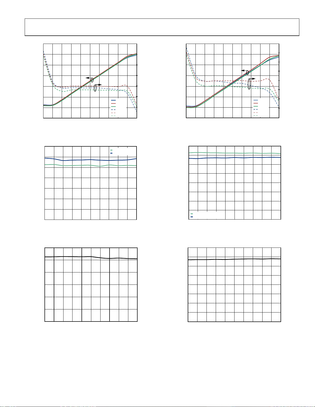
THEORY OF OPERATION
CIRCUIT DESCRIPTION
The ADL5336 contains two differential VGAs, each with a
programmable, internally connected, square law detector. VGA2
includes an input select switch that allows the user to choose
between two sets of differential inputs.
The signal path of each VGA, shown in Figure 59 and Figure 60,
consists of a variable input attenuator followed by a programmable
gain amplifier (PGA).
The input attenuator is built from an 18-section resistor ladder,
providing 1.34 dB of attenuation at each successive tap point.
The resistor ladder acts as a linear input attenuator, in addition
to providing an accurate 200 input impedance. The variable
transconductance (g
signal from the appropriate tap point along the ladder and feed
this signal to the fixed gain amplifier. To realize a continuous
gain control function from discrete tap points, the gain interpolator
creates a weighted sum of signals appearing on adjacent tap points
by carefully controlling the variable g
) stages are used to select the attenuated
m
stages.
m
MODE
The weighted sum of the different tap points is fed into the
programmable gain stage. The programmable gain stage achieves
its different gain settings by changing the feedback network of
the amplifier.
The input attenuator and g
stages provide analog gain control
m
of 24 dB, whereas the programmable gain amplifier sets the
maximum gain of each VGA.
Table 4. VGA Gain Range
Maximum Gain Word
VGA1 VGA2 VGA1 Range (dB) VGA2 Range (dB)
0 0 −14.5 to +9.5 −10 to +14
0 1 −12 to +12.0 −7.1 to +16.9
1 0 −10 to +14.0 −5 to +19
1 1 −8.4 to +15.6 −3.1 to +20.9
GAIN1
INP1
200Ω
INM1
GAIN INTERPO LATOR
gmSTAGES
0dB –1.4dB –2.8dB –23.8dB
ATTENUATOR LADDER
Figure 59. VGA1 Functional Block Diagram
–22.4dB
PGA
PGA LINEAR
VOLTAGE GAIN:
G = 3, 4, 5, 6
OPP1
OPM1
09550-065
MODE
GAIN INTERPOLATOR
gmSTAGES
0dB –1.4dB –2.8dB –23.8dB
ATTENUATOR LADDER
Figure 60. VGA2 Functional Block Diagram
–22.4dB
PGA
PGA LINEAR
VOLTAGE GAIN:
G = 5, 7, 9, 11
OPP2
OPM2
09550-066
IP2A
IP2B
IM2A
IM2B
GAIN2
200Ω
Rev. A | Page 17 of 32
Page 18

ADL5336
GAIN CONTROL INTERFACE
The ADL5336 has a linear-in-dB gain control interface that can
operate in either a gain-up mode or gain-down mode. In the
gain-up mode, with the MODE pin pulled high, the gain increases
with increasing gain voltages. In the gain-down mode, with the
MODE pin pulled low, the gain decreases with increasing gain
voltages. In both modes of operation, the gain control slope is
maintained at +37.5 dB/V or −38 dB/V (depending on mode
selection) over temperature, supply, and process as V
from 100 mV to 900 mV. To form an AGC loop with the on-board
detector around the VGA, the MODE pin has to be pulled low.
Each VGA has 24 dB of gain range that can be shifted as the
maximum gain is programmed.
The gain functions for MODE pulled high and low are given
respectively by
Gain
Gain
where V
25
20
(dB) = 37.5 × V
HIGH
(dB) = −38 × V
LOW
is expressed in volts.
GAIN
GAIN
GAIN
− 14
+ 24.8
GAIN
varies
4
3
AGC OPERATION
The internally connected square law detectors are connected to
the outputs of the VGAs through a programmable attenuator.
The detector compares the output of the attenuator to an
internal reference of 63 mV rms. The AGC loop is closed by
connecting the DTO1/DTO2 pins to the GAIN1/GAIN2 pins,
and having the MODE pin pulled low, configuring the VGAs
for a negative gain slope.
If the attenuator is programmed to pass the full VGA output,
the AGC forces the output of the VGA to 63 mV rms, as long
as the gain required is within the gain range of the VGA. If the
attenuator is programmed to attenuate the VGA output by 21 dB
(Setpoint Word 111) and the AGC loop is closed, the AGC
function forces the VGA output to 707 mV rms. If the gain
required to achieve the programmed target output level is out of
the VGA range, the GAINx pin rails to either VPOS/2 or GND.
If the amplifier is operated in VGA mode or the detector is not
otherwise being used, the setpoint should be programmed to
maximum attenuation so that the VGA output does not overdrive
the input to the detector, adversely affecting both the detector
and VGA output.
15
10
5
GAIN (dB)
0
VGA1 GAIN
–5
–10
–15
0 0.10.20.30.40.50.60.70.80.91.0
Figure 61. Gain and Conformance Error vs. V
VGA1 GAIN
VGA2 GAIN
VGA2 GAIN
VGA1 ERROR
VGA1 ERROR
VGA2 ERROR
VGA2 ERROR
V
GAIN1/VGAIN2
(V)
GAIN1/VGAIN2
for Gain Code 11, and
2
1
0
–1
–2
CONFORM ANCE ERROR (dB)
–3
–4
MODE = 0 V and MODE = 5 V for Both VGAs
INPUT AND OUTPUT IMPEDANCES
The ADL5336 offers differential broadband, 200 Ω input
impedance. The output of each VGA is a low impedance buffer
with negative feedback within the programmable gain amplifier.
The negative feedback reduces the output impedance at low
frequencies, but the output impedance increases with increasing
frequency above 300 MHz.
SPI
SETPOINT
CONTROL
+–
2
X
GAIN1/
GAIN2
9550-067
Figure 62. RMS Detection Diagram (Shows the Signal Path from VGA1/VGA2
Output to Squarer Cell)
DTO1/
DTO2
C
AGC
2
X
REF
63mV rms
09550-073
Rev. A | Page 18 of 32
Page 19

ADL5336
REGISTER MAP AND CODES
Table 5. Register Map
MSB
B10 B9 B8 B7 B6 B5 B4 B3 B2 B1 B0
VGA2 Maximum Gain VGA1 Maximum Gain VGA2 Switch VGA2 Setpoint VGA1 Setpoint
Table 6. RMS Output Setpoint Map
0 0 0 +62.5/−24
0 0 1 +88/−21
0 1 0 +125/−18
0 1 1 +176/−15
1 0 0 +250/−12
1 0 1 +353/−9
1 1 0 +500/−6
1 1 1 +707/−3
Table 7. VGA2 Input Switch Logic
VGA2 Switch Selected Input
0 IP2A, IM2A
1 IP2B, IM2B
Setpoint Word RMS Output (mV rms/dBV)
LSB
Table 8. Maximum Gain Map
Maximum Gain Word VGA1 Maximum Gain (dB) VGA2 Maximum Gain (dB)
0 0 9.5 14
0 1 12.0 16.9
1 0 14.0 19
1 1 15.6 20.9
Rev. A | Page 19 of 32
Page 20

ADL5336
APPLICATIONS INFORMATION
BASIC CONNECTIONS INPUT SIGNAL PATH
The basic connections for a typical ADL5336 application are
shown in Figure 63.
SUPPLY DECOUPLING
A nominal supply voltage of 5.0 V should be applied to the supply
pins. The supply voltage should be between the limits of 4.5 V
and 5.5 V. All of the supply pins must be decoupled to ground
with at least one low inductance, surface-mount ceramic capacitor
of 0.1 µF. Place these decoupling capacitors as close as possible
to the ADL5336 device. The ADL5336 has an analog supply and
a digital supply. Take care to separate the two supplies with a
large surface-mount inductor of 33 µH, and each supply must
then be decoupled separately to their respective grounds through a
10 µF capacitor. The ADL5336 also has two separate grounds: an
analog ground and a digital ground. Again, a large surface-mount
inductor of 33 µH should be used to separate the grounds.
The ADL5336 has three input signal paths, two of which inputs
go to VGA2 via an internal switch, and the other input goes to
VGA1. Each of the three pairs of input pins (INP1/INM1,
IP2A/IM2A, and IP2B/IM2B) has a differential input impedance of
200 Ω. To obtain maximum power transfer, the driving source
impedance also needs to be 200 Ω. On the evaluation board,
this is achieved via a 4:1 impedance ratio balun. The evaluation
board schematic is shown in Figure 70. For more information
on the input signal paths, refer to the Input Signal Path section.
The input common-mode voltage sits at roughly VPOS/2 for
both VGAs, except on VGA2; the nonselected input of VGA2
has an input common-mode voltage that sits at roughly ground.
OUTPUT SIGNAL PATH
There are two output signal paths on the ADL5336; one signal
path per VGA. The output of VGA1 can be ac-coupled into either
of the inputs of VGA2, which cascades the two VGAs, or ac-coupled
into a 200 Ω termination impedance. VGA1 is designed to drive a
200 Ω differential load, whereas VGA2 is designed to drive a 100 Ω
differential load. On the evaluation board, a 100 Ω differential
impedance is presented to the output of VGA2. This is achieve
via a 1:1 balun and a resistive matching network. For more
information on the evaluation board, see the evaluation board
schematic in Figure 70. The output common-mode voltage on
both VGAs sits at roughly VPOS/2.
OPP1
DTO1
INPUT 2
BALUN
IP2A
OPM1
ADL5336
GAIN2
DTO2
INPUT 3
BALUN
IP2B
COM
IM2A
COMD
VPSD
IM2B
VCM2
VPOS
OPP2
OPM2
VPOS
COM
SDO
DATA
CLK
LE
INPUT 3
+5V
OUTPUT 2
BALUN
SPI CO NTROL
OUTPUT 2
09550-075
INPUT 1
VPOS
VPOS
INPUT 2
OUTPUT 1
+5V
INPUT 1
BALUN
+5V +5V
OUTPUT 1
BALUN
COM
VCM1
VPOS
INP1
INM1
VPOS
COM
MODE
ENBL
GAIN1
Figure 63. Basic Connections Schematic
Rev. A | Page 20 of 32
Page 21

ADL5336
DETECTOR OUTPUT AND GAIN PIN
The ADL5336 has a pair of detector squaring cells. Each squaring
cell has a VGA output applied to its input. This is shown Figure 1
and Figure 62. These on-board detector squaring cells are used to
achieve an AGC function with the VGAs. Each of the squared
output signals is compared to a reference signal and the difference
is then output in a current-mode signal. The DTO1 pin is the
detector squaring cell output that taps off of the output VGA1,
and the DTO2 pin is the detector squaring cell output that taps
off of the output of VGA2. By shorting the DTO1 and GAIN1
pins together and putting a capacitor to ground on the DTO1/
GAIN1 node, the AGC function can be achieved using VGA1.
The same connections can be done to DTO2 and GAIN2 to
achieve the AGC function using VGA2. The MODE pin must
be pulled low for the AGC function. For more information on
the detector squaring cells and the AGC function, refer to the
AGC Operation section. For information concerning the capacitor
value used, refer to the Theory of Operation section.
COMMON-MODE BYPASSING
Decouple the two common-mode pins, VCM1 (Pin 1) and VCM2
(Pin 24), of the ADL5336 using low inductance, surface-mount
ceramic capacitors. The evaluation board has 0.1 µF capacitor
values for each of the common-mode pins (see Figure 70).
SERIAL PORT CONNECTIONS
The SPI port of the ADL5336 writes data into the device and
reads data out of it. The SPI port controls maximum VGA gain
levels, output setpoint levels, and VGA2 input selection. It is
recommended to put low-pass RC filtering on the SPI lines to
filter out any high frequency glitches if reading and writing to the
SPI port becomes problematic. Capacitors C26 through C29,
shown in Figure 70, can be populated, along with replacing the
standard 0 Ω jumper resistors (R9 to R12) to make an
appropriate low-pass RC filter network on each SPI line.
MODE AND ENABLE CONNECTIONS
The ADL5336 can have both a positive and negative gain slope.
This function is controlled by the MODE pin. When the MODE
is pulled high, it puts each VGA into traditional VGA mode, where
the gain slope is positive. When the MODE pin is pulled to
ground, both VGAs have a negative gain slope, which is needed
to obtain an AGC function with either VGA. The MODE
threshold voltage levels are: V
slope and V
Pulling the ENBL pin high enables the part and allows for normal
operation. If the ENBL pin is pulled low, then the ADL5336 powers
down and only draws approximately 4 mA of supply current.
< 2 V for the negative gain slope.
MODE
> 3 V for the positive gain
MODE
ERROR VECTOR MAGNITUDE (EVM)
EVM is a measure used to quantify the performance of a digital
radio transmitter or receiver by measuring the fidelity of the digital
signal transmitted or received. Various imperfections in the link,
such as magnitude and phase imbalance, noise, and distortion,
cause the constellation points to deviate from their ideal locations.
In general, as signal power increases, the distortion components
increase. A typical receiver exhibits the three following distinct
EVM limitations vs. the received input signal power:
• At large enough signal levels, where the distortion
components due to the harmonic nonlinearities in the
device are falling in-band, EVM degrades as signal levels
increase.
• At medium signal levels, where the signal chain behaves in
a linear manner and the signal is well above any notable noise
contributions, EVM has a tendency to reach an optimal level
determined dominantly by either the quadrature accuracy
and I/Q gain match of the signal chain or the precision of
the test equipment.
• As signal levels decrease, such that noise is a major
contributor, EVM performance vs. the signal level exhibits
a decibel-for-decibel degradation with decreasing signal
level. At these lower signal levels, where noise is the dominant
limitation, decibel EVM is directly proportional to the SNR.
Rev. A | Page 21 of 32
Page 22

ADL5336
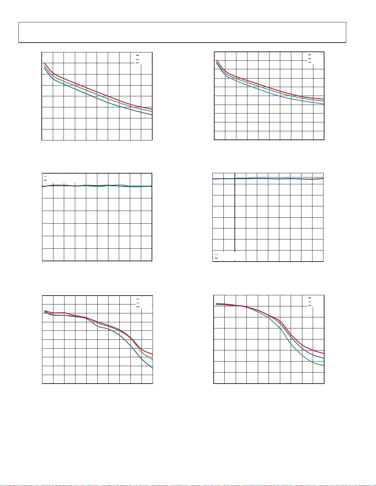
EFFECT OF C
The choice of C
response time, and carrier leakage. If C
small to speed up the response time, the AGC loop could start
tracking and leveling any amplitude envelope and corrupt the
constellation. The AGC loop bandwidth (BW) is given by the
equation
BW
LOOP
where R
By increasing C
improved because the signal is outside of the AGC loop BW,
and therefore, the AGC no longer levels the amplitude envelope
of the signal. Figure 64 illustrates this behavior with three different
AGC capacitor values while the ADL5336 VGAs are cascaded.
There is a drastic degradation of EVM when the smaller capacitor
values are used. This example uses a 16 QAM modulated signal
at 4.5 Msym/sec using a pulse shaping filter and an alpha of
0.35. The frequency used was 140 MHz and output setpoints for
both VGAs were 250 mV rms. Both VGAs were set to maximum
gain codes of 11.
is the on-chip equivalent resistance of the loop.
AGC
0
–5
–10
–15
–20
–25
EVM (dB)
–30
–35
–40
–45
–50
–65 –55 –45 –35 –25 –15 –5 5 15 25
Figure 64. EVM vs. RF Input Power over Several C
ON EVM
AGC
is a compromise of averaging time constant,
AGC
is selected to be too
AGC
= 1/(2π × R
(which decreases the loop BW), EVM can be
AGC
C
= 0.1µF
AGC
= 1000pF
C
AGC
= 100pF
C
AGC
× C
AGC
)
AGC
RF INPUT POWER (dBm)
AGC
Values
AGC INSENSITIVITY TO MODULATION TYPE
Given that C
modulated signal and carrier frequency, EVM should not degrade
much with different modulation types. The four different
modulation types, and how EVM changes with each, are shown in
Figure 65. There is an approximately 4 dB spread across the curves.
All modulated signals were set to 4.5 Msym/sec using a pulse
shaping filter and an alpha of 0.35. The frequency used was
140 MHz. C
250 mV rms. Both VGAs were set to maximum gain codes of 11.
09550-072
Rev. A | Page 22 of 32
is chosen correctly for the symbol rate of the
AGC
= 0.1 µF and output setpoints for both VGAs were
AGC
0
–5
–10
–15
–20
–25
EVM (dB)
–30
–35
–40
–45
–50
–65 –55 –45 –35 –25 –15 –5 5 15 25
RF INPUT P OWER (d Bm)
Figure 65. EVM vs. RF Input Power Over Several Modulation Types
16QAM
256QAM
QPSK
8PSK
09550-070
Page 23

ADL5336
EFFECT OF SETPOINT ON EVM CASCADED VGA/AGC PERFORMANCE
While in AGC mode, the EVM can degrade depending on the
output setpoint each VGA is set to. There is a strong relationship
between the output setpoint of VGA2 and EVM performance
while the output setpoint of VGA1 is held constant. Conversely,
the EVM does not change much while the output setpoint of the
VGA2 is held constant and the output setpoint of VGA1 is
changed. This behavior can be seen in Figure 66 where several
different setpoints of both VGAs were tested. This example uses
a 16 QAM modulated signal at 4.5 Msym/sec using a pulse
shaping filter and an alpha of 0.35.The frequency used was 140
MHz and C
= 0.1 µF. Both VGAs were set to maximum gain
AGC
codes of 11.
0
VGA1 88mV rms, VGA2 250mV rms
VGA1 250mV rms, VGA2 250mV rms
–5
VGA1 707mV rms, VGA2 250mV rms
VGA1 250mV rms, VGA2 88mV rms
–10
VGA1 250mV rms, VGA2 500mV rms
VGA1 250mV rms, VGA2 125mV rms
–15
VGA1 250mV rms, VGA2 176mV rms
–20
–25
EVM (dB)
–30
–35
–40
–45
–50
–65 –55 –45 –35 –25 –15 –5 5 15 25
RF INPUT P OWER (d Bm)
Figure 66. EVM vs. RF Input Power over Several Setpoints
0
VGA2 88mV rms
VGA2 125mV rms
–5
VGA2 176 mV rms
VGA2 250mV rms
VGA2 500mV rms
–10
VGAIN2 250/88
VGAIN2 250/125
VGAIN2 250/176
–15
VGAIN2 250/250
VGAIN2 250/500
–20
–25
EVM (dB)
–30
–35
–40
–45
–50
–65 –55 –45 –35 –25 –15 –5 5 15 25
RF INPUT POWER (d Bm)
V
GAIN1
Figure 67. EVM vs. RF Input Power While VGA1 Setpoint Held Constant to
250 mV rms and VGA2 Setpoint Swept; VGA1/VGA2 Gain Code = 11
2.5
2.0
1.5
1.0
0.5
0
09550-071
(V)
/V
V
GAIN2
GAIN1
09550-165
The ADL5336 is designed for easy cascading of the two VGAs.
Cascading VGAs decreases the overall noise figure by keeping
as much gain as possible before the final gain stage/noise source. A
single X-AMP has constant output referred noise. For an 8 dB
NF amplifier, with 36 dB maximum gain, in a 200 Ω matched
system, output referred noise V
= 144 nV/√Hz. RTO, the
N, RTO
noise contribution from the source, is the constant source noise
multiplied by the gain (as the gain is reduced, the noise contribution
from the source decreases). Measuring noise figure as 20 × log10
(total noise/noise from source), the dB-for-dB degradation in
NF typical of this architecture can be seen.
When the gain is partitioned into two VGAs, consider 18 dB
each. If each has an 8 dB NF, then each has an RTO noise of
18 nV/√Hz, including the source noise, and 16.5 nV/√Hz,
excluding the source noise. At maximum gain, the total RTO
noise is 145 nV/√Hz. As overall gain is decreased, the gain of
VGA2 is decreased first. When the gain of VGA2 is decreased
by 6 dB, the noise contributions from the source and VGA1
both decrease by 6 dB for an overall RTO noise of the system
that falls to 74 nV/√Hz.
When VGA1 and VGA2 are cascaded and operating in AGC
mode, setpoint programming affects dynamic range. The noise
measured at the output of VGA1 is relatively constant across
gain, which is a feature common to X-AMP VGAs. However,
measured at the output of VGA2, the noise contribution from
VGA2 is constant, but the noise contribution from VGA1 depends
on the gain of VGA2. For a given overall gain (VGA1 and VGA2),
the gain partitioning between VGA1 and VGA2 controls total
RTO noise and distortion.
To illustrate, consider the case where both VGAs are programmed
to a maximum gain of 14 dB and the setpoint of VGA2 is 101,
or 353 mV rms. Gain and signal levels can also be looked at
when the setpoint of VGA1 is programmed to 011, 101, and
111, 176 mV rms, 353 mV rms, and 707 mV rms (see Tabl e 9).
Table 9. Total Cascaded Output Noise
Vi (mV rms) AV1 (dB) VO1 (mV rms) AV2 (dB) VO (mV rms) n1 n2 n
TOTAL
176 0 176 +6 353 20 10 22.4
176 6 353 0 353 10 10 14.1
176 12 707 −6 353 5 10 11.2
Rev. A | Page 23 of 32
Page 24

ADL5336
As the setpoint of VGA1 increases, the total output noise decreases.
Linearity limits how high the setpoint of VGA1 for a given
system can be programmed. For two equal sinusoidal tones,
353 mV rms corresponds to 1.4 V p-p, whereas 707 mV rms
corresponds to 2.8 V p-p. For a 1.4 V p-p composite output,
IMD3 is approximately −65 dBc; however, for a 2.8 V p-p
composite output, IMD3 is theoretically 12 dB worse at −53 dBc.
For each VGA, total RTO noise increases at higher maximumgain settings; therefore, the overall combination of maximum
gain should be minimized while still satisfying all system
requirements with adequate margin.
In linear terms, the noise figure of the cascaded amplifiers can
be given by
NF
CAS
= NF
VGA1
+ (NF
VGA2
− 1)/G
VGA1
Because both VGAs are X-AMPs, the noise figure of each VGA
degrades dB-for-dB as the gain of each VGA decreases. This is
due to the attenuation ladder on the input that attenuates the
signal before the signal is gained up. If only the gain of the second
VGA is changing, the cascaded noise figure does not change
appreciably because the noise figure of the second VGA is being
divided by the constant gain of the first VGA. When the gain of
VGA2 drops to the minimum and the input signal level is still
decreasing, VGA1 takes over and its gain starts to change. The
cascaded noise figure increases dB-for-dB while the gain of VGA1
decreases.
While cascading the VGAs, keeping intermodulation distortion
components low is at direct odds with keeping noise figure and
output noise density low. It can be shown that the third-order
intercept of a cascaded system in linear terms is
P3 = 1/(1/(G
where P
3_VGA1
and P
VGA2P3_VGA1
3_VGA2
) + 1/P
3_VGA2
)
are the third-order intercept points of
each VGA in watts. Thus, when the overall IP3 is the largest
(distortion is the smallest), the gain of VGA2 is at its maximum.
Vice-versa, when the gain of VGA2 is at its minimum, the
overall IP3 is the smallest, and distortion is at its maximum.
Table 10 provides conditions for optimization for the output
noise density, noise figure, and distortion parameters.
Table 10. Optimized Conditions
VGA1 Gain VGA2 Gain
Output Noise
Noise Figure
IMD/IP3
1
Having the gain of VGA2 at maximum does not change the overall noise
figure much due to the noise figure contribution of VGA2 being divided by
the gain of VGA1.
2
IMD levels do not change much over the X-Amp gain range, but best IMD
levels are achieved at high gains.
Minimum Minimum
Maximum Maximum1
Maximum
2
Maximum
When starting from a very small input power, such that neither
VGA has reached their respective setpoints, and the analog gain
of both VGAs is forced to its maximum, the cascaded OIP3 is at
its maximum, while the cascaded noise figure is at its minimum.
As the input power is increased, each VGA keeps its gain at
maximum until its respective setpoint is reached, at which point
the gain of the VGA (whose setpoint has been reached) decreases
to accomodate the increaced input power and thus changes the
cascaded OIP3 and noise figure.
Figure 68 shows how the OIP3 changes while input power is
varied in AGC mode, which consequently changes the analog
gains of the VGAs. The setpoint of VGA2 is fixed to 100 (or
250 mV rms), and the setpoint of VGA1 is changed from 001
(88 mV rms) to 100 (250 mV rms), and finally, to 111
(707 mV rms).
35
30
25
20
OIP3 (dBm re: 100Ω)
15
10
–20–15–10–5 0 5 1015202530
OVERALL VOLTAGE GAIN (d B)
Figure 68. OIP3 vs. Overall Voltage Gain over Several Setpoints;
VGA1 Gain Code = 11 and VGA2 Gain Code = 00
60
50
40
30
20
NOISE F IGURE ( dB)
10
0
–20 –10 0 10 20 30
OVERALL VOLTAGE GAIN (dB)
Figure 69. Noise Figure vs. Overall Voltage Gain over Several Setpoints;
VGA1 Gain Code = 11 and VGA2 Gain Code = 00
LOW TONE, SETPOINT = 001
HIGH TONE, SETPOINT = 001
LOW TONE, SETPOINT = 100
HIGH TONE, SETPOINT = 100
LOW TONE, SETPOINT = 111
HIGH TONE, SETPOINT = 111
SETPOINT = 001
SETPOINT = 100
SETPOINT = 111
25
20
15
OIP3 (dBV)
10
5
0
09550-076
09550-077
Figure 69 shows how the NF changes while the input power is
varied in AGC, which again, consequently changes the analog
gains of the VGAs. The setpoint of VGA2 is still fixed to 100
(250 mV rms), and the changes made to the setpoint of VGA1
is the same as before.
Rev. A | Page 24 of 32
Page 25

ADL5336
EVALUATION BOARD LAYOUT
An evaluation board is available for testing the ADL5336. The evaluation board schematic is shown in Figure 70. Tabl e 11 provides the
component values and suggestions for modifying the component values for the various modes of operation.
C1
R4
OPEN
0.1µF
VPOS
C24
L2
33µH
L1
33µH
OPEN
2
C19
0.1µF
C20
0.1µF
3
1
VPOSVPOSD
R13
T4
4
6
24.9Ω
37.4Ω
37.4Ω
SDO
C2
10µF
R5
R6
VPOSVPSD
INPUT3
R7
T3
R8
24.9Ω
COM
OUTPUT2
51
4
3
R10
0Ω
C29
OPEN
INPUT1
T1
61
2
43
C21
0.1µF
VPOS
VPOS
OUTPUT1
VCM1
VPOS
C3
0.1µF
C4
0.1µF
VPOS
P2
P3
C7
0.1µF
C5
0.1µF
0.1µF
INPUT2
4
T5
3
1
2
R14
OPEN
T2
661
4
C22
0.1µF
C6
C8
0.1µF
2
3
C9
0.1µF
R15
OPEN
VCM1
VPOS
INP1
INM1
VPOS
COM
MODE
ENBL
C23
0.1µF
COM
OPP1
OPM1
C11
C10
0.1µF
0.1µF
IP2A
IP2B
COM
IM2A
ADL5336
GAIN2
DTO1
GAIN1
DTO2
LE
COMD
VPSD
C14
0.1µF
IM2B
VCM2
VPOS
OPP2
OPM2
VPOS
DATA
CLK
COM
SDO
COMD
C15
0.1µF
OPEN
VPOS
DATA
R3
VCM2
C25
0.1µF
C17
0.1µF
C28
OPEN
10µF
C18
0.1µF
R11
0Ω
GAIN1
NET NAME
TEST POINT
SMA INPUT/OUTPUT
DIGITAL GROUND
ANALOG G ROUND
JUMPER
P5
R1
0Ω
C12
0.1µF
GAIN2
P4
C13
0.1µF
11421531641751861972082192210231124122513
P1
C16
0.1µF
LE
C26
OPEN
R2
0Ω
R9
CLK
0Ω
VPSD
C27
OPEN
R12
0Ω
ENBLVPOS
GAIN2
GAIN1
09550-081
Figure 70. Evaluation Board Schematic
Rev. A | Page 25 of 32
Page 26

ADL5336
09550-082
Figure 71. Silkscreen Top
09550-082
Figure 72. Silkscreen Bottom
Rev. A | Page 26 of 32
Page 27

ADL5336
BILL OF MATERIALS (BOM)
Table 11. Evaluation Board Configuration Options
Components Function Default Conditions
C1, C2, C5, C6, C7, C16, C17,
C18, C25, L1, L2
C3, C4, C21, T1
C10, C11, C14, C15, C23, C24,
R3, R4, R13, T4, T5
C8, C9, C22, R14, R15, T2
C19, C20, R5, R6, R7, R8, T3
R1, C12
R2, C13
P3
P2
R9, R10, R11, R12, C26, C27,
C28, C29, P1
P5
P4
Power supply and ground decoupling. Nominal supply
decoupling consists of 0.1 µF capacitor to ground.
VGA1 input interface. The balun T1 has a 4:1 impedance ratio that
transforms a single-ended signal in a 50 Ω system into a
differential signal in a 200 Ω system. C3 and C4 provide ac
coupling into VGA1, and C21 provides an ac ground for the balun.
VGA2 input interface. The T4 and T5 baluns have 4:1 impedance
ratios that transform single-ended signals in a 50 Ω system into
differential signals in a 200 Ω system. The user has a choice of
either Input A or Input B, which is set by Bit B6 in the internal
register (see the register map in Table 5). C11, C14, C15, and C23
provide ac coupling into VGA2, and C10 and C24 provide an ac
ground for the baluns. R3, R4, and R13 are left open by default. AC
ground can be achieve by placing 0 Ω jumpers at R3 and R4. A
0 Ω jumper can be installed at R13 to drive Input B of VGA2 single
ended. Note that R4 must be open and R3 must have a 0 Ω
jumper installed.
VGA1 output interface. The T2 balun has a 4:1 impedance ratio
that transforms a differential signal in a 200 Ω system into a
single-ended signal in a 50 Ω system. C8 and C9 provide ac
coupling out of VGA1, and C22 provides an ac ground for the
balun. R14 and R15 can be made 0 Ω and dc-couple the output of
VGA1 into the input of VGA2 in cascading applications.
VGA2 output interface. The transmission line transformer, T3, has
a 1:1 impedance ratio that transforms a differential signal to a
single-ended signal. The 50 Ω impedance is the same on both the
primary and secondary side balun. C19 and C20 provide ac
coupling out of VGA2. R5, R6, R7, and R8 raise the impedance that
the output of VGA2 sees to 100 Ω differential.
Detector 1 interface. R1 serves as a 0 Ω jumper to connect the
integrating capacitor, C12, that is needed when VGA1 is being
used in AGC mode.
Detector 2 interface. R2 serves as a 0 Ω jumper to connect the
integrating capacitor, C13, that is needed when VGA2 is being
used in AGC mode.
Enable interface. The ADL5336 is powered up by applying a logic
high voltage to the ENBL pin. Jumper P3 is connected to VPOS.
MODE interface. The MODE pin must be pulled to a logic high to
be used in VGA mode. If AGC mode is desired, a logic low must be
applied to the MODE pin. The P2 jumper must be connected to
either VPOS (logic high) or ground (logic low).
Serial control interface. The digital interface sets the VGA1
setpoint, VGA2 setpoint, VGA2 input selection, VGA1 maximum
gain, and the VGA2 maximum gain of the device using the serial
interface lines CLK, LE, DATA, and SDO. RC filter networks are
provided on CLK and LE lines to filter the PC signals (possibly on
all the lines). CLK, DATA, SDO, and LE signals can be observed via
SMB connectors for debug purposes.
Analog VGA1 gain control. The range of the GAIN1 pin is from 0 V
to 1 V, creating a gain scaling of 35 mV/dB.
Analog VGA2 gain control. The range of the GAIN2 pin is from 0 V
to 1 V, creating a gain scaling of 35 mV/dB.
C1, C2 = 10 µF (0805),
C5, C6, C7, C16, C17 = 0.1 µF (0402),
C18, C25 = 0.1 µF (0402),
L1, L2 = 33 H (0805)
C3, C4, C21 = 0.1 µF (0402),
T1 = Mini-Circuits TC4-1W
C10, C11, C14 = 0.1 µF (0402),
C15, C23, C24 = 0.1 µF (0402),
R3, R4, R13 = open (0402),
T4, T5 = Mini-Circuits TC4-1W
C8, C9, C22 = 0.1 µF (0402),
R14, R15 = open (0402),
T2 = Mini-Circuits TC4-1W
C19, C20 = 0.1 µF (0402),
R5, R6 = 37.4 Ω (0402),
R7, R8 = 24.9 Ω (0402),
T3 = M/A-COM ETC1-1-13
R1 = 0 Ω (0402),
C12 = 0.1 µF (0402)
R2 = 0 Ω (0402),
C13 = 0.1 µF (0402)
P3 = installed for enable
P2 = installed
R9, R10, R11, R12 = 0 Ω (0402),
C26, C27, C28, C29 = open (0402),
P1 installed,
SMB connectors installed
P5 installed
P4 installed
Rev. A | Page 27 of 32
Page 28

ADL5336
EVALUATION BOARD CONTROL SOFTWARE
The ADL5336 evaluation board is controlled through the parallel
port on a PC. The parallel port is programmed via the ADL5336
evaluation software. This software controls the following:
• The setpoints of VGA1 and VGA2
• The maximum gains of VGA1 and VGA2
• The input control switch of VGA2
For information about the register map, see Tabl e 5, Ta ble 6,
Table 7, and Tabl e 8. For information about SPI port timing and
control, see Figure 2 and Figure 3.
After the software is downloaded and installed, start the basic user
interface to program the maximum gains, setpoints, and the input
of VGA2, see Figure 73.
To program the setpoints of each VGA, click on the respective pulldown menu of the desired VGA under RMS Out (mVrms/dBV),
select the desired setpoint, and click Wr it e B its .
To program the maximum gain of each VGA, click on the respective
pull-down menu of the desired VGA under the VGA 1 Max
Gain (dB)/VGA 2 Max Gain (dB), select the desired maximum
gain, and click Write B its .
When the user clicks Write B i ts , a write operation executes,
immediately followed by a read operation. The updated
information is displayed in the VGA1 Current State and VGA 2
Current State fields. The gain displayed does not represent the
analog VGA gain, only the digital maximum gain.
On VGA2, the user can switch to either Input A or Input B by
selecting the slider switch, VGA 2 Switch.
Because the speed of the parallel port varies from PC to PC, the
Clock Stretch function can be used to change the effective frequency
of the CLK line. The CLK line has a scalar range from 1 to 10;
10 is the fastest speed, and 1 is the slowest.
09550-084
Figure 73. ADL5336 Software Screen Capture
Rev. A | Page 28 of 32
Page 29

ADL5336
OUTLINE DIMENSIONS
0.08
0.60 MAX
25
24
EXPOSED
PAD
(BOTTOM VIEW)
17
16
3.50 REF
PIN 1
32
9
FORPROPERCONNECTIONOF
THE EXPOSED PAD, REFER TO
THE PIN CONFIGURATION AND
FUNCTION DESCRIPTIONS
SECTION OF THIS DATA SHEET.
INDICATOR
1
3.25
3.10 SQ
2.95
8
0.25 MIN
011708-A
5.00
PIN 1
INDICATOR
1.00
0.85
0.80
12° MAX
SEATING
PLANE
BSC SQ
TOP
VIEW
0.80 MAX
0.65 TYP
0.30
0.23
0.18
COMPLIANT TO JEDEC STANDARDS MO-220-VHHD-2
4.75
BSC SQ
0.20 REF
0.05 MAX
0.02 NOM
0.60 MAX
0.50
BSC
0.50
0.40
0.30
COPLANARITY
Figure 74. 32-Lead Lead Frame Chip Scale Package [LFCSP_VQ]
5 mm × 5 mm Body, Very Thin Quad
(CP-32-2)
Dimensions shown in millimeters
ORDERING GUIDE
Model1 Temperature Range Package Description Package Option
ADL5336ACPZ-R7
ADL5336-EVALZ Evaluation Board
1
Z = RoHS Compliant Part.
−40°C to +85°C 32-Lead LFCSP_VQ, 7” Tape and Reel CP-32-2
Rev. A | Page 29 of 32
Page 30

ADL5336
NOTES
Rev. A | Page 30 of 32
Page 31

ADL5336
NOTES
Rev. A | Page 31 of 32
Page 32

ADL5336
NOTES
©2011 Analog Devices, Inc. All rights reserved. Trademarks and
registered trademarks are the property of their respective owners.
D09550-0-6/11(A)
Rev. A | Page 32 of 32
 Loading...