

Page 1
1 MHz - 3 GHz VGA with
a
60dB Gain Control Range
Preliminary Technical Data ADL5330
FEATURES
Voltage-Controlled Amplifier/Attenuator
Operating Frequency 1 MHz to 3 GHz
Optimized for Controlling Output Power
High Linearity: OIP3 31 dBm @ 900 MHz
Output Noise Floor -150 dBm/Hz @ 900 MHz
Fully-Balanced Differential Signal Path
Differential Input at 50 Ω
Wide Gain-Control Range: -34 dB to +22 dB @ 900 MHz
Linear-in-dB Gain Control Function, 20 mV/dB
Single Supply 4.75 – 6 V
APPLICATIONS
Output Power Control for Wireless Infrastructure
PRODUCT DESCRIPTION
The ADL5330 is a high-performance voltage-controlled variablegain amplifier/attenuator, for use up to 3 GHz. The signal path is
fully differential; the balanced structure minimizes distortion, and
reduces the risk of spurious feed-forward at low gains and high
frequencies due to substrate coupling. While operation between a
balanced source and load is recommended, a single-sided input is
internally converted to differential from. The input impedance is
50-Ω from INHI to INLO. The outputs will usually be coupled
into a 50-Ω grounded load via a 1:1 balun. However, the output
pins, OPHI and OPLO, may also be used separately, with some
noise degradation. A single supply of 4.75 to 6 V is required.
With a 2140 MHz W-CDMA 3GPP forward path signal, the
ADL5330 is capable of producing greater than –3 dBm output
power while maintaining ACPR greater than 55 dB, and an output
noise floor less than -144 dBm/Hz.
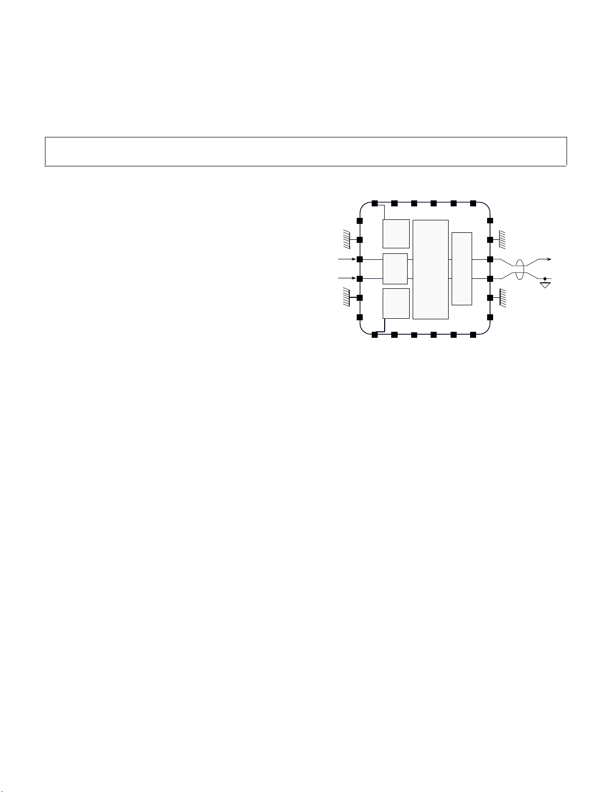
RF I/P
RF input, 50Ω
Three cascaded sections are used. The 50-Ω input system converts the
applied voltage to a pair of differential currents with high linearity and
good common rejection if driven by a single-sided source. The signal
currents are then applied to a proprietary voltage-controlled attenuator,
which provides precise definition of the overall gain, under the control
of the Linear-in-dB interface. Pin GAIN accepts a voltage from 0 V at
minimum gain to 1.4 V at full gain. The scaling factor is 20 mV/dB.
Optional external control of the input-stage and/or output-stage biasing
is provided using pins IPBS and OPBS respectively.
The output of the high-accuracy wideband attenuator is applied to a
differential trans-impedance output stage. Higher output power is
attainable at the lower operating frequencies by raising the supply
voltage to 6 V. When powered-down by a logic LO input on the ENBL
pin, the current consumption is < TBD µA.
The ADL5330 is available in a 24-lead (4 x 4mm) CSP package and is
specified for operation from ambient temperatures of −40°C to +85°C.
GAIN
VPS1
COM1
INHI
INLO
COM1
VPS1
VREF
ENBL VPS2
GAIN
CONTROL
Input
gm
Stage
BIAS
&
VREF
IPBS
Continuously
Variable
Attenuator
VPS2VPS2
COM2
O/P
(TZ)
Stage
VPS2
VPS2
COM2
OPHI
OPLO
COM2
VPS2
COM2COM2OPBS
Figure 1. Functional Block Diagram
RF to PA
BALUN
Rev. PrK
Information furnished by Analog Devices is believed to be accurate and
reliable. However, no responsibility is assumed by Analog Devices for its use;
nor for any infringements of patents or other rights of third parties which may
result from its use. No license is granted by implication or otherwise under
any patent or patent rights of Analog Devices.
Multiple Patents Pending
One Technology Way, P.O. Box 9106, Norwood, MA 02062-9106 U.S.A.
Tel: 781/329-4700 World Wide Web Site: http://www.analog.com
Fax: 781/326-8703 ©2004 Analog Devices, Inc. All Rights Reserved
Page 2

Preliminary Technical Data ADL5330
ADL5330 SPECIFICATIONS
Table 1. VS = 5 V; TA = 25°C; 800 MHz < f < 2.2GHz.1:1 balun at input and output for single-ended 50 Ω match
Parameter Conditions Min Typ Max Unit
General
Usable Frequency Range 0.001 3 GHz
Nominal Input Impedance via 1:1 Single-Sided to Differential Balun 50
Nominal Output Impedance via 1:1 Differential to Single-Sided Balun 50
100 MHz
Gain Control Span +/-3 dB Gain Law Conformance 58 dB
Max Gain V
Min Gain V
Gain Control Slope 21
Input Compression Point V
Output Compression Point - P1dB V
Third-Order Intercept - OIP3 V
900 MHz
Gain Control Span +/-3 dB Gain Law Conformance 52 dB
Max Gain V
Min Gain V
Gain Control Slope 20
Input Compression Point V
Output Compression Point - P1dB V
Third-Order Intercept - OIP3 V
Output Noise Floor 20 MHz Carrier Offset, V
1900 MHz
Gain Control Span +/-3 dB Gain Law Conformance 47 dB
Max Gain V
Min Gain V
Gain Control Slope 18
Input Compression Point V
Output Compression Point - P1dB V
Third-Order Intercept - OIP3 V
Output Noise Floor 20 MHz Carrier Offset, V
2200 MHz
Gain Control Span +/-3 dB Gain Law Conformance 48 dB
Max Gain V
Min Gain V
Gain Control Slope 17
Input Compression Point V
Output Compression Point - P1dB V
Third-Order Intercept - OIP3 V
GAIN CONTROL INPUT
Gain Control Voltage Range 0
Incremental Input Resistance Pin GAIN to COM1 TBD
Full-Scale Response Time V
POWER SUPPLIES
Voltage 4.75
Current, Nominal Active V
V
Current, Disabled
Ω
Ω
= 1.4 V +23 dB
GAIN
= 0.1 V
GAIN
-35
dB
mV/dB
= 1.3 V +2 dBm
GAIN
= 1.3 V +22 dBm
GAIN
= 1.3 V +36 dBm
GAIN
= 1.4 V 22 dB
GAIN
= 0.1 V -34 dB
GAIN
mV/dB
= 1.3 V +3 dBm
GAIN
= 1.3 V +22 dBm
GAIN
= 1.3 V +31 dBm
GAIN
GAIN
= 1.3 V,
-144 dBm/Hz
Pout = -2 dBm
= 1.4 V 19 dB
GAIN
= 0.5 V -27 dB
GAIN
mV/dB
= 1.3 V +1 dBm
GAIN
= 1.3 V +17 dBm
GAIN
= 1.3 V +24 dBm
GAIN
GAIN
= 1.3 V,
-148 dBm/Hz
Pout = -7 dBm
= 1.4 V 17 dB
GAIN
= 0.5 V -31 dB
GAIN
mV/dB
= 1.3 V +1 dBm
GAIN
= 1.3 V +14 dBm
GAIN
= 1.3 V +20 dBm
GAIN
Pin GAIN
1.4 V
0 - 1.6V, to within 0.25 dB of final gain
GN
Pins VPS1, VPS2, COM1, COM2, ENBL
= 0 V
GN
= 1.4 V 240 mA
GN
ENBL = LO
TBD TBD
500
5
6
TBD mA
MΩ
ns
V
µA
REV. PrK | Page 2 of 5
Page 3

Preliminary Technical Data ADL5330
Table 2. Pin Function Description
Pin Name Description
1,6
2,5
3, 4
7
8
9
10,11,12,14,
17
13,18,19,20,
21,22
15
16
23
24
VPS1
COM1
INHI,INLO
VREF
IPBS
OPBS
COM2
VPS2
OPLO
OPHI
ENBL
GAIN
J1
Enable
J2
Gain
Positive Supply for input stage. Nominally equal to 5 V
Common for input stage
Differential inputs
Voltage reference output of 1.5 volt s
Input bias, normally no connection. This function is subject to change. PCB
designs should include the possibility to connect a capacitor between Pin 8 and
Pin 9.
Output bias, normally no connection. This function is subject to change. PCB
designs should include the possibility to connect a capacitor between Pin 8 and
Pin 9.
Common for output stage
Positive Supply for output stage. Nominally equal to 5 V
Low side of differential output, bias to VP with RF chokes
High side of differential output, bias to VP with RF chokes
Device enable, apply logic high for normal operation. Enable Threshold = 1.6 V
Gain-control voltage input. Nominal Range 0 to 1.4 V.
VPOS
VPGND
R1
0
SW1
R3
0
R13
10k
C2
0.1 uF
R2
0
C1
100 pF
VPOSVPOS
C14
0.1 uF
R12
0
C13
100 pF
50 ohm microstrip
Input
VREF
IPBS
OPBS
C8
0.1 uF
VPOS
VPOS
T1
C3
0.1 uF
J3
25 ohm microstrip
(both sidesof caps)
J4
J5
J6
R5
0
C5
100 pF
C6
100 pF
R4
0
C7
100 pF
C4
100 pF
R8
0
R7
0
R9
0
R14
open
GAIN
VPS1
COM1
INHI
INLO
COM1
VPS1
VREF
R10
1nF
R15
open
R11
1nF
L
B
N
E
ADL5330
S
B
P
I
2
2
2
VPS2
S
S
S
P
P
P
VPS2
V
V
V
COM2
OPHI
OPLO
COM2
2
2
S
B
P
O
VPS2
M
M
O
C
O
C
COM2
C10
100 pF
L1
120 nH
C11
100 pF
25 ohm microstrip
R60C9
Figure 2. ADL5330 Evaluation Board Schematic
L2
120 nH
T2
C12 100 pF
0.1 uF
50 ohmmicrostrip
J7
Output
VPOS
REV. PrK | Page 3 of 5
Page 4

Preliminary Technical Data ADL5330
p
Typical Performance Characteristics
.
40
20.00
.
50
30
20
10
0
Gain - dB
-10
-20
-30
Gain 100 MHz
Gain 900 MHz
Gain 1900 MHz
2200 MHz
Error 100 MHz
Gain Error 900 MHz
Error 1900
Error 2200 MHz
-40
0 0.2 0.4 0.6 0.8 1 1.2 1.4 1.6
Vgain - Volts
15.00
10.00
5.00
0.00
-5.00
-10.00
-15.00
-20.00
40
30
20
100 MHz
10
OIP3
900 MHz
Error - dB
1900 MHz
0
2200 MHz
-10
-20
-30
0 0.2 0.4 0.6 0.8 1 1.2 1.4 1.6
Vgain - V
Figure 3. Gain and Gain Law Conformance vs. Vgain Figure 5. OIP3 vs. Gain
5
4
3
2
1
100 MHz
0
900 MHz
1900 MHz
-1
2200 MHz
Input Referred P1dB - dB
-2
-3
-4
-5
0 0.2 0.4 0.6 0.8 1 1.2 1.4 1.6
Vgain - V
30
20
10
0
100Mhz
-10
Output P1dB - dBm
-20
-30
-40
0 0.2 0.4 0.6 0.8 1 1.2 1.4 1.6
Vgain - V
900Mhz
1900Mhz
2200Mhz
Figure 4. Input Referred Compression Point vs. Gain Figure 7. Output Referred Compression Point vs. Gain
10.00
0.00
-10.00
-20.00
-30.00
Ou tp u t P o w e r - d B m
-40.00
-50.00
-60.00
0.00 0.20 0.40 0.60 0.80 1.00 1.20 1.40 1.60
Pout vs. Vin
Noise - 20 MHz offset
VGAIN
Figure 8. Pout and Noise Floor vs. Gain, 900 MHz. Pin = 21 dBm
-90.00
-100.00
-110.00
-120.00
-130.00
-140.00
-150.00
-160.00
0.00
-10.00
-20.00
.
Noise - 20 MHz Carrier Offset - dBm/Hz
ut Power - dB m
Out
-30.00
-40.00
-50.00
-60.00
Pout vs. Vin
Noise - 20 MHz
offset
0.00 0.20 0.40 0.60 0.80 1.00 1.20 1.40 1.60
VGAIN
Figure 8. Pout and Noise Floor vs. Gain 1.9 GHz. Pin = -22
dBm
-100.00
-110.00
-120.00
-130.00
-140.00
-150.00
-160.00
.
Noise - 20 MHz Carrier Offset - dBm /Hz
REV. PrK | Page 4 of 5
Page 5

Preliminary Technical Data ADL5330
PR05134-0-12/04(PrK)
OUTLINE DIMENSIONS
REV. PrK | Page 5 of 5
 Loading...