

Page 1
100 MHz to 4000 MHz
Data Sheet
FEATURES
Operating frequency from 100 MHz to 4000 MHz
Digitally controlled VGA with serial and parallel interfaces
6-bit, 0.5 dB digital step attenuator
31.5 dB gain control range with ±0.25 dB step accuracy
Gain Block Amplifier 1
Gain: 19.2 dB at 2140 MHz
OIP3: 40.2 dBm at 2140 MHz
P1dB: 19.8 dBm at 2140 MHz
Noise figure: 2.9 dB at 2140 MHz
¼ W Driver Amplifier 2
Gain: 14.2 dB at 2140 MHz
OIP3: 41.1 dBm at 2140 MHz
P1dB: 26.0 dBm at 2140 MHz
Noise figure: 3.7 dB at 2140 MHz
Gain block, DSA, or ¼ W driver amplifier can be first
Low quiescent current of 175 mA
The companion
APPLICATIONS
Wireless infrastructure
Automated test equipment
RF/IF gain control
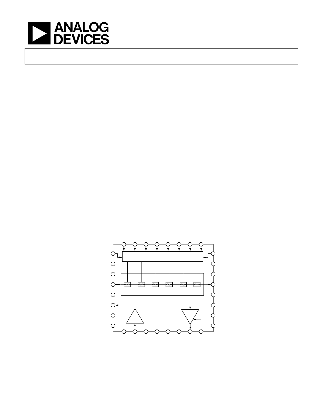
ADL5240 integrates a gain block with DSA
RF/IF Digitally Controlled VGA
ADL5243
GENERAL DESCRIPTION
The ADL5243 is a high performance, digitally controlled
variable gain amplifier operating from 100 MHz to 4000 MHz.
The VGA integrates two high performance amplifiers and a
digital step attenuator (DSA). Amplifier 1 (AMP1) is an
internally matched gain block amplifier with 20 dB gain, and
Amplifier 2 (AMP2) is a broadband ¼ W driver amplifier. The
DSA is 6-bit with a 31.5 dB gain control range, 0.5 dB steps, and
±0.25 dB step accuracy. The attenuation of the DSA can be
controlled using a serial or parallel interface.
The gain block and DSA are internally matched to 50 Ω at their
inputs and outputs, and all three internal devices are separately
biased. The separate bias allows all or part of the ADL5243 to be
used, which allows for easy reuse throughout a design. The
pinout of the ADL5243 also enables the gain block, DSA, or
¼ W driver amplifier to be first, giving the VGA maximum
flexibility in a signal chain.
The ADL5243 consumes 175 mA and operates off a single
supply ranging from 4.75 V to 5.25 V. The VGA is packaged in a
thermally efficient, 5 mm × 5 mm, 32-lead LFCSP and is fully
specified for operation from −40°C to +85°C. A fully populated
evaluation board is available.
FUNCTIONAL BLOCK DIAGRAM
SEL31D0/CLK30D1/DATA29D2/LE28D327D426D525D6
32
1
VDD
2
NC
3
NC
4
DSAIN
NC
AMP1OUT/VCC
NC
NC
Rev. A
Information furnished by Analog Devices is believed to be accurate and reliable. However, no
responsibility is assumed by Analog Devices for its use, nor for any infringements of patents or other
rights of third parties that may result from its use. Specifications subject to change without notice. No
license is granted by implication or otherwise under any patent or patent rights of Analog Devices.
Trademarks and registered trademarks are the property of their respective owners.
0.5dB 1dB 2dB 4dB 8dB 16dB
5
6
7
8
9NC10
SERIAL/PARAL LEL INT ERFACE
AMP1
11NC12NC13NC14NC15
AMP1IN
ADL5243
Figure 1.
24
VDD
23
NC
22
NC
21
DSAOUT
20
NC
19
AMP2IN
AMP2
AMP2OUT/VCC2
One Technology Way, P.O. Box 9106, Norwood, MA 02062-9106, U.S.A.
Tel: 781.329.4700 www.analog.com
Fax: 781.461.3113 ©2011 Analog Devices, Inc. All rights reserved.
18
NC
17
NC
16
VBIAS
09431-001
Page 2

ADL5243 Data Sheet
TABLE OF CONTENTS
Features.............................................................................................. 1
General Description ......................................................................... 1
Functional Block Diagram .............................................................. 1
Revision History ............................................................................... 2
Specifications..................................................................................... 3
Absolute Maximum Ratings............................................................ 9
ESD Caution.................................................................................. 9
Pin Configuration and Function Descriptions........................... 10
Typical Performance Characteristics ........................................... 11
Applications Information .............................................................. 20
REVISION HISTORY
8/11—Rev. 0 to Rev. A
Changes to Features Section............................................................ 1
7/11—Revision 0: Initial Version
Basic Layout Connections......................................................... 20
SPI Timing................................................................................... 21
ADL5243 Amplifier 2 Matching .............................................. 23
ADL5243 Loop Performance.................................................... 26
Thermal Considerations............................................................ 26
Soldering Information and Recommended PCB
Land Pattern................................................................................ 26
Evaluation Board............................................................................ 27
Outline Dimensions....................................................................... 30
Ordering Guide .......................................................................... 30
Rev. A | Page 2 of 32
Page 3

Data Sheet ADL5243
SPECIFICATIONS
VDD = 5V, VCC = 5V, VCC2 = 5V, TA = 25oC.
Table 1.
Parameter Conditions Min Typ Max Unit
OVERALL FUNCTION
Frequency Range 100 4000 MHz
AMPLIFIER 1 FREQUENCY = 150 MHz Using the AMP1IN and AMP1OUT pins
Gain 18.2 dB
vs. Frequency ±50 MHz ±0.97 dB
vs. Temperature −40°C ≤ TA ≤ +85°C ±0.07 dB
vs. Supply 4.75 V to 5.25 V ±0.03 dB
Input Return Loss S11 −10.4 dB
Output Return Loss S22 −8.2 dB
Output 1 dB Compression Point 18.4 dBm
Output Third-Order Intercept ∆f = 1 MHz, P
Noise Figure 2.8 dB
AMPLIFIER 1 FREQUENCY = 450 MHz Using the AMP1IN and AMP1OUT pins
Gain 20.6 dB
vs. Frequency ±50 MHz ±0.10 dB
vs. Temperature −40°C ≤ TA ≤ +85°C ±0.36 dB
vs. Supply 4.75 V to 5.25 V ±0.01 dB
Input Return Loss S11 −17.8 dB
Output Return Loss S22 −16.5 dB
Output 1 dB Compression Point 19.5 dBm
Output Third-Order Intercept ∆f = 1 MHz, P
Noise Figure 2.8 dB
AMPLIFIER 1 FREQUENCY = 748 MHz Using the AMP1IN and AMP1OUT pins
Gain 20.8 dB
vs. Frequency ±50 MHz ±0.02 dB
vs. Temperature −40°C ≤ TA ≤ +85°C ±0.32 dB
vs. Supply 4.75 V to 5.25 V ±0.01 dB
Input Return Loss S11 −22.0 dB
Output Return Loss S22 −21.6 dB
Output 1 dB Compression Point 19.6 dBm
Output Third-Order Intercept ∆f = 1 MHz, P
Noise Figure 2.7 dB
AMPLIFIER 1 FREQUENCY = 943 MHz Using the AMP1IN and AMP1OUT pins
Gain 19.0 20.3 22.0 dB
vs. Frequency ±18 MHz ±0.01 dB
vs. Temperature −40°C ≤ TA ≤ +85°C ±0.28 dB
vs. Supply 4.75 V to 5.25 V ±0.02 dB
Input Return Loss S11 −24.0 dB
Output Return Loss S22 −21.5 dB
Output 1 dB Compression Point 18.5 19.9 dBm
Output Third-Order Intercept ∆f = 1 MHz, P
Noise Figure 2.7 dB
= 3 dBm/tone 29.5 dBm
OUT
= 3 dBm/tone 38.4 dBm
OUT
= 3 dBm/tone 39.6 dBm
OUT
= 3 dBm/tone 40.4 dBm
OUT
Rev. A | Page 3 of 32
Page 4

ADL5243 Data Sheet
Parameter Conditions Min Typ Max Unit
AMPLIFIER 1 FREQUENCY = 1960 MHz Using the AMP1IN and AMP1OUT pins
Gain 19.5 dB
vs. Frequency ±30 MHz ±0.02 dB
vs. Temperature −40°C ≤ TA ≤ +85°C ±0.26 dB
vs. Supply 4.75 V to 5.25 V ±0.04 dB
Input Return Loss S11 −13.5 dB
Output Return Loss S22 −12.4 dB
Output 1 dB Compression Point 19.6 dBm
Output Third-Order Intercept ∆f = 1 MHz, P
Noise Figure 2.9 dB
AMPLIFIER 1 FREQUENCY = 2140 MHz Using the AMP1IN and AMP1OUT pins
Gain 17.5 19.2 21.5 dB
vs. Frequency ±30 MHz ±0.02 dB
vs. Temperature −40°C ≤ TA ≤ +85°C ±0.26 dB
vs. Supply 4.75 V to 5.25 V ±0.05 dB
Input Return Loss S11 −13.3 dB
Output Return Loss S22 −12.2 dB
Output 1 dB Compression Point 17.5 19.8 dBm
Output Third-Order Intercept ∆f = 1 MHz, P
Noise Figure 2.9 dB
AMPLIFIER 1 FREQUENCY = 2630 MHz Using the AMP1IN and AMP1OUT pins
Gain 17.5 19.0 21.5 dB
vs. Frequency ±60 MHz ±0.03 dB
vs. Temperature −40°C ≤ TA ≤ +85°C ±0.22 dB
vs. Supply 4.75 V to 5.25 V ±0.05 dB
Input Return Loss S11 −17.3 dB
Output Return Loss S22 −12.3 dB
Output 1 dB Compression Point 17.5 19.5 dBm
Output Third-Order Intercept ∆f = 1 MHz, P
Noise Figure 2.9 dB
AMPLIFIER 1 FREQUENCY = 3600 MHz Using the AMP1IN and AMP1OUT pins
Gain 18.0 dB
vs. Frequency ±100 MHz ±0.10 dB
vs. Temperature −40°C ≤ TA ≤ +85°C ±0.05 dB
vs. Supply 4.75 V to 5.25 V ±0.12 dB
Input Return Loss S11 −30.7 dB
Output Return Loss S22 −9.0 dB
Output 1 dB Compression Point 18.0 dBm
Output Third-Order Intercept ∆f = 1 MHz, P
Noise Figure 3.3 dB
AMPLIFIER 2 FREQUENCY = 748 MHz Using the AMP2IN and AMP2OUT pins
Gain 17.5 dB
vs. Frequency ±50 MHz ±0.14 dB
Input Return Loss S11 −12.7 dB
Output Return Loss S22 −8.6 dB
Output 1 dB Compression Point 24.7 dBm
Output Third-Order Intercept ∆f = 1 MHz, P
Noise Figure 5.6 dB
= 3 dBm/tone 40.4 dBm
OUT
= 3 dBm/tone 40.2 dBm
OUT
= 3 dBm/tone 39.5 dBm
OUT
= 3 dBm/tone 34.6 dBm
OUT
= 5 dBm/tone 41.5 dBm
OUT
Rev. A | Page 4 of 32
Page 5

Data Sheet ADL5243
Parameter Conditions Min Typ Max Unit
AMPLIFIER 2 FREQUENCY = 943 MHz Using the AMP2IN and AMP2OUT pins
Gain 16.5 dB
vs. Frequency ±18 MHz ±0.05 dB
vs. Temperature −40°C ≤ TA ≤ +85°C ±0.39 dB
vs. Supply 4.75 V to 5.25 V ±0.10 dB
Input Return Loss S11 −11.2 dB
Output Return Loss S22 −8.1 dB
Output 1 dB Compression Point 25.0 dBm
Output Third-Order Intercept ∆f = 1 MHz, P
Noise Figure 5.3 dB
AMPLIFIER 2 FREQUENCY = 2140 MHz Using the AMP2IN and AMP2OUT pins
Gain 13.0 14.2 15.5 dB
vs. Frequency ±30 MHz ±0.03 dB
vs. Temperature −40°C ≤ TA ≤ +85°C ±0.50 dB
vs. Supply 4.75 V to 5.25 V ±0.09 dB
Input Return Loss S11 −10.7 dB
Output Return Loss S22 −8.1 dB
Output 1 dB Compression Point 26.0 dBm
Output Third-Order Intercept ∆f = 1 MHz, P
Noise Figure 3.7 dB
AMPLIFIER 2 FREQUENCY = 2630 MHz Using the AMP2IN and AMP2OUT pins
Gain 13.0 dB
vs. Frequency ±60 MHz ±0.13 dB
vs. Temperature −40°C ≤ TA ≤ +85°C ±0.56 dB
vs. Supply 4.75 V to 5.25 V ±0.09 dB
Input Return Loss S11 −9.4 dB
Output Return Loss S22 −8.3 dB
Output 1 dB Compression Point 24.5 dBm
Output Third-Order Intercept ∆f = 1 MHz, P
Noise Figure 4.1 dB
DSA FREQUENCY = 150 MHz
Using the DSAIN and DSAOUT pins, minimum
attenuation
Insertion Loss −1.5 dB
vs. Frequency ±50 MHz ±0.12 dB
vs. Temperature −40°C ≤ TA ≤ +85°C ±0.10 dB
Attenuation Range Between maximum and minimum attenuation states 28.8 dB
Attenuation Step Error All attenuation states ±0.18 dB
Attenuation Absolute Error All attenuation states ±1.35 dB
Input Return Loss −13.5 dB
Output Return Loss −13.3 dB
Input Third-Order Intercept ∆f = 1 MHz, P
= 5 dBm/tone 43.3 dBm
OUT
= 5 dBm/tone 41.1 dBm
OUT
= 5 dBm/tone 40.4 dBm
OUT
= 5 dBm/tone 45.2 dBm
OUT
Rev. A | Page 5 of 32
Page 6

ADL5243 Data Sheet
Parameter Conditions Min Typ Max Unit
DSA FREQUENCY = 450 MHz
Using the DSAIN and DSAOUT pins, minimum
attenuation
Insertion Loss −1.4 dB
vs. Frequency ±50 MHz ±0.02 dB
vs. Temperature −40°C ≤ TA ≤ +85°C ±0.12 dB
Attenuation Range Between maximum and minimum attenuation states 30.7 dB
Attenuation Step Error All attenuation states ±0.14 dB
Attenuation Absolute Error All attenuation states ±0.39 dB
Input Return Loss −17.7 dB
Output Return Loss −17.4 dB
Input Third-Order Intercept ∆f = 1 MHz, P
DSA FREQUENCY = 748 MHz
Using the DSAIN and DSAOUT pins, minimum
= 5 dBm/tone 41.2 dBm
OUT
attenuation
Insertion Loss −1.5 dB
vs. Frequency ±50 MHz ±0.02 dB
vs. Temperature −40°C ≤ TA ≤ +85°C ±0.12 dB
Attenuation Range Between maximum and minimum attenuation states 30.9 dB
Attenuation Step Error All attenuation states ±0.15 dB
Attenuation Absolute Error All attenuation states ±0.30 dB
Input Return Loss −17.1 dB
Output Return Loss −17.1 dB
Input Third-Order Intercept ∆f = 1 MHz, P
DSA FREQUENCY = 943 MHz
Using the DSAIN and DSAOUT pins, minimum
= 5 dBm/tone 40.4 dBm
OUT
attenuation
Insertion Loss −1.6 dB
vs. Frequency ±18 MHz ±0.01 dB
vs. Temperature −40°C ≤ TA ≤ +85°C ±0.13 dB
Attenuation Range Between maximum and minimum attenuation states 30.9 dB
Attenuation Step Error All attenuation states ±0.15 dB
Attenuation Absolute Error All attenuation states ±0.28 dB
Input Return Loss −16.0 dB
Output Return Loss −15.9 dB
Input 1 dB Compression Point 30.5 dBm
Input Third-Order Intercept ∆f = 1 MHz, P
DSA FREQUENCY = 1960 MHz
Using the DSAIN and DSAOUT pins, minimum
= 5 dBm/tone 48.3 dBm
OUT
attenuation
Insertion Loss −2.5 dB
vs. Frequency ±30 MHz ±0.04 dB
vs. Temperature −40°C ≤ TA ≤ +85°C ±0.18 dB
Attenuation Range Between maximum and minimum attenuation states 30.8 dB
Attenuation Step Error All attenuation states ±0.15 dB
Attenuation Absolute Error All attenuation states ±0.35 dB
Input Return Loss −10.3 dB
Output Return Loss −9.6 dB
Input 1 dB Compression Point 31.5 dBm
Input Third-Order Intercept ∆f = 1 MHz, P
= 5 dBm/tone 44.7 dBm
OUT
Rev. A | Page 6 of 32
Page 7

Data Sheet ADL5243
Parameter Conditions Min Typ Max Unit
DSA FREQUENCY = 2140 MHz
Using the DSAIN and DSAOUT pins, minimum
attenuation
Insertion Loss −2.6 dB
vs. Frequency ±30 MHz ±0.02 dB
vs. Temperature −40°C ≤ TA ≤ +85°C ±0.19 dB
Attenuation Range Between maximum and minimum attenuation states 30.9 dB
Attenuation Step Error All attenuation states ±0.13 dB
Attenuation Absolute Error All attenuation states ±0.32 dB
Input Return Loss −9.8 dB
Output Return Loss −9.3 dB
Input 1 dB Compression Point 31.5 dBm
Input Third-Order Intercept ∆f = 1 MHz, P
DSA FREQUENCY = 2630 MHz
Using the DSAIN and DSAOUT pins, minimum
= 5 dBm/tone 44.6 dBm
OUT
attenuation
Insertion Loss −2.8 dB
vs. Frequency ±60 MHz ±0.02 dB
vs. Temperature −40°C ≤ TA ≤ +85°C ±0.21 dB
Attenuation Range Between maximum and minimum attenuation states 31.2 dB
Attenuation Step Error All attenuation states ±0.18 dB
Attenuation Absolute Error All attenuation states ±0.24 dB
Input Return Loss −10.0 dB
Output Return Loss −9.6 dB
Input 1 dB Compression Point 31.5 dBm
Input Third-Order Intercept ∆f = 1 MHz, P
DSA FREQUENCY = 3600 MHz
Using the DSAIN and DSAOUT pins, minimum
= 5 dBm/tone 43.8 dBm
OUT
attenuation
Insertion Loss −3.0 dB
vs. Frequency ±100 MHz ±0.02 dB
vs. Temperature −40°C ≤ TA ≤ +85°C ±0.23 dB
Attenuation Range Between maximum and minimum attenuation states 31.7 dB
Attenuation Step Error All attenuation states ±0.38 dB
Attenuation Absolute Error All attenuation states ±0.18 dB
Input Return Loss −12.3 dB
Output Return Loss −11.7 dB
Input 1 dB Compression Point 31.0 dBm
Input Third-Order Intercept ∆f = 1 MHz, P
= 5 dBm/tone 42.2 dBm
OUT
DSA Gain Settling Using the DSAIN and DSAOUT pins
Minimum Attenuation to Maximum
36 ns
Attenuation
Maximum Attenuation to Minimum
36 ns
Attenuation
LOOP FREQUENCY = 943 MHz AMP1–DSA–AMP2, DSA at minimum attenuation
Gain 34.0 dB
vs. Frequency ±18 MHz ±0.10 dB
Gain Range Between maximum and minimum attenuation states 29.3 dB
Input Return Loss S11 −14.2 dB
Output Return Loss S22 −10.1 dB
Output 1 dB Compression Point 25.1 dBm
Output Third-Order Intercept ∆f = 1 MHz, P
= 5 dBm/tone 42.8 dBm
OUT
Noise Figure 2.9 dB
Rev. A | Page 7 of 32
Page 8

ADL5243 Data Sheet
Parameter Conditions Min Typ Max Unit
LOOP FREQUENCY = 2140 MHz AMP1 – DSA – AMP2, DSA at minimum attenuation
Gain 31.3 dB
vs. Frequency ±30 MHz ±0.03 dB
Gain Range Between maximum and minimum attenuation states 32.5 dB
Input Return Loss S11 −9.3 dB
Output Return Loss S22 −5.4 dB
Output 1 dB Compression Point 25.3 dBm
Output Third-Order Intercept ∆f = 1 MHz, P
Noise Figure 3.1 dB
LOOP FREQUENCY = 2630 MHz AMP1 – DSA – AMP2, DSA at minimum attenuation
Gain 29.5 dB
vs. Frequency ±60 MHz ±0.56 dB
Gain Range Between maximum and minimum attenuation states 30.0 dB
Input Return Loss S11 −12.6 dB
Output Return Loss S22 −5.8 dB
Output 1 dB Compression Point 24.6 dBm
Output Third-Order Intercept ∆f = 1 MHz, P
Noise Figure 3.1 dB
POWER SUPPLIES
Voltage 4.75 5.0 5.25 V
Supply Current AMP1 89 120 mA
AMP2 86 120 mA
DSA 0.5 mA
= 5 dBm/tone 40.0 dBm
OUT
= 5 dBm/tone 39.3 dBm
OUT
Rev. A | Page 8 of 32
Page 9
Data Sheet ADL5243
ABSOLUTE MAXIMUM RATINGS
Table 2.
Parameter Rating
Supply Voltage (VDD, VCC, VCC2) 6.5 V
Input Power
AMP1IN 16 dBm
AMP2IN (50 Ω Impedance)
DSAIN 30 dBm
Internal Power Dissipation 1.0 W
θJA (Exposed Paddle Soldered Down) 34.8°C/W
θJC (Exposed Paddle) 6.2°C/W
Maximum Junction Temperature 150°C
Lead Temperature (Soldering, 60 sec) 240°C
Operating Temperature Range −40°C to +85°C
Storage Temperature Range −65°C to +150°C
Stresses above those listed under Absolute Maximum Ratings
may cause permanent damage to the device. This is a stress
rating only; functional operation of the device at these or any
other conditions above those indicated in the operational
section of this specification is not implied. Exposure to absolute
maximum rating conditions for extended periods may affect
device reliability.
20 dBm
ESD CAUTION
Rev. A | Page 9 of 32
Page 10
ADL5243 Data Sheet
PIN CONFIGURATION AND FUNCTION DESCRIPTIONS
D3
SEL
32
D4
D1/DATA
D2/LE
D5
D0/CLK
31
30
D6
29
28
27
26
25
1VDD
PIN 1
2NC
INDICATOR
3NC
ADL5243
4DSAIN
5NC
TOP VIEW
(Not to Scale)
6AMP1OUT/VCC
7NC
8NC
9
11
10
12
13
NC
NC
NC
NC
AMP1IN
NOTES
1. NC = NO CONNECT . DO NOT CONNECT TO T HIS PIN.
2. THE EXPOSED PAD MUST BE CONNECTED TO GROUND.
24 VDD
23 NC
22 NC
21 DSAOUT
20 NC
19 AMP2IN
18 NC
17 NC
14
15
16
NC
VBIAS
AMP2OUT/VCC2
09431-002
Figure 2. Pin Configuration
Table 3. Pin Function Descriptions
Pin No. Mnemonic Description
1, 24 VDD Supply Voltage for DSA. Connect this pin to a 5 V supply.
2, 3, 5, 7, 8, 9, 11, 12, 13, 14,
NC No Connect. Do not connect to this pin.
17, 18, 20, 22, 23
4 DSAIN RF Input to DSA.
6 AMP1OUT/VCC
RF Output from Amplifier 1/Supply Voltage for Amplifier 1. Bias to Gain Block
Amplifier 1 is provided through a choke to this pin when connected to VCC.
10 AMP1IN RF Input to Gain Block Amplifier 1.
15 AMP2OUT/VCC2
RF Output from Amplifier 2/Supply Voltage for Amplifier 2. Bias to Driver Amplifier 2 is
provided through a choke to this pin when connected to VCC2.
16 VBIAS Bias for Driver Amplifier 2.
19 AMP2IN RF Input to Amplifier 2.
21 DSAOUT RF Output from DSA.
25 D6 Data Bit in Parallel Mode (LSB). Connect to supply in serial mode.
26 D5 Data Bit in Parallel Mode. Connect to ground in serial mode.
27 D4 Data Bit in Parallel Mode. Connect to ground in serial mode.
28 D3 Data Bit in Parallel Mode. Connect to ground in serial mode.
29 D2/LE Data Bit in Parallel Mode/Latch Enable in Serial Mode.
30 D1/DATA Data Bit in Parallel Mode (MSB)/Data in Serial Mode.
31 D0/CLK
Connect this pin to ground in parallel mode. This pin functions as a clock in serial
mode.
32 SEL
Select Pin. Connect this pin to the supply for parallel mode operation; connect this pin
to ground for serial mode operation.
EPAD Exposed Paddle. The exposed paddle must be connected to ground.
Rev. A | Page 10 of 32
Page 11

Data Sheet ADL5243
TYPICAL PERFORMANCE CHARACTERISTICS
45
40
35
30
25
20
15
10
5
NOISE FIGURE, GAIN, P1dB, OIP3 (dB, dBm)
0
0 0.4 0.8 1.2 1.6 2. 0 2.4 2.8 3.2 3. 6
Figure 3. AMP1: Gain, P1dB, OIP3 at P
FREQUENCY (GHz)
= 3 dBm/Tone and Noise Figure vs.
OUT
OIP3
P1dB
GAIN
NF
Frequency
22.0
21.5
21.0
20.5
20.0
19.5
GAIN (dB)
19.0
18.5
18.0
17.5
17.0
0 0.4 0. 8 1.2 1.6 2.0 2.4 2.8 3.2 3. 6
–40°C
+25°C
+85°C
FREQUENCY (G Hz)
Figure 4. AMP1: Gain vs. Frequency and Temperature
0
–5
–10
–15
–20
–25
–30
–35
S-PARAMETERS (dB)
–40
–45
–50
0.1 0.5 0.9 1.3 1.7 2.1 2.5 2.9 3.3 3.7 4.1
FREQUENCY (G Hz)
S22
S11
S12
Figure 5. AMP1: Input Return Loss (S11), Output Return Loss (S22), and
Reverse Isolation (S12) vs. Frequency
09431-003
09431-004
09431-005
28
26
24
22
20
P1dB (dBm)
18
16
14
0 0.4 0.8 1.2 1.6 2. 0 2. 4 2.8 3.2 3. 6
+85°C
+25°C
–40°C
FREQUENCY (GHz)
45
40
35
30
25
OIP3 (dBm)
20
15
10
Figure 6. AMP1: OIP3 at Pout = 3 dBm/Tone and P1dB vs. Frequency and
Temperature
42
943MHz
NOISE FIGURE (dB)
OIP3 (dBm)
5.0
4.5
4.0
3.5
3.0
2.5
2.0
1.5
40
38
1960MHz
36
34
32
30
3600MHz
28
26
24
22
20
–4 1614121086420–2
Figure 7. AMP1: OIP3 vs. P
043.63.22.82.42.01.61.20.80.4
150MHz
P
PER TONE (d Bm)
OUT
+85°C
+25°C
–40°C
FREQUENCY (GHz)
2140MHz
2630MHz
and Frequency
OUT
450MHz
748MHz
09431-007
.0
Figure 8. AMP1: Noise Figure vs. Frequency and Temperature
09431-008
09431-006
Rev. A | Page 11 of 32
Page 12

ADL5243 Data Sheet
50
45
40
35
30
25
20
15
10
5
NOISE FIGURE, GAIN, P1dB, OIP3 (dB, dBm)
0
0.925 0.930 0.935 0.940 0.945 0.950 0.955 0.960 0.965
Figure 9. AMP2–943 MHz: Gain, P1dB, OIP3 at P
FREQUENCY (GHz)
= 5 dBm/Tone and Noise
OUT
Figure vs. Frequency
18.0
OIP3
P1dB
GAIN
NF
09431-009
27.0
26.5
26.0
25.5
P1dB (dBm)
25.0
24.5
24.0
0.925 0.930 0.935 0.940 0.945 0.950 0.955 0.960 0.965
Figure 12. AMP2–943 MHz: OIP3 at P
+85°C
+25°C
–40°C
FREQUENCY (GHz)
OUT
= 5 dBm/Tone and P1dB vs.
Frequency and Temperature
45
45
43
41
39
OIP3 (dBm)
37
35
33
09431-012
17.5
17.0
16.5
GAIN (dB)
16.0
15.5
15.0
0.925 0.930 0.935 0.940 0.945 0.950 0.955 0.960 0.965
–40°C
+25°C
+85°C
FREQUENCY (G Hz)
FREQUENCY (G Hz)
Figure 10. AMP2–943 MHz: Gain vs. Frequency and Temperature
0
–5
S22
–10
–15
–20
S-PARAMETERS (dB)
–25
–30
S11
S12
44
43
42
41
OIP3 (dBm)
40
39
38
37
09431-010
7.5
7.0
6.5
6.0
5.5
5.0
NOISE FIGURE (dB)
4.5
4.0
961MHz
925MHz
943MHz
–4 1816121086420–2
P
PER TONE (d Bm)
OUT
Figure 13. AMP2–943 MHz: OIP3 vs. P
+85°C
+25°C
–40°C
–40°C
14
and Frequency
OUT
09431-013
–35
0.80 0.85 0.90 0.95 1.00 1.05 1. 10
FREQUENCY (G Hz)
09431-011
Figure 11. AMP2–943 MHz: Input Return Loss (S11), Output Return Loss (S22,)
and Reverse Isolation (S12) vs. Frequency
Rev. A | Page 12 of 32
3.5
0.80 1.101.071.041.010.980.950.920.890.860.83
FREQUENCY (G Hz)
Figure 14. AMP2–943 MHz: Noise Figure vs. Frequency and Temperature
09431-014
Page 13

Data Sheet ADL5243
45
40
35
30
25
20
15
10
5
NOISE FIGURE, GAIN, P1dB, OIP3 (dB, dBm)
0
2.11 2.12 2.13 2.14 2.15 2.16 2.17
Figure 15. AMP2–2140 MHz: Gain, P1dB, OIP3 at P
OIP3
P1dB
GAIN
NF
FREQUENCY (G Hz)
= 5 dBm/Tone and
OUT
Noise Figure vs. Frequency
16.0
15.5
15.0
14.5
14.0
GAIN (dB)
13.5
13.0
12.5
12.0
2.11 2.12 2.13 2.14 2.15 2.16 2.17
–40°C
+25°C
+85°C
FREQUENCY ( GHz)
Figure 16. AMP2–2140 MHz: Gain vs. Frequency and Temperature
0
28.0
27.5
27.0
26.5
P1dB (dBm)
26.0
25.5
25.0
2.11 2.12 2.13 2.14 2.15 2.16 2.17
09431-015
Figure 18. AMP2–2140 MHz: OIP3 at P
+85°C
+25°C
–40°C
FREQUENCY ( GHz)
= 5 dBm/Tone and P1dB vs.
OUT
Frequency and Temperature
42
41
40
39
38
OIP3 (dBm)
37
36
35
34
–6 –4 –2 0 2 4 6 8 10 12 14 16 18 20 22
09431-016
Figure 19. AMP2–2140 MHz: OIP3 vs. P
5.5
2.11GHz
2.17GHz
2.14GHz
P
PER TONE (dBm)
OUT
and Frequency
OUT
43
41
39
37
OIP3 (dBm)
35
33
31
09431-019
09431-018
–5
–10
–15
–20
S-PARAMETERS (dB)
–25
–30
2.00 2.05 2.10 2.15 2.20 2.25 2.30
S11
S22
S12
FREQUENCY (G Hz)
Figure 17. AMP2–2140 MHz: Input Return Loss (S11), Output Return Loss
(S22), and Reverse Isolation (S12) vs. Frequency
Rev. A | Page 13 of 32
5.0
4.5
4.0
3.5
NOISE FIGURE (dB)
3.0
2.5
2.0
2.00 2.302.272.242.212.182.152.122.092.062.03
09431-017
+85°C
+25°C
–40°C
FREQUENCY (G Hz)
09431-020
Figure 20. AMP2–2140 MHz: Noise Figure vs. Frequency and Temperature
Page 14

ADL5243 Data Sheet
45
40
35
30
25
20
15
10
5
NOISE FIGURE, GAIN, P1dB, OIP3 (dB, dBm)
0
2.57 2.59 2.61 2.63 2.65 2.67 2.69
Figure 21. AMP2–2630 MHz: Gain, P1dB, OIP3 at P
OIP3
P1dB
GAIN
NF
FREQUENCY (GHz)
= 5 dBm/Tone and
OUT
Noise Figure vs. Frequency
15.0
14.5
GAIN (dB)
14.0
13.5
13.0
12.5
12.0
11.5
11.0
–40°C
+25°C
+85°C
2.57 2.59 2.61 2.63 2.65 2.67 2.69
FREQUENCY (GHz)
Figure 22. AMP2–2630 MHz: Gain vs. Frequency and Temperature
0
28.0
27.5
27.0
26.5
26.0
25.5
25.0
P1dB (dBm)
24.5
24.0
23.5
23.0
2.57 2.59 2.61 2.63 2.65 2.67 2.69
09431-021
Figure 24. AMP2–2630 MHz: OIP3 at P
+85°C
+25°C
–40°C
FREQUENCY ( GHz)
OUT
= 5 dBm/Tone and P1dB vs.
Frequency and Temperature
42
2.69GHz
41
40
39
38
37
36
35
OIP3 (dBm)
34
33
32
31
30
–6 –4 –2 0 2 4 6 8 10 12 14 16 18 20 22
09431-022
2.57GHz
P
PER TONE (dBm)
OUT
Figure 25. AMP2–2630 MHz: OIP3 vs. P
6.0
2.63GHz
and Frequency
OUT
42.0
41.5
41.0
40.5
40.0
39.5
39.0
38.5
38.0
37.5
37.0
OIP3 (dBm)
09431-025
09431-024
–5
–10
–15
–20
S-PARAMETERS (dB)
–25
–30
2.50 2.55 2.60 2.65 2.70 2.75 2. 80
S11
S22
S12
FREQUENCY (G Hz)
Figure 23. AMP2–2630 MHz: Input Return Loss (S11), Output Return Loss
(S22), and Reverse Isolation (S12) vs. Frequency
Rev. A | Page 14 of 32
5.5
5.0
4.5
4.0
3.5
NOISE FIGURE (dB)
3.0
2.5
2.0
2.50 2.802.772.742.712.682.652.622.592.562.53
09431-023
+85°C
+25°C
–40°C
FREQUENCY (GHz)
09431-026
Figure 26. AMP2–2630 MHz: Noise Figure vs. Frequency and Temperature
Page 15

Data Sheet ADL5243
–
0
–5
–10
–15
–20
–25
ATTENUATION (dB)
–30
–35
–40
0.1 4.13.73.32.92.52.11.71.30.90.5
31.5dB
FREQUENCY (G Hz)
Figure 27. DSA: Attenuation vs. Frequency
1
ATTENUATIO N (dB)
–6
–11
–16
–21
–26
–31
–36
0.1 4.13.73.32.92.52.11.71.30.90.5
4dB
8dB
16dB
31.5dB
FREQUENCY (GHz)
Figure 28. DSA: Attenuation vs. Frequency and Temperature
0.5
450MHz
748MHz
0.4
943MHz
0.3
0.2
0.1
0
–0.1
STEP ERROR (dB)
–0.2
–0.3
–0.4
–0.5
032282420161284
1960MHz
2140MHz
2630MHz
3600MHz
ATTENUATION (dB)
Figure 29. DSA: Step Error vs. Attenuation
0dB
0dB
+85°C
+25°C
–40°C
1.0
450MHz
748MHz
0.8
943MHz
0.6
0.4
0.2
0
–0.2
–0.4
ABSOLUTE ERRO R (dB)
–0.6
–0.8
–1.0
03282420161284
09431-027
1960MHz
2140MHz
2630MHz
3600MHz
ATTENUATION (dB)
2
09431-030
Figure 30. DSA: Absolute Error vs. Attenuation
0
–5
0dB
–10
–15
–20
INPUT RETURN LOSS (dB)
–25
–30
0.1 4.13.73.32.92.52.11.71.30.90. 5
09431-028
FREQUENCY (G Hz)
31.5dB
09431-031
Figure 31. DSA: Input Return Loss vs. Frequency, All States
0
–5
–10
–15
–20
OUTPUT RETURN LOSS (d B)
–25
–30
0.1 4.13.73.32.92.52.11.71.30.90.5
09431-029
0dB
FREQUENCY (G Hz)
31.5dB
09431-032
Figure 32. DSA: Output Return Loss vs. Frequency, All States
Rev. A | Page 15 of 32
Page 16

ADL5243 Data Sheet
36
35
34
33
IP1dB (dBm)
32
IIP3
IP1dB
50
45
40
35
IIP3 (dBm)
30
PHASE (Degrees)
150
100
–50
1960MHz
2140MHz
50
2630MHz
0
31
30
0.9 1. 2 1. 5 1. 8 2.1 2.4 2.7 3.0 3.3 3.6
FREQUENCY ( GHz)
25
20
Figure 33. DSA: Input P1dB and Input IP3 vs. Frequency, Minimum
Attenuation State
3
4
CH3 2.00VCH3 2.00V CH4 200mV M 10ns 10GS/ s
IT 1.0ps/pt
A CH3 1.24V
Figure 34. DSA: Gain Settling Time, 0 dB to 31.5 dB
3
4
CH3 2.00VCH3 2.00V CH4 200mV M 10ns 10GS/ s
IT 1.0ps/pt
A CH3 1.24V
Figure 35. DSA: Gain Settling Time, 31.5 dB to 0 dB
–100
–150
0 4 8 12 16 20 24 28 32
09431-033
943MHz
ATTENUATION (dB)
09431-036
Figure 36. DSA: Phase vs. Attenuation
50
45
40
35
30
25
20
15
10
5
NOISE FIGURE, GAIN, P1dB, OIP3 (dB, dBm)
0
09431-034
925 930 935 940 945 950 955 960 965
Figure 37. Loop–943 MHz: Gain, P1dB, OIP3 at P
OIP3
GAIN
P1dB
NF
FREQUENCY ( MHz)
= 5 dBm/Tone and Noise
OUT
09431-037
Figure vs. Frequency, Minimum Attenuation State
0
–10
–20
–30
–40
–50
–60
S-PARAMETERS (dB)
–70
–80
–90
09431-035
0.70 0.75 0.80 0.85 0.90 0.95 1.00 1.05 1.10
S22
S11
S12
FREQUENCY ( GHz)
09431-038
Figure 38. Loop–943 MHz: Input Return Loss (S11), Output Return Loss (S22),
and Reverse Isolation (S12) vs. Frequency, Minimum Attenuation State
Rev. A | Page 16 of 32
Page 17

Data Sheet ADL5243
46
44
42
40
38
OIP3 (dBm)
36
34
961MHz
925MHz
943MHz
42
41
40
39
38
OIP3 (dBm)
37
36
35
2.14GHz
2.11GHz
2.17GHz
32
4 6 8 10 12 14 16 18 20 22
Figure 39. Loop–943 MHz: OIP3 vs. P
P
PER TONE (dBm)
OUT
and Frequency, Minimum
OUT
Attenuation State
45
40
35
30
25
20
15
10
5
NOISE FIGURE, GAIN, P1dB, OIP3 (dB, dBm)
0
2.11 2.12 2.13 2.14 2.15 2.16 2.17
OIP3
GAIN
P1dB
NF
FREQUENCY (GHz)
Figure 40. Loop–2140 MHz: Gain, P1dB, OIP3 at P
Figure vs. Frequency, Minimum Attenuation State
5
0
–5
–10
–15
–20
–25
S-PARAMETERS (dB)
–30
–35
–40
–45
2.00 2.05 2.10 2.15 2.20 2.25 2.30
FREQUENCY ( GHz)
Figure 41. Loop
–
2140 MHz: Input Return Loss (S11), Output Return Loss
= 5 dBm/Tone and Noise
OUT
S22
S11
S12
34
13579111315171921
09431-039
Figure 42. Loop–2140 MHz: OIP3 vs. P
P
PER TONE (dBm)
OUT
and Frequency, Minimum
OUT
09431-042
Attenuation State
45
40
35
30
25
20
15
10
5
NOISE FIGURE, GAIN, P1dB, OIP3 (dB, dBm)
0
2.57 2.59 2.61 2.63 2.65 2.67 2.69
09431-040
Figure 43. Loop–2630 MHz: Gain, P1dB, OIP3 at P
OIP3
GAIN
P1dB
NF
FREQUENCY (GHz)
= 5 dBm/Tone and Noise
OUT
09431-043
Figure vs. Frequency, Minimum Attenuation State
5
0
–5
–10
–15
–20
–25
–30
S-PARAMETERS (dB)
–35
–40
–45
–50
2.50 2.55 2.60 2.65 2.70 2.75 2.80 2.85 2.90
09431-041
S22
S11
S12
FREQUENCY ( GHz)
09431-044
Figure 44. Loop–2630 MHz: Input Return Loss (S11), Output Return Loss
(S22), and Reverse Isolation (S12) vs. Frequency, Minimum Attenuation State
(S22), and Reverse Isolation (S12) vs. Frequency, Minimum Attenuation State
Rev. A | Page 17 of 32
Page 18

ADL5243 Data Sheet
42
41
40
39
38
37
OIP3 (dBm)
36
35
34
33
0 2 4 6 8 10121416 18
2.69GHz
P
Figure 45. Loop–2630 MHz: OIP3 vs. P
Attenuation State
110
105
100
95
90
85
SUPPLY CURRENT (mA)
80
75
2.63GHz
2.57GHz
PER TONE (dBm)
OUT
and Frequency, Minimum
OUT
5.25V
5.00V
4.75V
45
40
35
30
25
20
PERCENTAGE (%)
15
10
5
0
18.3
18.4
18.5
18.6
18.7
18.8
18.9
19.0
19.1
19.2
19.3
19.4
19.5
19.6
19.7
19.8
19.9
09431-045
GAIN (dB)
20.0
09431-048
Figure 48. AMP1: Gain Distribution at 2140 MHz
25
20
15
10
PERCENTAGE (%)
5
70
–40 –30 –20 –10 0 10 20 30 40 50 60 70 80 90
TEMPERATURE (°C)
Figure 46. AMP1: Supply Current vs. Voltage and Temperature
110
105
100
95
90
85
80
75
SUPPLY CURRENT (mA)
70
65
60
–40 –30 –20 –10 0 10 20 30 40 50 60 70 80 90
5.25V
5.00V
5.00V
4.75V
TEMPERATURE ( °C)
Figure 47. AMP2: Supply Current vs. Voltage and Temperature
0
18.8
18.9
19.0
19.1
19.2
19.3
19.4
19.5
19.6
19.7
19.8
19.9
20.0
20.1
20.2
20.3
20.4
09431-046
P1dB (dBm)
20.5
09431-049
Figure 49. AMP1: P1dB Distribution at 2140 MHz
35
30
25
20
15
PERCENTAGE (%)
10
5
0
09431-047
33 34 35 36 37 38 39 40 41 42 43 44 45 46 47 48 49 50
OIP3 (dBm)
09431-050
Figure 50. AMP1: OIP3 Distribution at 2140 MHz
Rev. A | Page 18 of 32
Page 19

Data Sheet ADL5243
100
90
80
70
60
50
40
PERCENTAGE (%)
30
20
10
0
2.3
2.4
2.5
2.6
2.7
2.8
2.9
3.0
3.1
3.2
3.3
NOISE FI GURE (dB)
3.4
Figure 51. AMP1: Noise Figure Distribution at 2140 MHz
40
3.5
3.6
3.7
3.8
09431-051
70
60
50
40
30
PERCENTAGE (%)
20
10
0
33 34 35 36 37 38 39 40 41 42 43 44 45 46 47 48 49 50
OIP3 (dBm)
Figure 54. AMP2: OIP3 Distribution at 2140 MHz
60
09431-054
35
30
25
20
15
PERCENTAGE (%)
10
5
0
13.3
13.4
13.5
13.6
13.7
13.8
13.9
14.0
14.1
14.2
GAIN (dB)
Figure 52. AMP2: Gain Distribution at 2140 MHz
50
45
40
35
30
25
20
PERCENTAGE (%)
15
10
5
0
25.2
25.3
25.4
25.5
25.6
25.7
25.8
25.9
26.0
26.1
P1dB (dBm)
14.3
14.4
14.5
14.6
14.7
14.8
14.9
15.0
09431-052
26.2
26.3
26.4
26.5
26.6
26.7
26.8
26.9
09431-053
50
40
30
PERCENTAGE (%)
20
10
0
3.0
3.1
3.2
3.3
3.4
3.5
3.6
3.7
3.8
3.9
4.0
NOISE FI GURE (dB)
4.1
4.4
4.2
4.3
4.5
09431-055
Figure 55. AMP2: Noise Figure Distribution at 2140 MHz
Figure 53. AMP2: P1dB Distribution at 2140 MHz
Rev. A | Page 19 of 32
Page 20

ADL5243 Data Sheet
APPLICATIONS INFORMATION
BASIC LAYOUT CONNECTIONS
The basic connections for operating the ADL5243 are shown in Figure 56. The schematic is configured for 2140 MHz operation.
VDD
VDD
SERIAL PARALL EL INTERFACE
C1
100pF
C4
0.1µF
C15
68pF
C14
1.2nF
C13
1µF
C17
470nH
VCC
1
VDD
2
NC
3
NC
4
DSAIN
5
NC
6
AMP1OUT/VCC
7
NC
8
NC
AMP1IN
32 31 252627282930
910 161514131211
C21
0.1µF
SEL
D0/CLK
ADL5243
NC D1/DATA
NC
AMP1IN
D2/LE
NC
D3D5D4
NC
NC
D6
DSAOUT
AMP2IN
VBIAS
AMP2OUT/VCC2
L2
9.5nH
C22
1pF
C23
10pF
AMP2OUT
VDD
NC
NC
NC
NC
NC
24
23
22
21
20
19
18
17
C3
C27
2.2pF
C25
10nF10pF
C5
100pF
C28
1.8pF
C20
10µF
DSAOUT
C8
10pF
VCC2
AMP2IN
09431-056
0.01µF
DSAIN
AMP1OUT
Figure 56. Basic Connections
Rev. A | Page 20 of 32
Page 21

Data Sheet ADL5243
Amplifier 1 Power Supply
AMP1 in the ADL5243 is a broadband gain block. The dc bias is
supplied through Inductor L1 and is connected to the
AMP1OUT pin. Three decoupling capacitors (C13, C14, and
C25) are used to prevent RF signals from propagating on the dc
lines. The dc supply ranges from 4.75 V to 5.25 V and should be
connected to the VCC test pin.
Amplifier 1 RF Input Interface
Pin 10 is the RF input for AMP1 of the ADL5243. The amplifier
is internally matched to 50 Ω at the input; therefore, no external
components are required. Only a dc blocking capacitor (C21) is
required.
Amplifier 1 RF Output Interface
Pin 6 is the RF output for AMP1 of the ADL5243. The amplifier
is internally matched to 50 Ω at the output as well; therefore, no
external components are required. Only a dc blocking capacitor
(C4) is required. The bias is provided through this pin via a
choke inductor, L1.
Amplifier 2 Power Supply
The collector bias for AMP2 is supplied through Inductor L2
and is connected to the AMP2OUT pin, whereas the base bias is
provided through Pin 16. The base bias is connected to the
same supply pin as the collector bias. Three decoupling
capacitors (C3, C20, and C25) are used to prevent RF signals
from propagating on the dc lines. The dc supply ranges from
4.75 V to 5.25 V and should be connected to the VCC2 test pin.
Amplifier 2 RF Input Interface
Pin 19 is the RF input for AMP2 of the ADL5243. The input of
the amplifier is easily matched to 50 Ω with a combination of
series and shunt capacitors and a microstrip line serving as an
inductor. Figure 56 shows the input matching components and
is configured for 2140 MHz.
Amplifier 2 RF Output Interface
Pin 15 is the RF input for AMP2 of the ADL5243. The output of
the amplifier is easily matched to 50 Ω with a combination of series
and shunt capacitors and a microstrip line serving as an inductor.
Additionally, bias is provided through this pin. Figure 56 shows
the output matching components and is configured for 2140 MHz.
DSA RF Input Interface
Pin 4 is the RF input for the DSA of the ADL5243. The input
impedance of the DSA is close to 50 Ω over the entire frequency
range; therefore, no external components are required. Only a
dc blocking capacitor (C1) is required.
DSA RF Output Interface
Pin 21 is the RF output for the DSA of the ADL5243. The
output impedance of the DSA is close to 50 Ω over the entire
frequency range; therefore, no external components are
required. Only a dc blocking capacitor (C5) is required.
DSA SPI Interface
The DSA of the ADL5243 can operate in either serial or parallel
mode. Pin 32 (SEL) controls the mode of operation. For serial
mode operation, connect SEL to ground, and for parallel mode
operation, connect SEL to VDD. In parallel mode, Pin 25 to Pin
30 (D6 to D1) are the data bits, with D6 being the LSB. Connect
Pin 31 (D0) to ground during parallel mode of operation. In
serial mode, Pin 29 is the latch enable (LE), Pin 30 is the data
(DATA), and Pin 31 is the clock (CLK). Pin 26, Pin 27, and Pin 28
are not used in the serial mode and should be connected to
ground. Pin 25 (D6) should be connected to VDD during the
serial mode of operation. To prevent noise from coupling onto
the digital signals, an RC filter can be used on each data line.
SPI TIMING
SPI Timing Sequence
Figure 58 shows the timing sequence for the SPI function using
a 6-bit operation. The clock can be as fast as 20 MHz. In serial
mode operation, Register B5 (MSB) is first, and Register B0
(LSB) is last.
Table 4. Mode Selection Table
Pin 32 (SEL) Functionality
Connect to Ground Serial mode
Connect to Supply Parallel mode
Table 5. SPI Timing Specifications
Parameter Limit Unit Test Conditions/Comments
F
CLK
t
1
t
2
t
3
t
4
t
5
t
6
10 MHz Data clock frequency
30 ns min Clock high time
30 ns min Clock low time
10 ns min Data to clock setup time
10 ns min Clock to data hold time
10 ns min Clock low to LE setup time
30 ns min LE pulse width
Rev. A | Page 21 of 32
Page 22

ADL5243 Data Sheet
LSB
B0
t
5
t
6
09431-057
CLK
DATA
t
1
t
2
t
3
MSB
B5
LE
t
4
B4 B3 B1
B2
Figure 57. SPI Timing Diagram (Data Loaded MSB First)
D0/CLK
D1/DATA
D2/LE
MSB
B5
D6
B4 B3 B1
B2
LSB
B0
09431-058
Figure 58. SPI Timing Sequence
Table 6. DSA Attenuation Truth Table—Serial Mode
Attenuation State B5 (MSB) B4 B3 B2 B1 B0 (LSB)
0 dB (Reference) 1 1 1 1 1 1
0.5 dB 1 1 1 1 1 0
1.0 dB 1 1 1 1 0 1
2.0 dB 1 1 1 0 1 1
4.0 dB 1 1 0 1 1 1
8.0 dB 1 0 1 1 1 1
16.0 dB 0 1 1 1 1 1
31.5 dB 0 0 0 0 0 0
Table 7. DSA Attenuation Truth Table—Parallel Mode
Attenuation State D1 (MSB) D2 D3 D4 D5 D6 (LSB)
0 dB (Reference) 1 1 1 1 1 1
0.5 dB 1 1 1 1 1 0
1.0 dB 1 1 1 1 0 1
2.0 dB 1 1 1 0 1 1
4.0 dB 1 1 0 1 1 1
8.0 dB 1 0 1 1 1 1
16.0 dB 0 1 1 1 1 1
31.5 dB 0 0 0 0 0 0
Rev. A | Page 22 of 32
Page 23

Data Sheet ADL5243
ADL5243 AMPLIFIER 2 MATCHING
The AMP2 input and output of the ADL5243 can be easily
matched to 50 Ω with two or three external components and
the microstrip line used as an inductor. Tab l e 8 lists the required
matching components values. All capacitors are Murata
GRM155 series (0402 size), and Inductor L1 is a Coilcraft®
0603CS series (0603 size). For all frequency bands, the
Table 8. Component Values
Frequency C27 C26 C28 C8 C22 C23 L2 R10 R12
748 MHz 0 Ω Open 5.1 pF 12 pF 1.3 pF 100 pF 56 nH 18 Ω 3.9 nH
943 MHz 0 Ω 3.9 pF Open 6 pF 1.3 pF 100 pF 56 nH 18 Ω 3.3 nH
2140 MHz 2.2 pF Open 1.8 pF 10 pF 1 pF 10 pF 9.5 nH 0 Ω 0 Ω
2630 MHz 2.7 pF 1.1 pF Open 10 pF 1.3 pF 20 pF 9.5 nH 0 Ω 0 Ω
Table 9. Component Spacing
Frequency C26: λ1 (mils) C28: λ2 (mils) C22: λ3 (mils)
748 MHz N/A 315 201
943 MHz 236 N/A 394
2140 MHz N/A 366 244
2630 MHz 126 N/A 240
placement of Capacitors C22, C26, and C28 is critical. Tab le 9
lists the recommended component spacing of C22, C26, and
C28 for the various frequencies. The component spacing is
referenced from the center of the component to the edge of the
package. Figure 59 to Figure 62 show the graphical representation of the matching network.
Rev. A | Page 23 of 32
Page 24

ADL5243 Data Sheet
NC
NC
13
ADL5243
NC
AMP2OUT/VCC2
14
15
λ3
C23
100pF
L2
56nH
R12
3.9nH
C22
1.3pF
AMP2OUT
AMP2IN
VBIAS
16
NC
NC
20
19
18
17
C27
0Ω
λ2
C28
5.1pF
R10
18Ω
C8
12pF
AMP2IN
λ1
C26
OPEN
09431-061
Figure 59. AMP2: Matching Circuit at 748 MHz
NC
NC
13
ADL5243
NC
AMP2OUT//VCC2
14
15
λ3
C23
100pF
L2
56nH
R12
3.3nH
C22
1.3pF
AMP2OUT
AMP2IN
VBIAS
16
NC
NC
20
19
18
17
C27
0Ω
λ2
C28
OPEN
R10
18Ω
C8
6pF
AMP2IN
λ1
C26
3.9pF
09431-062
Figure 60. AMP2: Matching Circuit at 943 MHz
Rev. A | Page 24 of 32
Page 25

Data Sheet ADL5243
NC
NC
13
ADL5243
NC
AMP2OUT/VCC2
14
15
λ3
C23
10pF
16
L2
9.5nH
R12
0Ω
C22
1pF
AMP2OUT
AMP2IN
NC
NC
VBIAS
20
19
18
17
C27
2.2pF
λ2
C28
1.8pF
R10
0Ω
C8
10pF
AMP2IN
λ1
C26
OPEN
NC
13
ADL5243
NC
AMP2OUT//VCC2
14
15
λ3
C23
20pF
Figure 61. AMP2: Matching Circuit at 2140 MHz
NC
16
L2
9.5nH
R12
0Ω
C22
1.3pF
AMP2OUT
AMP2IN
NC
NC
VBIAS
20
19
18
17
C27
2.7pF
λ2
λ1
C26
1.1pF
C28
OPEN
R10
0Ω
C8
10pF
AMP2IN
09431-064
09431-065
Figure 62. AMP2: Matching Circuit at 2630 MHz
Rev. A | Page 25 of 32
Page 26

ADL5243 Data Sheet
V
ADL5243 LOOP PERFORMANCE
The typical configuration of the ADL5243 is to connect in
AMP1-DSA-AMP2 mode, as shown in Figure 63. Because
AMP1and DSA are broadband in nature and internally
matched, only an ac-coupling capacitor is required between
them. The AMP2 is externally matched for each frequency band
of operation, and these matching elements should be placed
between the DSA and AMP2 and at the output of AMP2.
Figure 37 to Figure 45 show the performance of the ADL5243
when connected in a loop for the three primary frequency
bands of operation, namely 943 MHz, 2140 MHz, and
2630 MHz.
CC2
OMN
RFOUT
RFIN
AMP1
ADL5243
VCC
VDD/SPI
DSA
Figure 63. ADL5243 Loop Block Diagram
IMN
AMP2
09431-067
For the best thermal performance, it is recommended to add as
many thermal vias as possible under the exposed pad of the
LFCSP. The above thermal resistance numbers assume a
minimum of 25 thermal vias arranged in a 5 × 5 array with a via
diameter of 13 mils, via pad of 25 mils, and pitch of 25 mils. The
vias are plated with copper, and the drill hole is filled with a
conductive copper paste. For optimal performance, it is
recommended to fill the thermal vias with a conductive paste of
equivalent thermal conductivity, as mentioned above, or use an
external heat sink to dissipate the heat quickly without affecting
the die junction temperature. It is also recommended to extend
the ground pattern as shown in Figure 64 to improve thermal
efficiency.
SOLDERING INFORMATION AND RECOMMENDED PCB LAND PATTERN
Figure 64 shows the recommended land pattern for the ADL5243.
To minimize thermal impedance, the exposed paddle on the
5 mm × 5 mm LFCSP package is soldered down to a ground
plane. To improve thermal dissipation, 25 thermal vias are
arranged in a 5 × 5 array under the exposed paddle. If multiple
ground layers exist, they should be tied together using vias. For
more information on land pattern design and layout, see the
AN-772 Application Note, A Design and Manufacturing Guide for
the Lead Frame Chip Scale Package (LFCSP).
THERMAL CONSIDERATIONS
The ADL5243 is packaged in a thermally efficient, 5 mm × 5 mm,
32-lead LFCSP. The thermal resistance from junction to air (θ
is 34.8°C/W. The thermal resistance for the product was
extracted assuming a standard 4-layer JEDEC board with 25
copper platter thermal vias. The thermal vias are filled with
conductive copper paste, AE3030, with a thermal conductivity
of 7.8 W/mk and thermal expansion as follows: α1 of 4 × 10
and α2 of 8.6 × 10
case (θ
) is 6.2°C/W, where case is the exposed pad of the lead
JC
−5
/°C. The thermal resistance from junction to
frame package.
JA
−5
/°C
1
)
25 MIL VIA PAD
WITH 13 M IL VIA
DSAIN
8
Figure 64. Recommended Land Pattern
24
DSAOUT
17
09431-068
Rev. A | Page 26 of 32
Page 27

Data Sheet ADL5243
EVALUATION BOARD
The schematic of the ADL5243 evaluation board is shown in
Figure 65. All RF traces on the evaluation board have a
characteristic impedance of 50 Ω and are fabricated from
Rogers3003 material. The traces are CPWG with a width of
25 mils, spacing of 20 mils, and dielectric thickness of 10 mils.
The input and output to the DSA and amplifier should be accoupled with capacitors of appropriate value to ensure
broadband performance. The bias to AMP1 is provided through
a choke connected to the AMP1OUT pin and, similarly, bias to
AMP2 is provided through a choke connected to the AMP2OUT
pin. Bypassing capacitors are recommended on all supply lines
to minimize RF coupling. The DSA and the amplifiers can be
Table 10. Evaluation Board Configurations Options
Component Function Default Value
C1, C5 AC coupling caps for DSA. C1, C5 = 100 pF
C4, C21 AC coupling capacitors for AMP1. C4, C21 = 0.1 μF
C13, C14, C15
L1
C8 AMP2 input ac-coupling capacitor. C8 = 10 pF
C23 AMP2 output ac-coupling capacitor. C23 = 10 pF
C22 AMP2 shunt output tuning capacitor.
C26 ANP2 shunt input tuning capacitor. DNP
C27 AMP2 series input tuning capacitor. C27 = 2.2 pF
C28 AMP2 shunt input tuning capacitor.
C3, C25, C20
L2
C17 Power supply bypassing capacitor. C17 = 0.1 μF
R10, R12 Placeholder for the series component for the other frequency band. R10, R12 = 0 Ω
R3, R4, R5, R6, R7,
R8, R9
C9, C10, C11, C12,
C16, C18, C19
C2, C6, C7, C24 Replace with capacitors and resistors to connect the device in a loop. C2, C6, C7, C24 = open
R1, R2, R11
S1
P1 Digital control. 9-pin connector
Power supply bypassing capacitors for AMP1. Capacitor C15 should be
closest to the device.
The bias for AMP1 comes through L1 when connected to a 5 V supply. L1
should be high impedance for the frequency of operation, while
providing low resistance for the dc current.
Power supply bypassing capacitors for AMP2. Capacitor C3 should be
closest to the device.
The bias for AMP2 comes through L2 when connected to a 5 V supply. L1
should be high impedance for the frequency of operation, while
providing low resistance for the dc current.
Digital signal filter resistors. R3, R4, R5, R6, R7, R8, R9 = 0 Ω
Digital signal filter capacitors.
Resistors to connect the supply for the amplifier and the DSA to the same
VDD plane.
Switch to change between serial and parallel mode operation; connect
to a supply for parallel mode and to ground for serial mode operation.
individually biased or connected to the VDD plane through
Resistors R1, R2, and R11.
When configuring the ADL5243 evaluation board in the
AMP1-DSA-AMP2 loop, remove Capacitors C1, C4, C5, and
C8 and remove Resistor R10. Place 100 pF in place of C2, 10 pF
in place of C6, and 0 Ω in place of C7 and C24. If needed,
placing a shunt capacitor (1.3 pF) at the output of the DSA
improves the output return loss of this loop.
On the digital signal traces, provisions for an RC filter are made
to clean any potential coupled noise. In normal operation,
Resistors R3 to R9 are 0 Ω and Capacitors C9 to C15 are open.
C13 = 1 μF
C14 = 1.2 nF
C15 = 68 pF
L1 = 470 nH
C22 = 1.0 pF at 244 mils from edge of
package
C28 = 1.8 pF at 366 mils from edge of
package
C3 = 10 pF
C25 = 10 nF
C20 = 10 μF
L2 = 9.5 nH
C9, C10, C11, C12, C16, C18, C19 = open
R1, R2 = open
3-pin rocker
Rev. A | Page 27 of 32
Page 28

ADL5243 Data Sheet
E
A
A
R4
DSAIN
MP1OUT
VDD
VDD
R1
DNI
AGND
C1
100pF
C4
0.1µF
VCC
AGND
C13
1µF
R2
DNI
0.1µF
AGND
C2
DNI
C24
DNI
C17
470nH
C14
1.2nF
0Ω
3
1
2
S1
C10 C11R3C12 C16
C9
DNI DNI DNI DNI
DNI
VDD
32313032928272625
D3
SEL1
D2/LENC
1
VDD
2
NC
NC
4
DSAIN
5
NC
6
AMP1OUT/ VCC
7
NC
8
NC
AGND
L1
C15
68pF
AMP1IN
C21
0.1µF
D0/CLK
NC
AMP1IN
9
D1/DATA
ADL5243
NC
NC
13
121110
AGND
AGND
C22
1pF
AMP2OUT
AGND AGND AGND AGND AGND AGND AGND
D6
D4
D5
24
VDD
23
NC
22
NC
21
DSAOUT
20
NC
19
AMP2IN
18
NC
17
NC
NC
VBIAS
AMP2OUT/ VCC2
16
15
14
L2
9.5nH
R12
0Ω
C23
10pF
AGND
C3
10pF
C27
2.2pF
C26
DNI
AGND
C25 C20
10nF
R5
0Ω
0Ω
R6
0Ω
C18R7C19
DNI
C6
DNI
C7
DNI
C28
1.8pF
AGND
VCC2
R11
DNI
10µF
AGND
VDD
R10
0Ω
0Ω
DNI
C5
100pF
DAT
C8
10pF
R8
0Ω
DSAOUT
AMP2IN
CLK
L
P1
1
2
3
4
5
6
R9
0Ω
AGND
7
8
9
09431-069
Figure 65. ADL5243 Evaluation Board
Rev. A | Page 28 of 32
Page 29

Data Sheet ADL5243
09431-071
09431-070
Figure 66. Evaluation Board Layout—Top
Figure 67. Evaluation Board Layout—Bottom
Rev. A | Page 29 of 32
Page 30

ADL5243 Data Sheet
OUTLINE DIMENSIONS
5.00
INDICATOR
1.00
0.85
0.80
SEATING
PLANE
PIN 1
12° MAX
BSC SQ
4.75
BSC SQ
TOP VIEW
0.80 MAX
0.65 TYP
0.30
0.25
0.18
COMPLIANT TO JEDEC STANDARDS MO-220-VHHD-2
0.20 REF
0.60 MAX
0.05 MAX
0.02 NOM
COPLANARIT Y
0.08
0.50
BSC
0.50
0.40
0.30
Figure 68. 32-Lead Lead Frame Chip Scale Package [LFCSP_VQ]
5 mm × 5 mm Body, Very Thin Quad
(CP-32-3)
Dimensions shown in millimeters
ORDERING GUIDE
Model1 Temperature Range Package Description Package Option
ADL5243ACPZ-R7 −40°C to +85°C 32-Lead Lead Frame Chip Scale Package LFCSP_VQ CP-32-3
ADL5243-EVALZ Evaluation Board
1
Z = RoHS Compliant Part.
25
24
17
16
0.60 MAX
PIN 1
32
INDICATOR
1
EXPOSED
PAD
BOTTO M VIEW
3.50 REF
FOR PROPER CONNECTION O F
THE EXPOSED PAD, REFER TO
THE PIN CONF IGURATIO N AND
FUNCTION DESCRIPTIO NS
SECTION OF THIS DATA SHEET.
3.45
3.30 SQ
3.15
8
9
0.25 MIN
05-25-2011-A
Rev. A | Page 30 of 32
Page 31

Data Sheet ADL5243
NOTES
Rev. A | Page 31 of 32
Page 32

ADL5243 Data Sheet
NOTES
©2011 Analog Devices, Inc. All rights reserved. Trademarks and
registered trademarks are the property of their respective owners.
D09431-0-8/11(A)
Rev. A | Page 32 of 32
 Loading...