

Page 1
100 MHz to 4000 MHz
FEATURES
Operating frequency from 100 MHz to 4000 MHz
Digitally controlled VGA with serial and parallel interfaces
6-bit, 0.5 dB digital step attenuator
31.5 dB gain control range with ±0.25 dB step accuracy
Gain block amplifier specifications
Gain: 19.7 dB at 2.14 GHz
OIP3: 41.0 dBm at 2.14 GHz
P1dB: 19.5 dBm at 2.14 GHz
Noise figure: 2.9 dB at 2.14 GHz
Gain block or digital step attenuator can be first
Single supply operation from 4.75 V to 5.25 V
Low quiescent current of 93 mA
Thermally efficient, 5 mm × 5 mm, 32-lead LFCSP
The companion ADL5243 integrates a ¼ W driver amplifier to
the output of the gain block and DSA
APPLICATIONS
Wireless infrastructure
Automated test equipment
RF/IF gain control
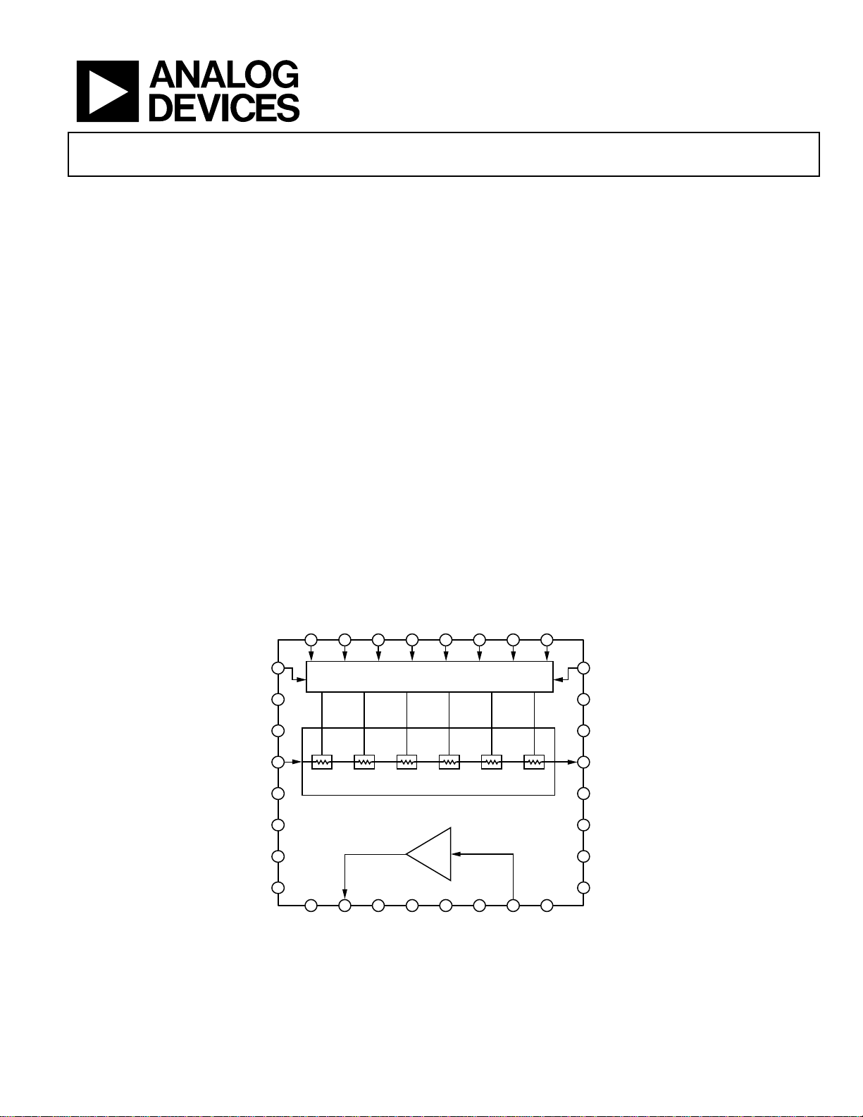
FUNCTIONAL BLOCK DIAGRAM
RF/IF Digitally Controlled VGA
ADL5240
GENERAL DESCRIPTION
The ADL5240 is a high performance, digitally controlled variable
gain amplifier (VGA) operating from 100 MHz to 4000 MHz.
The VGA integrates a high performance, 20 dB gain, internally
matched amplifier (AMP) with a 6-bit digital step attenuator
(DSA) that has a gain control range of 31.5 dB in 0.5 dB steps
with ±0.25 dB step accuracy. The attenuation of the DSA can be
controlled using a serial or parallel interface.
Both the gain block and DSA are internally matched to 50 at
their inputs and outputs and are separately biased. The separate
bias allows all or part of the ADL5240 to be used, which facilitates
easy reuse throughout a design. The pinout of the ADL5240 also
enables either the gain block or DSA to be first, giving the VGA
maximum flexibility in a signal chain.
The ADL5240 consumes just 93 mA and operates from a single
supply ranging from 4.75 V to 5.25 V. The VGA is packaged in a
thermally efficient, 5 mm × 5 mm, 32-lead LFCSP and is fully
specified for operation from −40°C to +85°C. A fully populated
evaluation board is available.
SEL31D0/CLK30D1/DATA29D2/LE28D327D426D525D6
32
1
VDD
2
NC
3
NC
4
DSAIN
NC
NC
NC
NC
Rev. 0
Information furnished by Analog Devices is believed to be accurate and reliable. However, no
responsibility is assumed by Analog Devices for its use, nor for any infringements of patents or other
rights of third parties that may result from its use. Specifications subject to change without notice. No
license is granted by implication or otherwise under any patent or patent rights of Analog Devices.
Trademarks and registered trademarks are the property of their respective owners.
0.5dB 1dB 2dB 4dB 8dB 16dB
5
6
ADL5240
7
8
9NC10
SERIAL/P ARALLEL INTERFACE
11NC12NC13NC14NC15
AMPOUT/VCC
AMP
Figure 1.
24
VDD
23
NC
22
NC
21
DSAOUT
20
NC
19
NC
18
NC
17
NC
16
NC
AMPIN
09430-001
One Technology Way, P.O. Box 9106, Norwood, MA 02062-9106, U.S.A.
Tel: 781.329.4700 www.analog.com
Fax: 781.461.3113 ©2011 Analog Devices, Inc. All rights reserved.
Page 2

ADL5240
TABLE OF CONTENTS
Features.............................................................................................. 1
Applications....................................................................................... 1
General Description ......................................................................... 1
Functional Block Diagram .............................................................. 1
Revision History ............................................................................... 2
Specifications..................................................................................... 3
Absolute Maximum Ratings............................................................ 8
ESD Caution.................................................................................. 8
Pin Configuration and Function Descriptions............................. 9
REVISION HISTORY
7/11—Revision 0: Initial Version
Typical Performance Characteristics........................................... 10
Applications Information.............................................................. 15
Basic Layout Connections......................................................... 15
SPI Timing................................................................................... 17
Loop Performance...................................................................... 19
Thermal Considerations............................................................ 20
Evaluation Board............................................................................ 21
Outline Dimensions....................................................................... 24
Ordering Guide .......................................................................... 24
Rev. 0 | Page 2 of 24
Page 3

ADL5240
SPECIFICATIONS
VDD = 5 V, VCC = 5 V, TA = 25oC
Table 1.
Parameter Test Conditions/Comments Min Typ Max Unit
OVERALL FUNCTION
Frequency Range 100 4000 MHz
AMPLIFIER FREQUENCY = 150 MHz Using the AMPIN and AMPOUT pins
Gain 17.6 dB
vs. Frequency ±50 MHz ±1.0 dB
vs. Temperature −40°C ≤ TA ≤ +85°C ±0.04 dB
vs. Supply 4.75 V to 5.25 V ±0.04 dB
Input Return Loss S11 −10.4 dB
Output Return Loss S22 −7.7 dB
Output 1 dB Compression Point 18.3 dBm
Output Third-Order Intercept ∆f = 1 MHz, P
Noise Figure 2.8 dB
AMPLIFIER FREQUENCY = 450 MHz Using the AMPIN and AMPOUT pins
Gain 20.3 dB
vs. Frequency ±50 MHz ±0.11 dB
vs. Temperature −40°C ≤ TA ≤ +85°C ±0.36 dB
vs. Supply 4.75 V to 5.25 V ±0.01 dB
Input Return Loss S11 −18.3 dB
Output Return Loss S22 −15.7 dB
Output 1 dB Compression Point 20.2 dBm
Output Third-Order Intercept ∆f = 1 MHz, P
Noise Figure 2.9 dB
AMPLIFIER FREQUENCY = 748 MHz Using the AMPIN and AMPOUT pins
Gain 20.6 dB
vs. Frequency ±50 MHz ±0.01 dB
vs. Temperature −40°C ≤ TA ≤ +85°C ±0.31 dB
vs. Supply 4.75 V to 5.25 V ±0.01 dB
Input Return Loss S11 −25.7 dB
Output Return Loss S22 −23.7 dB
Output 1 dB Compression Point 20.2 dBm
Output Third-Order Intercept ∆f = 1 MHz, P
Noise Figure 2.7 dB
AMPLIFIER FREQUENCY = 943 MHz Using the AMPIN and AMPOUT pins
Gain 19.0 20.5 22.0 dB
vs. Frequency ±18 MHz ±0.01 dB
vs. Temperature −40°C ≤ TA ≤ +85°C ±0.27 dB
vs. Supply 4.75 V to 5.25 V ±0.01 dB
Input Return Loss S11 −30.3 dB
Output Return Loss S22 −24.8 dB
Output 1 dB Compression Point 18.5 20.1 dBm
Output Third-Order Intercept ∆f = 1 MHz, P
Noise Figure 2.7 dB
= 4 dBm/tone 30.0 dBm
OUT
= 4 dBm/tone 39.0 dBm
OUT
= 4 dBm/tone 40.0 dBm
OUT
= 4 dBm/tone 40.0 dBm
OUT
Rev. 0 | Page 3 of 24
Page 4

ADL5240
Parameter Test Conditions/Comments Min Typ Max Unit
AMPLIFIER FREQUENCY = 1960 MHz Using the AMPIN and AMPOUT pins
Gain 19.8 dB
vs. Frequency ±30 MHz ±0.03 dB
vs. Temperature −40°C ≤ TA ≤ +85°C ±0.26 dB
vs. Supply 4.75 V to 5.25 V ±0.03 dB
Input Return Loss S11 −11.9 dB
Output Return Loss S22 −12.6 dB
Output 1 dB Compression Point 19.8 dBm
Output Third-Order Intercept ∆f = 1 MHz, P
Noise Figure 2.9 dB
AMPLIFIER FREQUENCY = 2140 MHz Using the AMPIN and AMPOUT pins
Gain 18.0 19.7 22.0 dB
vs. Frequency ±30 MHz ±0.02 dB
vs. Temperature −40°C ≤ TA ≤ +85°C ±0.25 dB
vs. Supply 4.75 V to 5.25 V ±0.04 dB
Input Return Loss S11 −11.0 dB
Output Return Loss S22 −12.0 dB
Output 1 dB Compression Point 17.5 19.5 dBm
Output Third-Order Intercept ∆f = 1 MHz, P
Noise Figure 2.9 dB
AMPLIFIER FREQUENCY = 2630 MHz Using the AMPIN and AMPOUT pins
Gain 18.0 19.6 22.0 dB
vs. Frequency ±60 MHz ±0.01 dB
vs. Temperature −40°C ≤ TA ≤ +85°C ±0.22 dB
vs. Supply 4.75 V to 5.25 V ±0.04 dB
Input Return Loss S11 −11.0 dB
Output Return Loss S22 −13.3 dB
Output 1 dB Compression Point 18.0 19.9 dBm
Output Third-Order Intercept ∆f = 1 MHz, P
Noise Figure 2.9 dB
AMPLIFIER FREQUENCY = 3600 MHz Using the AMPIN and AMPOUT pins
Gain 19.6 dB
vs. Frequency ±100 MHz ±0.03 dB
vs. Temperature −40°C ≤ TA ≤ +85°C ±0.05 dB
vs. Supply 4.75 V to 5.25 V ±0.10 dB
Input Return Loss S11 −15.1 dB
Output Return Loss S22 −12.2 dB
Output 1 dB Compression Point 18.8 dBm
Output Third-Order Intercept ∆f = 1 MHz, P
Noise Figure 3.1 dB
DSA FREQUENCY = 150 MHz Using the DSAIN and DSAOUT pins
Insertion Loss Minimum attenuation −1.5 dB
vs. Frequency ±50 MHz ±0.12 dB
vs. Temperature −40°C ≤ TA ≤ +85°C ±0.09 dB
Attenuation Range 28.8 dB
Attenuation Step Error All attenuation states ±0.18 dB
Attenuation Absolute Error All attenuation states ±1.35 dB
Input Return Loss Minimum attenuation −13.3 dB
Output Return Loss Minimum attenuation −13.4 dB
Input Third-Order Intercept ∆f = 1 MHz, P
= 4 dBm/tone 40.0 dBm
OUT
= 4 dBm/tone 41.0 dBm
OUT
= 4 dBm/tone 41.0 dBm
OUT
= 4 dBm/tone 37.0 dBm
OUT
= 4 dBm/tone, minimum attenuation 45.5 dBm
OUT
Rev. 0 | Page 4 of 24
Page 5

ADL5240
Parameter Test Conditions/Comments Min Typ Max Unit
DSA FREQUENCY = 450 MHz Using the DSAIN and DSAOUT pins
Insertion Loss Minimum attenuation −1.5 dB
vs. Frequency ±50 MHz ±0.02 dB
vs. Temperature −40°C ≤ TA ≤ +85°C ±0.10 dB
Attenuation Range 30.7 dB
Attenuation Step Error All attenuation states ±0.14 dB
Attenuation Absolute Error All attenuation states ±0.42 dB
Input Return Loss Minimum attenuation −17.6 dB
Output Return Loss Minimum attenuation −17.6 dB
Input Third-Order Intercept ∆f = 1 MHz, P
DSA FREQUENCY = 748 MHz Using the DSAIN and DSAOUT pins
Insertion Loss Minimum attenuation −1.6 dB
vs. Frequency ±50 MHz ±0.02 dB
vs. Temperature −40°C ≤ TA ≤ +85°C
Attenuation Range 30.9 dB
Attenuation Step Error All attenuation states ±0.15 dB
Attenuation Absolute Error All attenuation states ±0.32 dB
Input Return Loss Minimum attenuation −17.4 dB
Output Return Loss Minimum attenuation −17.4 dB
Input Third-Order Intercept ∆f = 1 MHz, P
DSA FREQUENCY = 943 MHz Using the DSAIN and DSAOUT pins
Insertion Loss Minimum attenuation −1.6 dB
vs. Frequency ±18 MHz ±0.01 dB
vs. Temperature −40°C ≤ TA ≤ +85°C ±0.12 dB
Attenuation Range 30.9 dB
Attenuation Step Error All attenuation states ±0.13 dB
Attenuation Absolute Error All attenuation states ±0.30 dB
Input Return Loss Minimum attenuation −16.6 dB
Output Return Loss Minimum attenuation −16.5 dB
Input 1 dB Compression Point Minimum attenuation 30.5 dBm
Input Third-Order Intercept ∆f = 1 MHz, P
DSA FREQUENCY = 1960 MHz Using the DSAIN and DSAOUT pins
Insertion Loss Minimum attenuation −2.4 dB
vs. Frequency ±30 MHz ±0.02 dB
vs. Temperature −40°C ≤ TA ≤ +85°C ±0.16 dB
Attenuation Range 31.0 dB
Attenuation Step Error All attenuation states ±0.15 dB
Attenuation Absolute Error All attenuation states ±0.29 dB
Input Return Loss Minimum attenuation −12.0 dB
Output Return Loss Minimum attenuation −11.5 dB
Input 1 dB Compression Point Minimum attenuation 31.5 dBm
Input Third-Order Intercept ∆f = 1 MHz, P
DSA FREQUENCY = 2140 MHz Using the DSAIN and DSAOUT pins
Insertion Loss Minimum attenuation −2.5 dB
vs. Frequency ±30 MHz ±0.02 dB
vs. Temperature −40°C ≤ TA ≤ +85°C
Attenuation Range 31.0 dB
Attenuation Step Error All attenuation states ±0.12 dB
Attenuation Absolute Error All attenuation states ±0.26 dB
Input Return Loss Minimum attenuation −11.9 dB
Output Return Loss Minimum attenuation −11.2 dB
Input 1 dB Compression Point Minimum attenuation 31.5 dBm
Input Third-Order Intercept ∆f = 1 MHz, P
= 4 dBm/tone, minimum attenuation 41.0 dBm
OUT
±0.11
= 4 dBm/tone, minimum attenuation 40 dBm
OUT
= 4 dBm/tone, minimum attenuation 48.5 dBm
OUT
= 4 dBm/tone, minimum attenuation 45.0 dBm
OUT
±0.17
= 4 dBm/tone, minimum attenuation 44.5 dBm
OUT
Rev. 0 | Page 5 of 24
dB
dB
Page 6

ADL5240
Parameter Test Conditions/Comments Min Typ Max Unit
DSA FREQUENCY = 2630 MHz Using the DSAIN and DSAOUT pins
Insertion Loss Minimum attenuation −2.6 dB
vs. Frequency ±60 MHz ±0.04 dB
vs. Temperature −40°C ≤ TA ≤ +85°C ±0.19 dB
Attenuation Range 31.2 dB
Attenuation Step Error All attenuation states ±0.16 dB
Attenuation Absolute Error All attenuation states ±0.19 dB
Input Return Loss Minimum attenuation −13.1 dB
Output Return Loss Minimum attenuation −12.0 dB
Input 1 dB Compression Point Minimum attenuation 31.5 dBm
Input Third-Order Intercept ∆f = 1 MHz, P
DSA FREQUENCY = 3600 MHz Using the DSAIN and DSAOUT pins
Insertion Loss Minimum attenuation −2.8 dB
vs. Frequency ±100 MHz ±0.03 dB
vs. Temperature −40°C ≤ TA ≤ +85°C ±0.21 dB
Attenuation Range 32.1 dB
Attenuation Step Error All attenuation states ±0.37 dB
Attenuation Absolute Error All attenuation states ±0.31 dB
Input Return Loss Minimum attenuation −20.2 dB
Output Return Loss Minimum attenuation −18.2 dB
Input 1 dB Compression Point Minimum attenuation 31.0 dBm
Input Third-Order Intercept ∆f = 1 MHz, P
DIGITAL STEP ATTENUATOR GAIN SETTLING
Minimum Attenuation to Maximum Attenuation 36 ns
Maximum Attenuation to Minimum Attenuation 36 ns
AMP-DSA LOOP FREQUENCY = 943 MHz
Using the AMPIN and DSAOUT pins, DSA at
minimum attenuation
Gain 18.9 dB
vs. Frequency ±18 MHz ±0.01 dB
Gain Range Between maximum and minimum attenuation states 30.8 dB
Input Return Loss S11 −20.5 dB
Output Return Loss S22 −19.7 dB
Output 1 dB Compression Point 18.6 dBm
Output Third-Order Intercept ∆f = 1 MHz, P
Noise Figure 2.7 dB
AMP-DSA LOOP FREQUENCY = 2140 MHz
Using the AMPIN and DSAOUT pins, DSA at
minimum attenuation
Gain 18.2 dB
vs. Frequency ±30 MHz ±0.01 dB
Gain Range Between maximum and minimum attenuation states 31.3 dB
Input Return Loss S11 −14.9 dB
Output Return Loss S22 −16.4 dB
Output 1 dB Compression Point 17.9 dBm
Output Third-Order Intercept ∆f = 1 MHz, P
Noise Figure 3.0 dB
= 4 dBm/tone, minimum attenuation 43.0 dBm
OUT
= 4 dBm/tone, minimum attenuation 43.0 dBm
OUT
= 1 dBm/tone 36.0 dBm
OUT
= 1 dBm/tone 37.5 dBm
OUT
Rev. 0 | Page 6 of 24
Page 7

ADL5240
Parameter Test Conditions/Comments Min Typ Max Unit
AMP-DSA LOOP FREQUENCY = 2630 MHz
Using the AMPIN and DSAOUT pins, DSA at
minimum attenuation
Gain 17.7 dB
vs. Frequency ±60 MHz ±0.11 dB
Gain Range 31.5 dB
Input Return Loss S11 −15.2 dB
Output Return Loss S22 −9.6 dB
Output 1 dB Compression Point 16.9 dBm
Output Third-Order Intercept ∆f = 1 MHz, P
= 1 dBm/tone 33.7 dBm
OUT
Noise Figure 3.0 dB
DSA-AMP LOOP FREQUENCY = 943 MHz
Using the DSAIN and AMPOUT pins, DSA at
minimum attenuation
Gain 18.9 dB
vs. Frequency ±18 MHz ±0.01 dB
Gain Range Between maximum and minimum attenuation states 30.8 dB
Input Return Loss S11 −17.2 dB
Output Return Loss S22 −23.7 dB
Output 1 dB Compression Point 20.2 dBm
Output Third-Order Intercept ∆f = 1 MHz, P
= 4 dBm/tone 40.0 dBm
OUT
Noise Figure 4.4 dB
DSA-AMP LOOP Frequency = 2140 MHz
Using the DSAIN and AMPOUT pins, DSA at
minimum attenuation
Gain 18.0 dB
vs. Frequency ±30 MHz ±0.01 dB
Gain Range Between maximum and minimum attenuation states 31.1 dB
Input Return Loss S11 −13.7 dB
Output Return Loss S22 −10.0 dB
Output 1 dB Compression Point 19.7 dBm
Output Third-Order Intercept ∆f = 1 MHz, P
= 4 dBm/tone 37.5 dBm
OUT
Noise Figure 4.9 dB
DSA-AMP LOOP Frequency = 2630 MHz
Using the DSAIN and AMPOUT pins, DSA at
minimum attenuation
Gain 18.2 dB
vs. Frequency ±60 MHz ±0.01 dB
Gain Range Between maximum and minimum attenuation states 31.7 dB
Input Return Loss S11 −15.7 dB
Output Return Loss S22 −16.9 dB
Output 1 dB Compression Point 19.8 dBm
Output Third-Order Intercept ∆f = 1 MHz, P
= 4 dBm/tone 40.8 dBm
OUT
Noise Figure 5.2 dB
POWER SUPPLIES Using the VDD and VCC pins
Voltage 4.75 5.0 5.25 V
Supply Current
Amplifier 93 120 mA
Digital Step Attenuator 0.5 mA
Rev. 0 | Page 7 of 24
Page 8
ADL5240
ABSOLUTE MAXIMUM RATINGS
Table 2.
Parameter Rating
Supply Voltage (VDD, VCC) 6.5 V
Input Power
AMPIN 16 dBm
DSAIN 30 dBm
Internal Power Dissipation 0.5 W
θJA (Exposed Pad Soldered Down) 36.8°C/W
θJC (Exposed Pad is the Contact) 6.9°C/W
Maximum Junction Temperature 150°C
Lead Temperature (Soldering, 60 sec) 240°C
Operating Temperature Range −40°C to +85°C
Storage Temperature Range −65°C to +150°C
Stresses above those listed under Absolute Maximum Ratings
may cause permanent damage to the device. This is a stress
rating only; functional operation of the device at these or any
other conditions above those indicated in the operational
section of this specification is not implied. Exposure to absolute
ESD CAUTION
maximum rating conditions for extended periods may affect
device reliability.
Rev. 0 | Page 8 of 24
Page 9

ADL5240
2
PIN CONFIGURATION AND FUNCTION DESCRIPTIONS
D4
D3
D6
D5
D2/LE
D1/DATA
SEL
D0/CLK
26
25
27
28
29
30
31
32
1VDD
PIN 1
2NC
INDICATOR
3NC
ADL5240
4DSAIN
5NC
TOP VIEW
(Not to S cale)
6NC
7NC
8NC
9
11
13
12
10
NC
NC
NC
NC
NOTES
1. NC = NO CONNECT . DO NOT CONNECT TO THIS PIN.
. THE EXPOSED PAD MUST BE CONNECTED TO GROUND.
AMPOUT/VCC
24 VDD
23 NC
22 NC
21 DSAOUT
20 NC
19 NC
18 NC
17 NC
15
16
14
NC
NC
AMPIN
09430-002
Figure 2. Pin Configuration
Table 3. Pin Function Descriptions
Pin No. Mnemonic Description
1, 24 VDD Supply Voltage for DSA. Connect this pin to a 5 V supply.
2, 3, 5, 6, 7, 8, 9, 11, 12,
NC No Connect. Do not connect to this pin.
13, 14, 16, 17, 18, 19, 20,
22, 23
4 DSAIN RF Input to DSA.
10 AMPOUT/VCC
RF Output from Amplifier/Supply Voltage for Amplifier. A bias to the amplifier is provided
through a choke inductor connected to this pin.
15 AMPIN RF Input to Amplifier.
21 DSAOUT RF Output from DSA.
25 D6 Data Bit in Parallel Mode (LSB). Connect this pin to the supply in serial mode.
26 D5 Data Bit in Parallel Mode. Connect this pin to ground in serial mode.
27 D4 Data Bit in Parallel Mode. Connect this pin to ground in serial mode.
28 D3 Data Bit in Parallel Mode. Connect this pin to ground in serial mode.
29 D2/LE Data Bit in Parallel Mode/Latch Enable in Serial Mode.
30 D1/DATA Data Bit in Parallel Mode (MSB)/Data in Serial Mode.
31 D0/CLK Connect this pin to ground in parallel mode. This pin functions as a clock in serial mode.
32 SEL
Select Pin. Connect this pin to the supply to select parallel mode operation; connect this
pin to ground to select serial mode operation.
EPAD Exposed Pad. The exposed pad must be connected to ground.
Rev. 0 | Page 9 of 24
Page 10

ADL5240
TYPICAL PERFORMANCE CHARACTERISTICS
45
40
35
30
25
20
15
10
5
NOISE FIGURE, GAIN, P1dB, OIP3 (dB, dBm)
0
0 0.4 0.8 1.2 1.6 2.0 2.4 2.8 3.2 3.6
FREQUENCY (GHz)
Figure 3. AMP: Gain, P1dB, OIP3 at P
Frequency
OIP3
P1dB
GAIN
NF
= 4 dBm/Tone and Noise Figure vs.
OUT
30
28
26
24
22
P1dB (dBm)
20
18
16
09430-003
0 0.4 0.8 1.2 1.6 2.0 2.4 2.8 3.2 3.6
Figure 6. AMP: OIP3 at P
+85°C
+25°C
–40°C
FREQUENCY ( GHz)
= 4 dBm/Tone and P1dB vs. Frequency and
OUT
Temperature
45
40
35
30
25
OIP3 (dBm)
20
15
10
09430-006
21.0
20.5
20.0
19.5
19.0
GAIN (dB)
18.5
18.0
17.5
0 0.4 0.8 1.2 1.6 2.0 2.4 2.8 3.2 3.6
+25°C
FREQUENCY (GHz)
–40°C
+85°C
09430-004
Figure 4. AMP: Gain vs. Frequency and Temperature
0
–5
–10
–15
–20
–25
S-PARAMETERS (d B)
–30
–35
–40
0.1 0.5 0.9 1.3 1.7 2.1 2.5 2.9 3.3 3.7 4.1
S11
FREQUENCY (GHz)
S12
S22
09430-005
Figure 5. AMP: Input Return Loss (S11), Output Return Loss (S22), and Reverse
Isolation (S12) vs. Frequency
46
44
42
748MHz
40
38
36
34
32
OIP3 (dBm)
30
28
26
24
22
–5 1715131197531–1–3
1960MHz
450MHz
2630MHz
Figure 7. AMP: OIP3 vs. P
4.5
4.0
3.5
3.0
2.5
NOISE FIGURE (dB)
2.0
1.5
043.63.22.82.42.01.61.20.80.4
2140MHz
943MHz
150MHz
P
PER TONE (d Bm)
OUT
+85°C
+25°C
–40°C
FREQUENCY (GHz)
3600MHz
and Frequency
OUT
Figure 8. AMP: Noise Figure vs. Frequency and Temperature
09430-007
.0
09430-008
Rev. 0 | Page 10 of 24
Page 11

ADL5240
–
0
–5
–10
–15
–20
–25
ATTENUATIO N ( dB)
–30
–35
–40
0.1 4.13.73.32.92.52.11.71.30.90.5
31.5dB
FREQUENCY (GHz)
Figure 9. DSA: Attenuation vs. Frequency
ATTENUATIO N ( dB)
1
–6
–11
–16
–21
–26
–31
–36
0.1 4.13.73.32.92.52.11.71.30.90.5
4dB
8dB
16dB
31.5dB
FREQUENCY (GHz)
0dB
Figure 10. DSA: Attenuation vs. Frequency and Temperature
0dB
+85°C
+25°C
–40°C
1.0
0.8
0.6
0.4
0.2
0
–0.2
STEP ERROR (dB)
–0.4
–0.6
–0.8
–1.0
0.1 0.5 0.9 1.3 1.7 2.1 2.5 2.9 3.3 3.7 4.1
09430-009
16dB
FREQUENCY (GHz)
30.5dB
31.5dB
31dB
09430-016
Figure 12. DSA: Step Error vs. Frequency, All Attenuation States
1.0
0.8
0.6
0.4
0.2
0
–0.2
–0.4
ABSOLUTE ERRO R (dB)
–0.6
–0.8
–1.0
03282420161284
09430-010
450MHz
2630MHz
ATTENUA TION (dB)
1960MHz
943MHz
748MHz
2140MHz
3600MHz
2
09430-012
Figure 13. DSA: Absolute Error vs. Attenuation
0.5
0.4
0.3
0.2
0.1
–0.1
STEP ERROR (dB)
–0.2
–0.3
–0.4
–0.5
0
032282420161284
450MHz
748MHz
943MHz
1960MHz
2140MHz
2630MHz
3600MHz
ATTENUAT ION (d B)
09430-011
Figure 11. DSA: Step Error vs. Attenuation
0
–5
–10
–15
–20
–25
–30
INPUT RETURN LO SS (d B)
–35
–40
0dB
31.5dB
0.1 4.1
FREQUENCY (GHz)
Figure 14. DSA: Input Return Loss vs. Frequency, All States
3.73.32.92.52.11.71.30.90.5
09430-013
Rev. 0 | Page 11 of 24
Page 12

ADL5240
0
–5
–10
–15
–20
–25
–30
OUTPUT RETURN L O SS (d B)
–35
–40
0dB
31.5dB
0.1 4.1
FREQUENCY (GHz)
Figure 15. DSA: Output Return Loss vs. Frequency, All States
36
35
IIP3
34
33
IP1dB (dBm)
32
3
4
3.73.32.92.52.11.71.30.90.5
09430-014
CH3 2.00V CH4 200mV M10ns 10GS/ s
IT 1.0ps/pt
A CH3 1.24V
09430-018
Figure 18. DSA: Gain Settling Time, 0 dB to 31.5 dB
50
45
40
35
IIP3 (dBm)
30
3
4
31
30
0.9 1.2 1.5 1.8 2.1 2.4 2.7 3.0 3.3 3.6
IP1dB
FREQUENCY (GHz)
Figure 16. DSA: Input P1dB and Input IP3 vs. Frequency,
Minimum Attenuation State
200
150
100
50
0
PHASE (Degrees)
–50
–100
–150
0 4 8 12 16 20 24 28 32
1960MHz
2140MHz
2630MHz
943MHz
ATTENUA TION (dB)
Figure 17. DSA: Phase vs. Attenuation
25
20
09430-015
CH3 2.00V CH4 200mV M10ns 10GS/ s
IT 1.0ps/pt
A CH3 1.24V
09430-019
Figure 19. DSA: Gain Settling Time, 31.5 dB to 0 dB
22
20
18
16
14
12
10
8
6
GAIN AND NOISE FIGURE (dB)
4
2
0
0.1 4.13.73.32.92.52.11.71.30.90.5
09430-017
GAIN
NOISE FIGURE
FREQUENCY (GHz)
09430-020
Figure 20. AMP-DSA Loop: Gain and Noise Figure vs. Frequency,
Minimum Attenuation State
Rev. 0 | Page 12 of 24
Page 13

ADL5240
0
S-PARAMETERS ( dB)
–5
–10
–15
–20
–25
–30
–35
–40
S11
S12
0.1 4.13.73.32.92.52.11.71.30.90.5
FREQUENCY (GHz)
S22
Figure 21. AMP-DSA Loop: Input Return Loss (S11), Output Return Loss (S22),
and Reverse Isolation (S12) vs. Frequency, Minimum Attenuation State
40
38
36
34
32
30
OIP3 (dBm)
28
26
24
22
20
–6 1612 141086420–2–4
2140MHz
Figure 22. AMP-DSA Loop: OIP3 vs. P
P
OUT
2630MHz
(dBm)
943MHz
and Frequency,
OUT
Minimum Attenuation State
22
20
18
16
14
12
10
8
6
GAIN AND NOIS E FIGURE (dB)
4
2
0
0.1 4.13.73.32.92.52.11.71.30.90.5
09430-021
GAIN
NOISE FIGURE
FREQUENCY (GHz)
09430-024
Figure 24. DSA-AMP Loop: Gain and Noise Figure vs. Frequency,
Minimum Attenuation State
0
–5
–10
–15
–20
S-PARAMETERS ( dB)
–25
–30
–35
0.1 0.5 0.9 1.3 1.7 2.1 2.5 2.9 3.3 3.7 4.1
09430-022
S22
S12
FREQUENCY (GHz)
S11
09430-025
Figure 25. DSA-AMP Loop: Input Return Loss (S11), Output Return Loss (S22),
and Reverse Isolation (S12) vs. Frequency, Minimum Attenuation State
20.0
19.5
19.0
18.5
18.0
GAIN (dB)
17.5
17.0
16.5
16.0
–4 2012 14 16 181086420–2
Figure 23. AMP-DSA Loop: Gain vs. P
Minimum Attenuation State
943MHz
2140MHz
2630MHz
P
OUT
(dBm)
and Frequency,
OUT
09430-023
Rev. 0 | Page 13 of 24
44
42
40
943MHz
38
36
34
32
30
28
26
24
–6 1612 141086420–2–4
2140MHz
2630MHz
OIP3 (dBm)
Figure 26. DSA-AMP Loop: OIP3 vs. P
Minimum Attenuation State
P
(dBm)
OUT
and Frequency,
OUT
09430-026
Page 14

ADL5240
20.0
30
19.5
19.0
18.5
18.0
GAIN (dB)
17.5
17.0
16.5
16.0
–4 2012 14 16 181086420–2
Figure 27. DSA-AMP Loop: Gain vs. P
Minimum Attenuation State
110
105
100
95
90
SUPPLY CU RRE NT (mA)
85
943MHz
2140MHz
2630MHz
P
OUT
5.25V
5.00V
4.75V
(dBm)
and Frequency,
OUT
25
20
15
10
PERCENTAGE ( %)
5
0
18.8
18.9
19.0
19.1
19.2
19.3
19.4
19.5
19.6
19.7
19.8
19.9
20.0
20.1
20.2
20.3
20.4
09430-027
P1dB (dBm)
20.5
09430-030
Figure 30. AMP: P1dB Distribution at 2140 MHz
30
25
20
15
10
PERCENTAGE (%)
5
80
–40–30–20–100 102030405060708090
TEMPERAT URE (°C)
Figure 28. AMP: Supply Current vs. Voltage and Temperature
35
30
25
20
15
PERCENTAGE ( %)
10
5
0
18.8
18.9
19.0
19.1
19.2
19.3
19.4
19.5
19.6
19.7
19.8
19.9
20.0
20.1
GAIN (dB)
20.2
Figure 29. AMP: Gain Distribution at 2140 MHz
0
33 34 35 3 6 37 38 39 40 41 42 43 44 45 46 47 48 49 50
09430-028
OIP3 (dBm)
09430-031
Figure 31. AMP: OIP3 Distribution at 2140 MHz
70
60
50
40
30
PERCENTAGE (%)
20
10
0
20.3
20.4
20.5
09430-029
2.0 2.2 2.4 2.6 2.8 3.0 3.2 3.4 3.6 3.8 4.0
NOISE F I GURE (dB)
09430-032
Figure 32. AMP: Noise Figure Distribution at 2140 MHz
Rev. 0 | Page 14 of 24
Page 15

ADL5240
APPLICATIONS INFORMATION
BASIC LAYOUT CONNECTIONS
The basic connections for operating the ADL5240 are shown in Figure 33.
VDD
VDD
SERIAL PARALLEL INTE RFACE
100pF
C6
C8
0.1µF
VCC
32 31 252627282930
D4
D6
D3
D2/LE
NC
NC
NC
D5
DSAOUT
NC
AMPIN
VDD
NC
NC
NC
NC
NC
NC
0.1µF
C1C2
24
23
22
21
20
19
18
17
100pF
C7
AMPIN
SEL
C3
68pF
C4
1.2nF
C5
ADL5240
NC
910 161514131211
D0/CLK
NC D1/DATA
AMPOUT/VCC
1
VDD
2
NC
3
NC
4
DSAIN
5
NC
6
NC
7
NC
8
NC
470nH
L1
0.1µF
DSAIN DSAOUT
AMPOUT
1µF
09430-033
Figure 33. Basic Connections
Rev. 0 | Page 15 of 24
Page 16

ADL5240
Amplifier Bias
The dc bias for the amplifier in ADL5240 is supplied through
Inductor L1 and is connected to the AMPOUT pin. Three
decoupling capacitors (C3, C4, and C5) are used to prevent
RF signals from propagating onto the dc lines. The dc supply
ranges from 4.75 V to 5.25 V and should be connected to the
VCC test point on the evaluation board.
Digital Step Attenuator Bias
The bias for the DSA is provided through the VDD pin. At least
one decoupling capacitor (C8) is recommended on the VDD
trace. The voltage ranges from 4.75 V to 5.25 V and should be
connected to the VDD test point on the evaluation board. The
DSA is shown to work for dc voltages as low as 2.5 V.
Amplifier RF Input Interface
Pin 15 is the RF input for the amplifier of ADL5240. The
amplifier is internally matched to 50 Ω at the input; therefore,
no external components are required. Only a dc blocking
capacitor (C1) is required.
Amplifier RF Output Interface
Pin 10 is the RF output for the amplifier of ADL5240. The
amplifier is internally matched to 50 Ω at the output; therefore,
no external components are required. Only a dc blocking
capacitor (C2) is required. The bias is provided through this pin
via a choke inductor.
DSA RF Input Interface
Pin 4 is the RF input for the DSA of ADL5240. The input
impedance of the DSA is close to 50 Ω over the entire frequency
range; therefore, no external components are required. Only a
dc blocking capacitor (C6) is required.
DSA RF Output Interface
Pin 21 is the RF output for the DSA of ADL5240. The output
impedance of the DSA is close to 50 Ω over the entire frequency
range; therefore, no external components are required. Only a
dc blocking capacitor (C7) is required.
DSA SPI Interface
The DSA of the ADL5240 can operate in either serial or parallel
mode. Pin 32 (SEL) controls the mode of operation. To select serial
mode, connect SEL to ground; to select parallel mode, connect
SEL to VDD. In parallel mode, Pin 25 to Pin 30 (D6 to D1) are
the data bits, with D6 being the LSB. Connect Pin 31 (D0) to
ground during the parallel mode of operation. In serial mode,
Pin 29 is the latch enable (LE), Pin 30 is the data (DATA), and
Pin 31 is the clock (CLK). Pin 26, Pin 27, and Pin 28 are not used
in serial mode and should be connected to ground. Pin 25 (D6)
should be connected to VDD during the serial mode of operation.
To prevent noise from coupling onto the digital signals, an RC filter
can be used on each data line.
Rev. 0 | Page 16 of 24
Page 17

ADL5240
A
SPI TIMING
Tabl e 5 provides details about the timing characteristics for the
SPI signals—namely, the clock (CLK), latch enable (LE), and
data (DATA) signals—and Figure 34 shows the corresponding
SPI timing diagram.
SPI Timing Sequence
Figure 35 is the timing sequence for the SPI function using a 6-bit
operation. The clock can be as fast as 20 MHz. In serial mode,
Register B5 (MSB) is first and Register B0 (LSB) is last.
Table 5. SPI Timing Setup
Parameter Limit Unit Test Conditions/Comments
f
CLK
t
1
t
2
t
3
t
4
t
5
t
6
DATA
10 MHz Data clock frequency
30 ns min Clock high time
30 ns min Clock low time
10 ns min Data to clock setup time
10 ns min Clock to data hold time
10 ns min Clock low to LE setup time
30 ns min LE pulse width
t
1
CLK
t
3
MSB
B5
t
2
t
4
B4 B3 B1
Table 4. Mode Selection Table
Pin 32 (SEL) Functionality
Connect to Ground Serial mode
Connect to Supply Parallel mode
t
5
B2
LSB
B0
t
6
LE
Figure 34. SPI Timing Diagram (Data Is Loaded MSB First), Serial Mode
09430-034
D0/CLK
D1/DAT
D2/LE
D6
MSB
B5
B4 B3 B1
Figure 35. SPI Timing Sequence, Serial Mode
B2
LSB
B0
09430-035
Rev. 0 | Page 17 of 24
Page 18

ADL5240
Table 6. DSA Attenuation Truth Table—Serial Mode
Attenuation State (dB) B5 (MSB) B4 B3 B2 B1 B0 (LSB)
0 (Reference) 1 1 1 1 1 1
0.5 1 1 1 1 1 0
1.0 1 1 1 1 0 1
2.0 1 1 1 0 1 1
4.0 1 1 0 1 1 1
8.0 1 0 1 1 1 1
16.0 0 1 1 1 1 1
31.5 0 0 0 0 0 0
Table 7. DSA Attenuation Truth Table—Parallel Mode
Attenuation State (dB) D1 (MSB) D2 D3 D4 D5 D6 (LSB)
0 (Reference) 1 1 1 1 1 1
0.5 1 1 1 1 1 0
1.0 1 1 1 1 0 1
2.0 1 1 1 0 1 1
4.0 1 1 0 1 1 1
8.0 1 0 1 1 1 1
16.0 0 1 1 1 1 1
31.5 0 0 0 0 0 0
Rev. 0 | Page 18 of 24
Page 19

ADL5240
LOOP PERFORMANCE
The ADL5240 can be configured so that either the DSA precedes
the amplifier (see Figure 36) or the amplifier precedes the DSA
(see Figure 37). The performance of the loop configurations is
presented in Figure 20 to Figure 27. To improve the overall return
loss, a shunt capacitor can be placed between the amplifier and
DSA. This helps to align the phases of the two blocks.
VDD
VDD
SERIAL PARALLEL INTERFACE
RFIN
0.1µF
RFOUT
100pF
C6
C7
0.1µF
VCC
32 31 252627282930
D4
D6
D3
D2/LE
NC
NC
NC
D5
DSAOUT
NC
AMPIN
VDD
NC
NC
NC
NC
NC
NC
24
23
22
21
20
19
18
17
100pF
C1C2
SEL
C3
68pF
C4
1.2nF
C5
ADL5240
NC
910 161514131211
D0/CLK
NC D1/DATA
AMPOUT/VCC
1
VDD
2
NC
3
NC
4
DSAIN
5
NC
6
NC
7
NC
8
NC
470nH
L1
1µF
09430-036
Figure 36. DSA-AMP Loop Configuration
Rev. 0 | Page 19 of 24
Page 20

ADL5240
VDD
VDD
100pF
C7
C2
L1
0.1µF
SERIAL PARALLEL INTE RFACE
32 31 252627282930
SEL
ADL5240
NC
910 161514131211
D0/CLK
AMPOUT/VCC
1
2
3
4
5
6
7
8
VDD
NC
NC
DSAIN
NC
NC
NC
NC
470nH
D4
D3
D5
NC
NC
D6
DSAOUT
NC
AMPIN
VDD
NC
NC
NC
NC
NC
NC
0.1µF
C1
24
23
22
21
20
19
18
17
100pF
C6
RFOUT
RFIN
D2/LE
NC
NC D1/DATA
C3
68pF
C4
VCC
1.2nF
C5
1µF
Figure 37. AMP-DSA Loop Configuration
THERMAL CONSIDERATIONS
The ADL5240 is packaged in a thermally efficient, 5 mm × 5 mm,
32-lead LFCSP. The thermal resistance from junction to air (θ
o
is 36.8
C/W. The thermal resistance for the product was extracted
assuming a standard 4-layer JEDEC board with 25 conductive,
epoxy filled thermal vias. The thermal resistance from junction
to case (θ
lead frame package.
The ADL5240 consumes approximately 93 mA with a 5 V supply
voltage. Even though the part dissipates less than 0.5 W, for the
best thermal performance, it is recommended to add as many
thermal vias as possible under the exposed pad of the LFCSP.
The thermal resistance values given in this section assume a
minimum of 25 thermal vias arranged in a 5 × 5 array with a
diameter of 13 mils and a pitch of 25 mils. Figure 38 shows a
close-up of the thermal via distribution under the exposed pad.
) is 6.9oC/W, where case is the exposed pad of the
JC
09430-037
)
JA
09430-038
Figure 38. Exposed Pad with Thermal Via Distribution
Rev. 0 | Page 20 of 24
Page 21

ADL5240
EVALUATION BOARD
The schematic of the ADL5240 evaluation board is shown in
Figure 39, the evaluation board configuration options are detailed
in Tab l e 8 , and the layout of the ADL5240 evaluation board is
shown in Figure 40 and Figure 41. Each RF trace on the evaluation
board has a characteristic impedance of 50 Ω and is fabricated
on Rogers3003 material. In addition, each trace is a coplanar
waveguide (CPWG) with a width of 25 mils, a spacing of 20 mils,
and a dielectric thickness of 10 mils. The input to and output
from the DSA and amplifier should be ac-coupled with capacitors
of appropriate values to ensure the broadband performance.
The bias to the amplifier is provided by connecting a choke to
the AMPOUT pin. Bypassing capacitors are recommended on
all supply lines to minimize the RF coupling. The DSA and the
amplifier can be individually biased or connected to the VDD
plane using Resistors R2 and R1.
The ADL5240 can be operated in two ways: the amplifier can
precede the DSA (AMP-DSA loop configuration) or the DSA
can precede the amplifier (DSA-AMP loop configuration). The
evaluation board can be configured to handle either option. In
normal operation, R12 and R13 are open, and R10 and R11 are
0 Ω and are used to terminate any RF coupling onto the bypass
trace. To configure the ADL5240 in AMP-DSA loop configuration,
R12 should be replaced with a capacitor, R13 should be replaced
with a 0 Ω resistor, and R10 and R11 should be left open. Similarly,
to configure the ADL5240 in the DSA-AMP loop configuration,
R16 should be replaced with a capacitor, R17 should be replaced
with a 0 Ω resistor, and R14 and R15 should be left open.
The digital signal traces incorporate a footprint for an RC filter
to prevent potential noise from coupling onto the signal. In normal
operation, Resistors R3 to R9 are 0 Ω and Capacitors C9 to C15
are open.
Rev. 0 | Page 21 of 24
Page 22

ADL5240
A
R3
R4
DSAIN
MPOUT
VDD
C1
100pF
0.1µF
0
S1
3
1
R2
DNI
C8
AGND
0
0
2
VDD
AGND
PAD
D0
D2D3D5
SEL
1
VDD
2
NC
NC
4
DSAIN
5
NC
ADL5240
6
DNI
R12
R10
R11
R13
DNI DNI
L1
470nH
C7
68pF
NC
7
NC
8
NC
NC
NC D1
NC
C5
1µF
VCC
AMPOUT/VCC
9
11
101214
AGND
R1
DNI
VDD
AGND AGND
C6
1.2nF
AGND
0.1µF
C4
C9
C10 C11 C13 C14 C15
AGND AGND AGND AGND AGND AGND AGND
25262728293303132
D6
D4
24
VDD
23
NC
22
NC
21
DSAOUT
20
NC
19
NC
18
NC
17
NC
AMPINNCNC
NC
15
13
16
C12
DNI
AGNDAGND
R5
0
0
R6
R7
0
C2
100pF
DNI
R16
R14
0
R15
0
R17
C3
0.1µF
R8
0
0
DNIDNIDNIDNIDNIDNI
DSAOUT
AMPIN
CLKDATA LE
1
2
3
4
5
6
AGND
7
8
9
R9
0
AGND
09430-039
Figure 39. ADL5240 Evaluation Board
Table 8. Evaluation Board Configuration Options
Component Function/Notes Default Value
C1, C2 Input/output dc blocking capacitors for DSA. C1, C2 = 100 pF
C3, C4 Input/output dc blocking capacitors for AMP. C3, C4 = 0.1 μF
C5, C6, C7
Power supply decoupling for amplifier. The bias associated with the AMPOUT pin is
the most sensitive to noise because the bias is connected directly to the output. The
smallest capacitor (C7) should be the closest to the AMPOUT pin.
C5 = 1 μF
C6 = 1.2 nF
C7 = 68 pF
C8 Power supply decoupling for the DSA. C8 = 0.1 μF
C9, C10, C11, C12, C13,
C14, C15
L1
Capacitors of the RC filter on the digital signals leading to the SPI chip.
The bias for the amplifier comes through L1 when VCC is connected to a 5 V supply.
C9, C10, C11, C12,
C13, C14, C15 = open
L1 = 470 nH
L1 should be high impedance for the frequency of operation while providing low
resistance for the dc current.
R1, R2 Resistors to connect the supply for the amplifier and the DSA to the same VDD plane. R1, R2 = open
R3, R4, R5, R6, R7, R8, R9 Resistors of the RC filter on the digital signals leading to the SPI chip.
R3, R4, R5, R6, R7, R8,
R9 = 0 Ω
R10, R11, R14, R15 These resistors are used to terminate RF coupling onto the traces and to close the loop.
R10, R11, R14, R15 =
0 Ω
R12, R13, R16, R17
S1
R12 and R16 are replaced with capacitors, and R13 and R17 are replaced with 0 Ω to
close the loop.
Switch to change between the serial mode and parallel mode of operation. Connect
to supply for parallel mode and to ground for serial mode operation.
R12, R13, R16, R17 =
open
S1 connected to
ground
Rev. 0 | Page 22 of 24
Page 23

ADL5240
09430-041
Figure 40. Evaluation Board Layout—Top
09430-040
Figure 41. Evaluation Board Layout—Bottom
Rev. 0 | Page 23 of 24
Page 24

ADL5240
OUTLINE DIMENSIONS
5.00
INDICATOR
1.00
0.85
0.80
SEATING
PLANE
PIN 1
12° MAX
BSC SQ
4.75
BSC SQ
TOP VIEW
0.80 MAX
0.65 TYP
0.30
0.25
0.18
COMPLIANT TO JEDEC STANDARDS MO-220-VHHD-2
0.20 REF
0.60 MAX
0.05 MAX
0.02 NOM
COPLANARITY
0.08
0.50
BSC
0.50
0.40
0.30
Figure 42. 32-Lead Lead Frame Chip Scale Package [LFCSP_VQ]
5 mm × 5 mm Body, Very Thin Quad
(CP-32-3)
Dimensions shown in millimeters
ORDERING GUIDE
Model1 Temperature Range Package Description Package Option
ADL5240ACPZ-R7 −40°C to +85°C 32 Lead LFCSP_VQ, 7" Tape and Reel CP-32-3
ADL5240-EVALZ Evaluation Board
1
Z = RoHS Compliant Part.
25
24
17
16
0.60 MAX
PIN 1
32
INDICATOR
1
EXPOSED
PAD
BOTTO M V IEW
3.50 REF
FOR PROPE R CONNECTION O F
THE EXPOSE D PAD, REF ER T O
THE PIN CONFIGURATION AND
FUNCTION DE SCRIPTIO NS
SECTION OF THIS DATA SHEET.
3.45
3.30 SQ
3.15
8
9
0.25 MIN
05-25-2011-A
©2011 Analog Devices, Inc. All rights reserved. Trademarks and
registered trademarks are the property of their respective owners.
D09430-0-7/11(0)
Rev. 0 | Page 24 of 24
 Loading...