

Page 1
Wide Dynamic Range, High Speed,
A
Data Sheet
FEATURES
Dual independent, digitally controlled VGAs
−11.5 dB to +20 dB gain range
0.5 dB ± 0.1 dB step size
150 Ω differential input and output
7.5 dB noise figure at maximum gain
OIP3 > 50 dBm at 200 MHz
−3 dB upper frequency bandwidth of 700 MHz
Multiple control interface options
Parallel 6-bit control interface (with latch)
Serial peripheral interface (SPI) (with fast attack)
Gain up/down mode
Wide input dynamic range
Low power mode option
Power-down control
Single 5 V supply operation
40-lead, 6 mm × 6 mm LFCSP package
APPLICATIONS
Differential ADC drivers
High IF sampling receivers
High output power IF amplification
Instrumentation
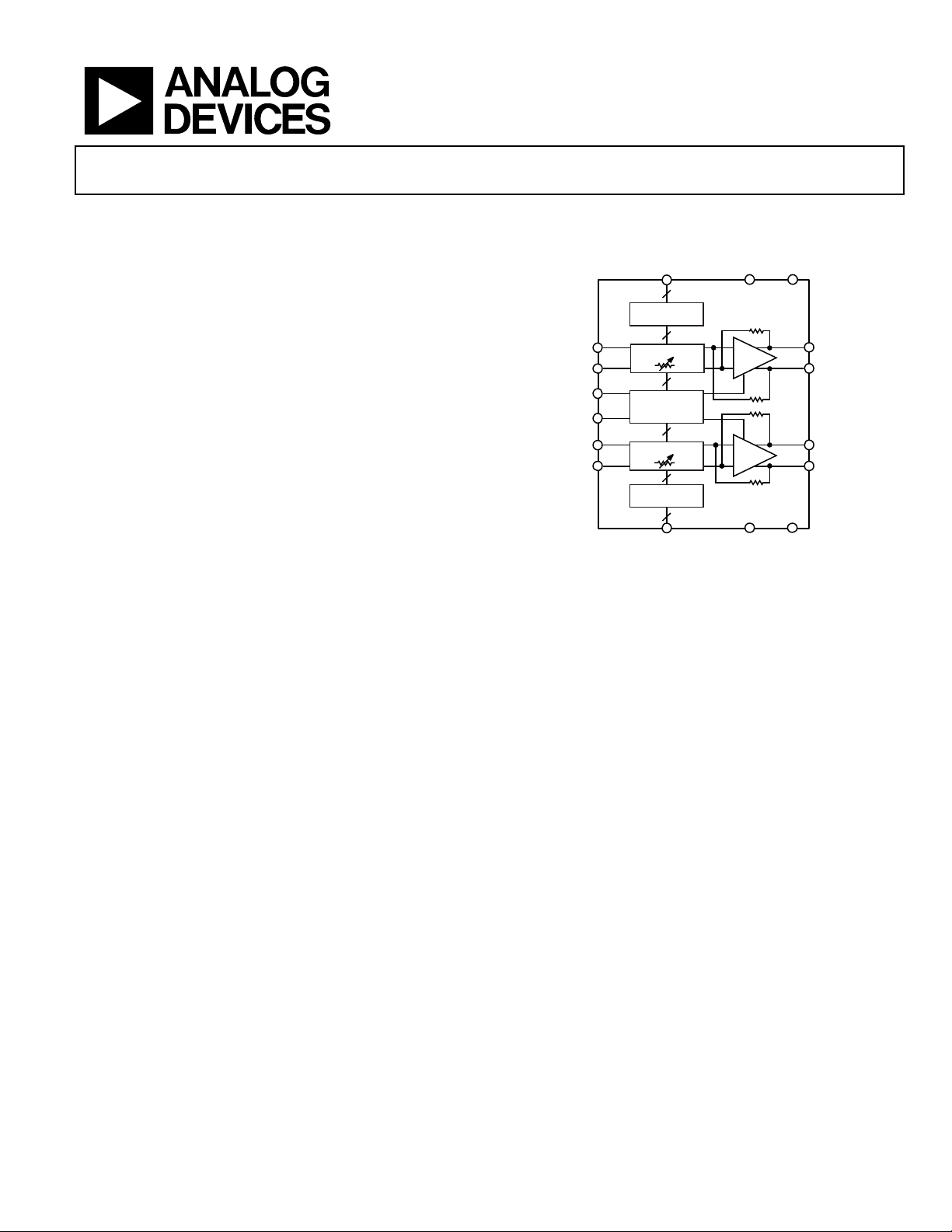
Digitally Controlled VGA
ADL5202
FUNCTIONAL BLOCK DIAGRAM
SIDE
SPI WITH FA,
PARALLEL WITH LATCH,
VINA+
VINA–
MODE0,
MODE1
PM
VINB+
VINB–
UP/DN
LOGIC
0dB TO 31.5d B
150Ω
CONTROL
CIRCUITRY
0dB TO 31.5dB
150Ω
LOGIC
SIDE B
SPI WITH FA,
PARALLEL WITH LATCH,
UP/DN
Figure 1.
PWUPA
+20dB
+20dB
ADL5202
PWUPB
VPOS
150Ω
150Ω
GND
VOUTA+
VOUTA–
VOUTB+
VOUTB–
09387-001
GENERAL DESCRIPTION
The ADL5202 is a digitally controlled, variable gain, wide bandwidth amplifier that provides precise gain control, high output
IP3, and low noise figure. The excellent distortion performance
and high signal bandwidth make the ADL5202 an excellent gain
control device for a variety of receiver applications. The
ADL5202 also incorporates a low power mode option that
lowers the supply current.
For wide input dynamic range applications, the ADL5202
provides a broad 31.5 dB gain range with 0.5 dB resolution. The
gain is adjustable through multiple gain control interface options:
parallel, serial peripheral interface, and up/down.
Incorporating proprietary distortion cancellation techniques,
the ADL5202 achieves a better than 50 dBm output IP3 at
frequencies approaching 200 MHz for most gain settings.
The ADL5202 is powered on by applying the appropriate logic
level to the PWUPx pins. The quiescent current of the ADL5202
is typically 160 mA in low power mode. When configured in high
performance mode for more demanding applications, the quiescent
current is 210 mA. When powered down, the ADL5202 consumes
less than 14 mA and offers excellent input-to-output isolation.
The gain setting is preserved during power-down.
Fabricated on an Analog Devices, Inc., high speed SiGe process,
the ADL5202 provides precise gain adjustment capabilities with
good distortion performance and low phase error. The ADL5202
amplifier comes in a compact, thermally enhanced 40-lead,
6 mm × 6 mm LFCSP package and operates over a temperature
range of −40°C to +85°C.
Rev. 0
Information furnished by Analog Devices is believed to be accurate and reliable. However, no
responsibility is assumed by Anal og Devices for its use, nor for any infringements of patents or ot her
rights of third parties that may result from its use. Specifications subject to change without notice. No
license is granted by implication or otherwise under any patent or patent rights of Analog Devices.
Trademarks and registered trademarks are the property of their respective owners.
One Technology Way, P.O. Box 9106, Norwood, MA 02062-9106, U.S.A.
Tel: 781.329.4700 www.analog.com
Fax: 781.461.3113 ©2011 Analog Devices, Inc. All rights reserved.
Page 2

ADL5202 Data Sheet
TABLE OF CONTENTS
Features.............................................................................................. 1
Applications....................................................................................... 1
Functional Block Diagram ..............................................................1
General Description......................................................................... 1
Revision History ...............................................................................2
Specifications..................................................................................... 3
Absolute Maximum Ratings............................................................ 5
ESD Caution.................................................................................. 5
Pin Configuration and Functional Descriptions.......................... 6
Typical Performance Characteristics............................................. 8
Characterization and Test Circuits............................................... 15
Theory of Operation ......................................................................16
Digital Interface Overview ........................................................ 16
Parallel Digital Interface............................................................ 16
Serial Peripheral Interface (SPI)............................................... 16
Gain Up/Down Interface........................................................... 16
Truth Table.................................................................................. 17
Logic Timing............................................................................... 17
Circuit Description......................................................................... 18
Basic Structure............................................................................ 18
Applications Information.............................................................. 19
Basic Connections...................................................................... 19
ADC Driving............................................................................... 19
Layout Considerations............................................................... 21
Evaluation Board............................................................................ 22
Evaluation Board Control Software......................................... 22
Evaluation Board Schematics and Artwork............................ 23
Evaluation Board Configuration Options............................... 27
Outline Dimensions....................................................................... 29
Ordering Guide .......................................................................... 29
REVISION HISTORY
10/11—Revision 0: Initial Version
Rev. 0 | Page 2 of 32
Page 3

Data Sheet ADL5202
SPECIFICATIONS
VS = 5 V, TA = 25°C, RS = RL = 150 Ω at 100 MHz, high performance mode, 2 V p-p differential output, unless otherwise noted.
Table 1.
Parameter Test Conditions/Comments Min Typ Max Unit
DYNAMIC PERFORMANCE
−3 dB Bandwidth V
Slew Rate
Input Return Loss (S11) 100 MHz
Output Return Loss (S22) 100 MHz
INPUT STAGE
Maximum Input Swing (Differential) Gain code = 111111
Differential Input Resistance
Common-Mode Input Voltage
CMRR Gain code = 000000
GAIN
Maximum Voltage Gain Gain code = 000000 20 dB
Minimum Voltage Gain Gain code = 111111 −11.5 dB
Gain Step Size 0.5 dB
Gain Flatness 30 MHz < fC < 200 MHz 0.285 dB
Gain Temperature Sensitivity Gain code = 000000
Gain Step Response For VIN = 0.2 V, gain code = 111111 to 000000
Gain Conformance Error Over 10 dB gain range
Phase Conformance Error Over 10 dB gain range
OUTPUT STAGE
Output Voltage Swing At P1dB, gain code = 000000
Differential Output Resistance Differential
NOISE/HARMONIC PERFORMANCE
46 MHz Gain code = 000000, high performance mode
Second Harmonic V
Third Harmonic V
Output IP3 V
70 MHz Gain code = 000000, high performance mode
Second Harmonic V
Third Harmonic V
Output IP3 V
140 MHz Gain code = 000000, high performance mode
Noise Figure
Second Harmonic V
Third Harmonic V
Output IP3 V
Output 1 dB Compression Point
300 MHz Gain code = 000000, high performance mode
Second Harmonic V
Third Harmonic V
Output IP3 V
< 2 V p-p (5.2 dBm)
OUT
700
5.5
−17.7
−16.5
MHz
V/ns
dB
dB
VINA+, VINB+ and VINA−, VINB− pins
10.8
150
1.5
40
V p-p
Ω
V
dB
0.012
15 ns
±0.03 dB
1.0 Degrees
dB/°C
VOUTx+ and VOUTx− pins
10
150
V p-p
Ω
= 2 V p-p
OUT
= 2 V p-p
OUT
= 2 V p-p composite
OUT
−92
−105
50
dBc
dBc
dBm
= 2 V p-p
OUT
= 2 V p-p
OUT
= 2 V p-p composite
OUT
−96
−105
50
dBc
dBc
dBm
= 2 V p-p
OUT
= 2 V p-p
OUT
= 2 V p-p composite
OUT
7.5
−86
−105
50
19.5
dB
dBc
dBc
dBm
dBm
= 2 V p-p
OUT
= 2 V p-p
OUT
= 2 V p-p composite
OUT
−77
−91
47
dBc
dBc
dBm
Rev. 0 | Page 3 of 32
Page 4
ADL5202 Data Sheet
Parameter Test Conditions/Comments Min Typ Max Unit
POWER-UP INTERFACE PWUPA, PWUPB pins
Power-Up Threshold Minimum voltage to enable the device 1.4 V
Maximum voltage to enable the device 3.3 V
PWUPx Input Bias Current 1 μA
GAIN CONTROL INTERFACE
VIH Minimum/Maximum voltage for a logic high 1.4 3.3 V
VIL Maximum voltage for a logic low 0.8
Maximum Input Bias Current 1 μA
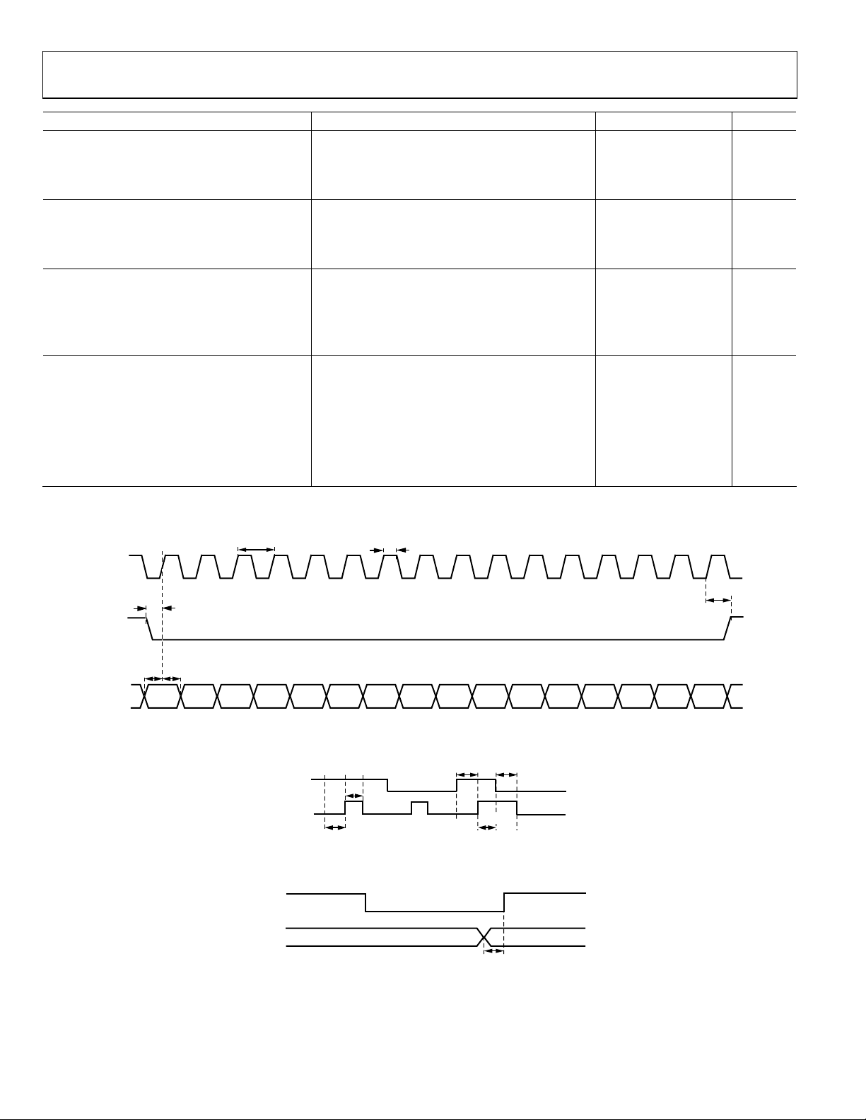
SPI TIMING LATCHA and LATCHB, SCLK, SDIO, data pins
f
1/t
SCLK
tDH Data hold time 5 ns
tDS Data setup time 5 ns
tPW SCLK high pulse width 5 ns
POWER INTERFACE
Supply Voltage 4.5 5.5 V
Quiescent Current, Both Channels High performance mode
T
Low power mode
T
Power-Down Current, Both Channels PWUPx low
Timing Diagrams
t
SCLK
SCLK
20 MHz
SCLK
= 85°C
A
= 85°C
A
210 mA
250 mA
160 mA
180 mA
14 mA
t
PW
t
DH
09387-002
___ ___
CSA, CSB
SDIO
t
DS
tDSt
DH
DNC DNC DNC DNC DNC DNC DNC R/W FA1 FA0 D5 D4 D3 D2 D1 D0
Figure 2. SPI Interface Read/Write Mode Timing Diagram
t
t
DS
DS
UPDN_DAT
UPDN_CLK
t
PW
DNUP
t
DS
RESET
t
DH
09387-103
Figure 3. Up/Down Mode Timing Diagram
LATCHA,
LATCHB
A5 TO A0
B5 TO B0
t
DH
09387-104
Figure 4. Parallel Mode Timing Diagram
Rev. 0 | Page 4 of 32
Page 5
Data Sheet ADL5202
ABSOLUTE MAXIMUM RATINGS
Table 2.
Parameter Rating
Supply Voltage, V
PWUPA, PWUPB, A0 to A5, B0 to B5,
MODE0, MODE1, PM, LATCHA, LATCHB
Input Voltage, V
Internal Power Dissipation 1.6 W
θJA (Exposed Paddle Soldered Down) 34.6°C/W
θJC (At Exposed Paddle) 3.6°C/W
Maximum Junction Temperature 140°C
Operating Temperature Range −40°C to +85°C
Storage Temperature Range −65°C to +150°C
Lead Temperature (Soldering, 60 sec) 240°C
5.5
POS
3.6 V
,VIN− +3.6 V to −1.2 V
IN+
Stresses above those listed under Absolute Maximum Ratings
may cause permanent damage to the device. This is a stress
rating only; functional operation of the device at these or any
other conditions above those indicated in the operational
section of this specification is not implied. Exposure to absolute
maximum rating conditions for extended periods may affect
device reliability.
ESD CAUTION
Rev. 0 | Page 5 of 32
Page 6
ADL5202 Data Sheet
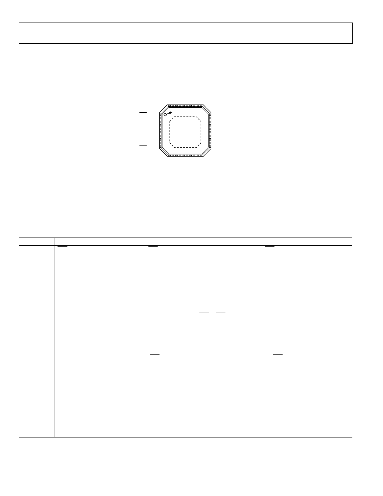
PIN CONFIGURATION AND FUNCTION DESCRIPTIONS
+
A
T
UPA
U
O
GND
PW
VINA+
VINA–
V
VOUTA–
6
31
32
37 LATCHA
3
35
38 UPDN_DAT_A/A0
34
CSA/A3
MODE1
MODE0
PM
GND
SIDO/B5
SCLK/B4
GS1/CSB/B3
39 UPDN_CLK_A/A1
40 FA_A/A2
PIN 1
INDICAT OR
1
2
A4
3
A5
4
5
6
7
8
9
10
ADL5202
TOP VIEW
(Not to Scale)
EXPOSED
PADDLE
33
30
VOUTA–
29
VOUTA+
28
VPOS
27
VPOS
26
VPOS
25
VPOS
VPOS
24
23 VPOS
22
VOUTB+
21
VOUTB–
14
12
13
11
_B/B1
LATCHB
_DAT_B/B0
GS0/FA_B/B2
UPDN_CLK
NOTES
1. NC = NO CONNECT.
2. THE EXPOSED PADDLE (EP) MUST BE CONNECTED TO
A LOW IMPEDANCE GROUND PAD.
UPDN
Figure 5. Pin Configuration
15
VINB–
20
19
16
18
17
UPB
GND
VINB+
PW
VOUTB–
VOUTB+
09387-003
Table 3. Pin Function Descriptions
Pin No. Mnemonic Description
1
/A3 Channel A Select (CSA). When serial mode is enabled, a logic low (0 V ≤ CSA ≤ 0.8 V) selects Channel A.
CSA
Bit 3 for Channel A Parallel Gain Control Interface (A3).
2 A4 Bit 4 for Channel A Parallel Gain Control Interface.
3 A5 Bit 5 (MSB) for Channel A Parallel Gain Control Interface.
4 MODE1 MSB for Mode Control. With the MODE0 pin, selects parallel, SPI, or up/down interface mode.
5 MODE0 LSB for Mode Control. With the MODE1 pin, selects parallel, SPI, or up/down interface mode.
6 PM
Performance Mode. A logic low (0 V ≤ PM ≤ 0.8 V) enables high performance mode. A logic high
(1.4 V ≤ PM ≤ 3.3 V) enables low power mode.
7, 18, 33, EP GND Ground. The exposed paddle (EP) must be connected to a low impedance ground pad.
8 SDIO/B5
Serial Data Input/Output (SDIO). When CSA
or CSB is pulled low, SDIO is used for reading and writing
to the SPI port.
Bit 5 for Channel B Parallel Gain Control Interface (B5).
9 SCLK/B4
Serial Clock Input in SPI Mode (SCLK).
Bit 4 for Channel B Parallel Gain Control Interface (B4).
10
GS1/CSB
/B3 MSB for Gain Step Size Control in Up/Down Mode (GS1).
Channel B Select (CSB
). When serial mode is enabled, a logic low (0 V ≤ CSB≤ 0.8 V ) selects Channel B.
Bit 3 for Channel B Parallel Gain Control Interface (B3).
11 GS0/FA_B/B2
LSB for Gain Step Size Control in Up/Down Mode (GS0).
Fast Attack (FA_B). In serial mode, a logic high (1.4 V ≤ FA_B ≤ 3.3 V) attenuates Channel B according to
the FA setting in the SPI word.
Bit 2 for Channel B Parallel Gain Control Interface (B2).
12 UPDN_CLK_B/B1
Clock Interface for Channel B Up/Down Function (UPDN_CLK_B).
Bit 1 for Channel B Parallel Gain Control Interface (B1).
13 UPDN_DAT_B/B0
Data Pin for Channel B Up/Down Function (UPDN_DAT_B).
Bit 0 for Channel B Parallel Gain Control Interface (B0).
14 LATCHB
Channel B Latch. A logic low (0 V ≤ LATCHB ≤ 0.8 V) allows gain changes on Channel B. A logic high
(1.4 V ≤ LATCHB ≤ 3.3 V) prevents gain changes on Channel B.
Rev. 0 | Page 6 of 32
Page 7

Data Sheet ADL5202
Pin No. Mnemonic Description
15 VINB− Channel B Negative Input.
16 VINB+ Channel B Positive Input.
17 PWUPB Channel B Power-Up. A logic high (1.4 V ≤ PWUPB ≤ 3.3 V) enables Channel B.
19, 21 VOUTB− Channel B Negative Output.
20, 22 VOUTB+ Channel B Positive Output.
23, 24, 25,
26, 27, 28
29, 31 VOUTA+ Channel A Positive Output.
30, 32 VOUTA− Channel A Negative Output.
34 PWUPA Channel A Power-Up. A logic high (1.4 V ≤ PWUPA ≤ 3.3 V) enables Channel A.
35 VINA+ Channel A Positive Input.
36 VINA− Channel A Negative Input.
37 LATCHA
38 UPDN_DAT_A/A0 Data Pin for Channel A Up/Down Function (UPDN_DAT_A).
39 UPDN_CLK_A/A1
40 FA_A/A2
VPOS Positive Power Supply.
Channel A Latch. A logic low (0 V ≤ LATCHA ≤ 0.8 V) allows gain changes on Channel A. A logic high
(1.4 V ≤ LATCHA ≤ 3.3 V) prevents gain changes on Channel A.
Bit 0 for Channel A Parallel Gain Control Interface (A0).
Clock Interface for Channel A Up/Down Function (UPDN_CLK_A).
Bit 1 for Channel A Parallel Gain Control Interface (A1).
Fast Attack (FA_A). In serial mode, a logic high (1.4 V ≤ FA_A ≤ 3.3 V) attenuates Channel A according to
FA setting in the SPI word.
Bit 2 for Channel A Parallel Gain Control Interface (A2).
Rev. 0 | Page 7 of 32
Page 8
ADL5202 Data Sheet
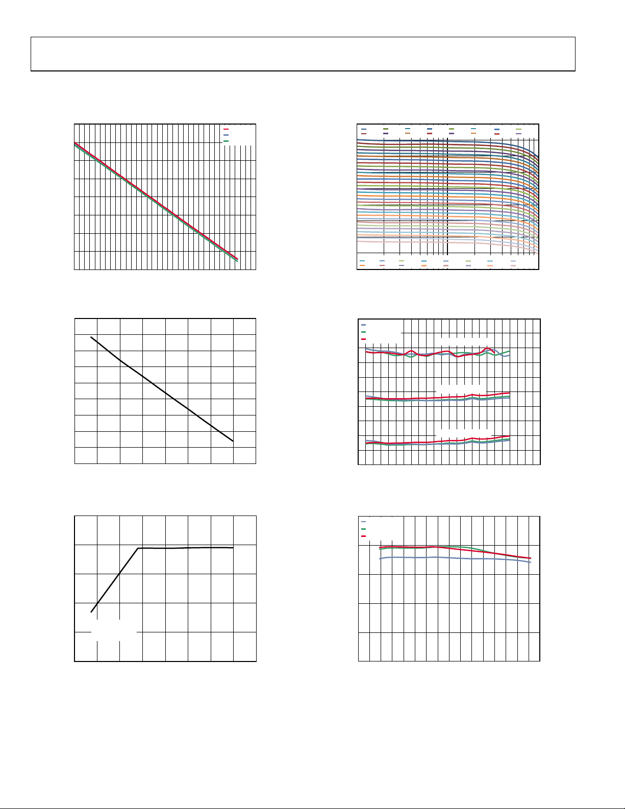
TYPICAL PERFORMANCE CHARACTERISTICS
VS = 5 V, TA = 25°C, RS = RL = 150 Ω at 200 MHz, high performance mode, 2 V p-p differential output, unless otherwise noted.
25
20
15
10
5
GAIN (dB)
0
–5
–10
–15
0 10203040506070
GAIN CODE
46MHz
140MHz
300MHz
Figure 6. Gain vs. Gain Code at 46 MHz, 140 MHz, and 300 MHz
09387-004
25
20dB
19dB
20
15
10
5
0
GAIN (dB)
–5
–10
–15
4dB
3dB
–20
10 100 1000
2dB
1dB
18dB
17dB
0dB
–1dB
16dB
14dB
15dB
13dB
–2dB
–4dB
–3dB
–5dB
FREQUENCY (MHz)
12dB
11dB
–6dB
–7dB
10dB
9dB
–8dB
–9dB
8dB
7dB
Figure 9. Gain vs. Frequency Response (Every 1 dB Step)
6dB
5dB
–10dB
–11dB
09387-007
45
40
35
30
25
20
15
NOISE F IGURE (d B)
10
5
0
–15 –10 –5 0 5 10 15 20 25
PROGRAMMED G AIN (dB)
Figure 7. Noise Figure vs. Programmed Gain at 140 MHz
25
20
15
10
OP1dB (dBm)
50
TA = –40°C
= +25°C
T
A
45
= +85°C
T
A
40
35
30
25
20
NOISE F IGURE (dB)
15
10
5
0
0 100 200 300 400 500 600
09387-010
MIN GAIN (–11.5dB)
MID GAIN (5dB)
MAX GAIN (20dB)
FREQUENC Y (MHz)
09387-013
Figure 10. Noise Figure vs. Frequency at Max, Mid, and Min Gain Outputs
25
TA = –40°C
T
= +25°C
A
= +85°C
T
A
20
15
10
OP1dB (dBm)
INPUT
MAX RATINGS
5
BOUNDARY
0
–15 –10 –5 0 5 10 15 20 25
PROGRAMMED GAIN (dB)
Figure 8. OP1dB vs. Programmed Gain at 140 MHz
09387-005
Rev. 0 | Page 8 of 32
5
0
0 50 100 150 200 250 300 350 400
FREQUENC Y (MHz)
Figure 11. OP1dB vs. Frequency at Maximum Gain, Three Temperatures
09387-008
Page 9
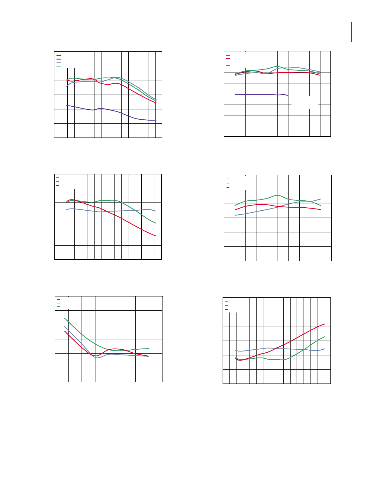
Data Sheet ADL5202
–
–
60
–11.5dB
0dB
10dB
20dB
55
50
45
OIP3 (dBm)
40
35
30
0 50 100 150 200 250 300 350 400
FREQUENCY (MHz)
Figure 12. Output Third-Order Intercept vs. Frequency
at Four Gain Codes
60
TA = –40°C
= +25°C
T
A
= +85°C
T
A
55
50
45
OIP3 (dBm)
40
09387-011
60
–11.5dB
0dB
10dB
55
20dB
50
45
40
OIP3 (dBm)
35
30
25
20
–4–3–2–10123456
P
(dBm)
OUT
INPUT
MAX RATINGS
BOUNDARY
Figure 15. Output Third-Order Intercept vs. Power at Four Gain Codes,
Frequency = 140 MHz at 2 V p-p Composite
60
TA = –40°C
T
= +25°C
A
T
= +85°C
A
55
50
45
OIP3 (dBm)
40
09387-014
35
30
0 50 100 150 200 250 300 350 400
FREQUENCY (MHz)
Figure 13. Output Third-Order Intercept vs. Frequency,
Three Temperatures at 2 V p-p Composite
60
46MHz
140MHz
300MHz
–70
–80
–90
IMD3 (dBc)
–100
–110
–120
–15 –10 –5 0 5 10 15 20 25
PROGRAMMED GAIN (dB)
Figure 14. Two-Tone Output IMD3 vs. Programmed Gain,
at 46 MHz, 140 MHz, 300 MHz
35
30
–4 –3 –2 –1 0 1 2 3 4 5 6
09387-016
P
(dBm)
OUT
09387-019
Figure 16. Output Third-Order Intercept vs. Power, Frequency = 140 MHz,
Three Temperatures
60
TA = –40°C
T
= +25°C
A
T
= +85°C
A
–70
–80
–90
IMD3 (dBc)
–100
–110
–120
09387-018
0 50 100 150 200 250 300 350 400
FREQUENCY (MHz)
09387-021
Figure 17. Two-Tone Output IMD3 vs. Frequency,
Three Temperatures
Rev. 0 | Page 9 of 32
Page 10
ADL5202 Data Sheet
–
–
–
–
–
–
–
–50
–11.5dB
0dB
–60
10dB
20dB
–70
–80
–90
–100
–110
–120
–130
HARMONIC DIS TORTI ON HD2 (dBc)
–140
–150
0 50 100 150 200 250 300 350
FREQUENC Y (MHz)
Figure 18. Harmonic Distortion vs. Frequency at Four Gain Codes
60
TA = –40°C
T
= +25°C
A
–70
T
= +85°C
A
–80
–90
–100
–110
–120
HARMONIC DISTORTION HD2 (dBc)
–130
–30
–40
–50
–60
–70
–80
–90
–100
–110
–120
40
–50
–60
–70
–80
–90
–100
–110
20
HARMONIC DIS TORTI ON HD3 (dBc)
09387-023
60
–11.5dB
0dB
10dB
–70
20dB
–80
–90
–100
–110
–120
HARMONIC DISTORTION HD2 (dBc)
–130
–140
–6 –5 –4 –3 –2 –1 0 1 2 3 4 5 6
P
(dBm)
OUT
40
–50
–60
–70
–80
–90
–100
–110
–120
HARMONIC DISTO RTION HD3 (dBc)
09387-026
Figure 21. Harmonic Distortion vs. Power at Four Gains,
Frequency = 140 MHz
80
TA = –40°C
= +25°C
T
A
= +85°C
T
A
–90
–100
–110
–120
HARMONIC DISTORTION HD3 (dBc)
–130
HARMONIC DISTORTI ON HD2 (dBc)
60
–70
–80
–90
–100
–110
HARMONIC DISTORTI ON HD3 (dBc)
–140
0 50 100 150 200 250 300 350
FREQUENCY (MHz)
–120
Figure 19. Harmonic Distortion vs. Frequency, Three Temperatures
25
20
15
10
OP1dB (dBm)
INPUT
MAX
RATINGS
5
BOUNDARY
0
–15 –10 –5 0 5 10 15 20 25
PROGRAMMED GAIN (dB)
Figure 20. OP1dB vs. Programmed Gain at 140 MHz, Low Power Mode
–140
–6–5–4–3–2–10123456
P
09387-028
OUT
(dBm)
–120
09387-031
Figure 22. Harmonic Distortion vs. Power, Frequency = 140 MHz,
Three Temperatures
25
TA = –40°C
T
= +25°C
A
= +85°C
T
A
20
15
10
OP1dB (dBm)
5
0
0 50 100 150 200 250 300 350 400
09387-006
FREQUENC Y (MHz)
09387-009
Figure 23. OP1dB vs. Frequency at Maximum Gain, Three Temperatures,
Low Power Mode
Rev. 0 | Page 10 of 32
Page 11

Data Sheet ADL5202
–
60
–11.5dB
0dB
10dB
55
20dB
50
60
–11.5dB
0dB
55
10dB
20dB
50
45
45
OIP3 (dBm)
40
35
30
0 50 100 150 200 250 300 350 400
FREQUENCY (MHz)
Figure 24. Output Third-Order Intercept vs. Frequency
at Four Gain Codes, Low Power Mode at 2 V p-p Composite
60
TA = –40°C
T
= +25°C
A
T
= +85°C
A
55
50
45
OIP3 (dBm)
40
35
30
0 50 100 150 200 250 300 350 400
FREQUENCY (MHz)
Figure 25. Output Third-Order Intercept vs. Frequency,
Three Temperatures, Low Power Mode
40
OIP3 (dBm)
35
30
25
20
–4 –3 –2 –1 0 1 2 3 4 5 6
09387-012
P
(dBm)
OUT
INPUT
MAX RATING S
BOUNDRY
09387-015
Figure 27. Output Third-Order Intercept vs. Power at Four Gain Codes,
Frequency = 140 MHz, Low Power Mode
60
TA = –40°C
T
= +25°C
A
55
= +85°C
T
A
50
45
40
OIP3 (dBm)
35
30
25
20
–4 –3 –2 –1 0 1 2 3 4 5 6
P
(dBm)
09387-017
OUT
09387-020
Figure 28. Output Third-Order Intercept vs. Power,
Three Temperatures, Low Power Mode at 2 V p-p Composite
60
46MHz
140MHz
300MHz
–70
–80
–90
IMD3 (dBc)
–100
–110
–120
–15 –10 –5 0 5 10 15 20 25
PROGRAMME D GAIN (dB)
Figure 26. Two-Tone Output IMD3 vs. Programmed Gain
at 46 MHz, 140 MHz, 300 MHz; Low Power Mode
09387-022
Rev. 0 | Page 11 of 32
–60
TA = –40°C
T
= +25°C
A
T
= +85°C
A
–70
–80
–90
IMD3 (dBc)
–100
–110
–120
0 50 100 150 200 250 300 350 400
FREQUENCY (MHz)
Figure 29. Two-Tone Output IMD3 vs. Frequency,
Three Temperatures, Low Power Mode
09387-025
Page 12

ADL5202 Data Sheet
–
–
–
–
–
–
–
–50
–11.5dB
0dB
–60
10dB
20dB
–70
–80
–90
–100
–110
–120
–130
HARMONIC DISTORTION HD2 (dBc)
–140
–150
0 50 100 150 200 250 300 350
FREQUENC Y (MHz)
Figure 30. Harmonic Distortion vs. Frequency at Four Gain Codes,
Low Power Mode
20
–30
–40
–50
–60
–70
–80
–90
–100
–110
–120
60
–11.5dB
0dB
10dB
–70
20dB
–80
–90
–100
–110
–120
HARMONIC DISTORTION HD3 (dBc)
09387-024
HARMONIC DISTORTION HD2 (dBc)
–130
–140
–6 –5 –4 –3 –2 –1 0 1 2 3 4 5 6
P
(dBm)
OUT
Figure 33. Harmonic Distortion vs. Power at Four Gain Codes,
Frequency = 140 MHz, Low Power Mode
40
–50
–60
–70
–80
–90
–100
–110
–120
HARMONIC DISTORTION HD3 (dBc)
09387-027
50
TA = –40°C
= +25°C
T
A
–100
–110
–120
–130
HARMONIC DI STORTION HD2 (d Bc)
–140
–150
–60
–70
–80
–90
= +85°C
T
A
0 50 100 150 200 250 300 350
FREQUENCY (MHz)
Figure 31. Harmonic Distortion vs. Frequency, Three Temperatures,
Low Power Mode
1
4
20
–30
–40
–50
–60
–70
–80
–90
–100
–110
–120
HARMONIC DI STORTION HD3 (d Bc)
70
TA = –40°C
= +25°C
T
A
= +85°C
T
A
–80
–90
–100
–110
–120
HARMONIC DISTORTION HD2 (dBc)
–130
–6 –5 –4 –3
09387-029
–2
–10123456
P
(dBm)
OUT
50
–60
–70
–80
–90
–100
–110
HARMONIC DISTORTION HD3 (dBc)
09387-032
Figure 34. Harmonic Distortion vs. Power, Frequency = 140 MHz, Three
Temperatures, Low Power Mode
CH1 200mV/DIV
VOLTAGE
CH4 1V/DIV
CH1 200mV M 10n s 10GS/ s
ΩCH4 1mV
IT 4ps/pt
Figure 32. Enable Time Domain Response
A CH4 1.12VΩ
09387-036
TIME (10ns/DIV)
09387-033
Figure 35. Disable Time Domain Response
Rev. 0 | Page 12 of 32
Page 13

Data Sheet ADL5202
–
CH2 500mV/DIV
CH3 50mV/DIV
VOLTAGE
TIME (10ns/DI V)
Figure 36. Gain Step Time Domain Response
0
–10
–20
–30
–40
–50
S11 MAGNITUDE (dB)
–60
MAGNITUDE MAX GAIN
–70
MAGNITUDE MIN GAI N
PHASE MAX GAIN
PHASE MIN G AIN
–80
10 100 1000
FREQUENC Y (MHz)
Figure 37. S11 Magnitude and Phase vs. Frequency
200
150
100
50
0
–50
–100
–150
–200
0pf
INPUT
VO LTAG E
200mV/DIV
09387-030
TIME (1ns/DIV)
5.6pf DIF FERENTI AL
09387-034
Figure 39. Large Signal Pulse Response, 0 pF and 5.6 pF, 2 V p-p Composite
0
–10
–20
–30
–40
–50
–60
–70
S11 PHASE (Degrees)
09387-035
S22 MAGNITUDE (dB)
–80
MAGNITUDE MAX GAIN
MAGNITUDE M IN GAIN
–90
PHASE MAX GAIN
PHASE MIN GAIN
–100
10 100 1000
FREQUENCY (MHz)
300
250
200
150
100
50
0
–50
–100
–150
–200
S22 PHASE (Degrees)
09387-038
Figure 40. S22 Magnitude and Phase vs. Frequency
1.0
0.8
0.6
0.4
0.2
0
–0.2
GAIN ERRO R (dB)
–0.4
–0.6
–0.8
–1.0
–15 –10 –5 0 5 10 15 20 25
PROGRAMM ED GAIN ( dB)
Figure 38. Gain Step Error, Frequency = 140 MHz
60
–65
–70
CHANNEL A TO CHANNEL B
CHANNEL A = MAX GAIN
–75
CHANNEL B = ALL G AINS
–80
–85
–90
CHANNEL ISOLAT ION (dB)
–95
–100
0 100 200 300 400 500 600 700 800 900 1000
09387-037
CHANNEL B TO CHANNEL A
CHANNEL B = MAX GAIN
CHANNEL A = ALL G AINS
FREQUENCY (MHz)
09387-043
Figure 41. Channel Isolation vs. Frequency
Rev. 0 | Page 13 of 32
Page 14

ADL5202 Data Sheet
A
L
A
A
A
A
0
0
–10
–20
TION (dB)
–30
–40
REVERSE ISOL
–50
–60
10M 100M 1G
FREQUENC Y (Hz)
Figure 42. Reverse Isolation vs. Frequency
1.0
MIN
MID
MAX
0.8
0.6
Y (ns)
0.4
GROUP DE
0.2
–10
–20
TION (dB)
–30
–40
REVERSE ISOL
–50
–60
10 100 1000
09387-039
FREQUENCY (MHz)
09387-042
Figure 45. Disable-State Reverse Isolation vs. Frequency
60
50
TIO, CMRR (dB)
40
30
20
10
0
10 100 1000
FREQUENCY (MHz)
09387-040
Figure 43. Group Delay vs. Frequency at Max, Mid, and Min Gain Outputs
4.0
3.5
3.0
350MHz
2.5
300MHz
250MHz
TION (Deg rees)
PHASE VARI
200MHz
2.0
150MHz
100MHz
1.5
1.0
0.5
50MHz
0
0 10203040506070
GAIN CODE
09387-041
Figure 44. Phase Variation vs. Gain Code
COMMON- MODE REJECTIO N R
0
10M 100M 1G
FREQUENC Y (Hz)
09387-044
Figure 46. Common-Mode Rejection Ratio vs. Frequency
Rev. 0 | Page 14 of 32
Page 15

Data Sheet ADL5202
V
A
V
CHARACTERIZATION AND TEST CIRCUITS
+5
L1
1µHL21µH
50Ω
C
50Ω
0.1µF
0.1µF
1/2
ADL5202
6
A0 TO A5
Figure 47. Test Circuit for S-Parameters on Dedicated 50 Ω Differential-to-Differential Board
+5
L1
50Ω
AC
TC3-1T
T1
C1
0.1µF
C2
0.1µF
A0 TO A5
1/2
ADL5202
6
1µHL21µH
Figure 48. Test Circuit for Distortion, Gain, and Noise
0.1µF
50Ω TRACES50Ω TRACES
0.1µF
C3
R1
0.1µF
62Ω
PAD LOSS = 11dB
R2
C4
62Ω
0.1µF
R4
25Ω
R3
25Ω
ETC1-1-13
50Ω
AC
50Ω
09387-060
T2
50Ω
09387-062
09387-063
Figure 49. Differential-to-Differential Characterization Board,
Circuit Side Layout
Rev. 0 | Page 15 of 32
Page 16

ADL5202 Data Sheet
THEORY OF OPERATION
DIGITAL INTERFACE OVERVIEW
The ADL5202 VGA has three digital gain control options:
the parallel control interface, serial peripheral interface, and gain
up/down interface. The desired gain control option is selected
via two control pins, MODE0 and MODE1 (see Table 4 for the
truth table for the mode control pins). The gain code is in a 6-bit
binary format. A voltage of between 1.4 V and 3.3 V is required
for a logic high.
Three pins are common to all gain control options: PM, PWUPA,
and PWUPB. PM allows the user to choose operation in nominal
mode or high performance mode. PWUPA and PWUPB are
power-up pins for Channel A and Channel B, respectively.
Physical pins are shared among the three interfaces, resulting in
as many as three different functions per digital pin (see Table 3).
Table 4. Digital Control Interface Selection Truth Table
MODE1 MODE0 Interface
0 0 Parallel control
0 1 Serial peripheral (SPI)
1 0 Up/down
1 1 Up/down
PARALLEL DIGITAL INTERFACE
The parallel digital interface uses six binary bits (Bits[A5:A0] or
Bits[B5:B0]) and a latch pin (LATCHA or LATCHB) per amplifier.
The latch pin controls whether the input data latch is transparent
or latched. In transparent mode, gain changes as input gain control
bits change. In latched mode, gain is determined by the latched
gain setting and does not change with changing input gain
control bits.
SERIAL PERIPHERAL INTERFACE (SPI)
CSA
The SPI uses three pins (SDIO, SCLK, and
SPI data register consists of two bytes: six gain control bits, two
attenuation step size address bits, one read/write bit, and seven
don’t care bits. SDIO is the serial data input and output pin. The
SCLK pin is the serial clock, and
CSA
or
CSB
select pin.
LSB LSBMSB MSB
DATA
D0 D1 D2 D3 D4 D5 FA0 FA1 R/W DNC DNC DNC DNC DNC DNC DNC
FAST ATTACK ATTENUATION
STEP SIZE ADDRESS
GAIN CONTROL
Figure 50. 16-Bit SPI Register
CSA
To write to the SPI register,
CSB
or
must be pulled low and
16 clock pulses must be applied to SCLK. Individual channel
SPI registers can be selected by pulling
pulling the
CSA
and
CSB
pins low simultaneously, the same
CSA
data can be written to both SPI registers.
CSB
or
is the channel
DO NOT CARE
(7 BITS)
READ/WRITE
CSB
or
low. By
). The
09387-046
To read the SPI register value, the R/W bit must be set high,
CSA
CSB
or
must be pulled low, and the part must be clocked.
After the register has been read out during the next 16 clock cycles,
the SPI is automatically put into write mode. Note that there is
only one SDIO pin. Readback from the registers should be performed individually.
Fast Attack
The fast attack feature, accessible via the SPI, allows the gain to be
reduced from its present gain setting by a predetermined step size.
Four different attenuation step sizes are available. The truth table
for fast attack is shown in Tab le 5 .
Table 5. SPI 2-Bit Attenuation Step Size Truth Table
FA1 FA 0 Step Si ze (dB)
0 0 2
0 1 4
1 0
1 1 16
8
SPI fast attack mode is controlled by the FA_A or FA_B pin.
A logic high on the FA_A or FA_B pin results in an attenuation
that is selected by Bits[FA1:FA0] in the SPI register.
GAIN UP/DOWN INTERFACE
The GS1 and GS0 pins control the up/down gain step function.
Gain is increased by a clock pulse on the UPDN_CLK_A pin or
the UPDN_CLK_B pin (rising and falling edges) when the
UPDN_DAT_A or UPDN_DAT_B pin is high. Gain is decreased
by a clock pulse on the UPDN_CLK_A or UPDN_CLK B pin
when the UPDN_DAT_A or UPDN_CLKB pin is low. The truth
table for the gain step function is shown in Table 6. Reset is
detected by a rising edge latching data having one polarity, with
the falling edge latching the opposite polarity. Reset results in
a minimum binary gain code of 111111.
Table 6. Step Size Control Truth Table
GS1 GS0 Step Size (dB)
0 0 0.5
0 1 1
1 0
1 1 4
The step size is selectable using the GS1 and GS0 pins. The gain
is limited by the top and bottom of the control range.
UPDN_DAT
UPDN_CLK
DNUP RESET
Figure 51. Up/Down Timing
2
09387-045
Rev. 0 | Page 16 of 32
Page 17

Data Sheet ADL5202
TRUTH TABLE
Table 7. Gain Code vs. Voltage Gain Lookup Table
6-Bit Binary
Gain Code
000000 20 100000 4
000001 19.5 100001 3.5
000010 19 100010 3
000011 18.5 100011 2.5
000100 18 100100 2
000101 17.5 100101 1.5
000110 17 100110 1
000111 16.5 100111 0.5
001000 16 101000 0
001001 15.5 101001 −0.5
001010 15 101010 −1
001011 14.5 101011 −1.5
001100 14 101100 −2
001101 13.5 101101 −2.5
001110 13 101110 −3
001111 12.5 101111 −3.5
010000 12 110000 −4
010001 11.5 110001 −4.5
010010 11 110010 −5
010011 10.5 110011 −5.5
010100 10 110100 −6
010101 9.5 110101 −6.5
010110 9 110110 −7
010111 8.5 110111 −7.5
011000 8 111000 −8
011001 7.5 111001 −8.5
011010 7 111010 −9
011011 6.5 111011 −9.5
011100 6 111100 −10
011101 5.5 111101 −10.5
011110 5 111110 −11
011111 4.5 111111 −11.5
SCLK
Voltage
Gain (dB)
6-Bit Binary
Gain Code
t
SCLK
Voltage
Gain (dB)
t
PW
LOGIC TIMING
To write to the ADL5202, refer to the timing shown in Figure 2
(reproduced in this section as Figure 52). The write mode uses
a 16-bit serial word on the SDIO pin. The R/W of the word must be
low to write Bits[D0:D5], which are the binary weighted codes for
the attenuation level (0 = minimum attenuation, 63 = maximum
attenuation). The FA0 and FA1 bits control the fast attack step size.
The DNC bits are nonfunctional, do not care bits. Reading the
ADL5202 SPI register requires the following two steps:
1. Set the R/W bit high using a 16-bit word and the timing
described in this section and Figure 52. All other bits are
ignored when the R/W bit is high.
2. The SDIO is used as an output during the next sequence.
The written pattern is serially clocked out on SDIO using
16 clocks and the timing described in this section and
Figure 52. The R/W bit automatically returns low to the
write state following the read sequence.
t
DH
09387-152
___ ___
CSA, CSB
SDIO
t
DS
tDSt
DH
DNC DNC DNC DNC DNC DNC DNC R/W FA1 FA0 D5 D4 D3 D2 D1 D0
Figure 52. SPI Interface Read/Write Mode Timing Diagram
Rev. 0 | Page 17 of 32
Page 18

ADL5202 Data Sheet
CIRCUIT DESCRIPTION
BASIC STRUCTURE
The ADL5202 is a dual, differential, variable gain amplifier,
with each amplifier consisting of a 150 digitally controlled,
passive attenuator that is followed by a highly linear
transconductance amplifier with feedback.
1/2 OF
ADL5202
VIN+
VIN–
ATTENUAT OR
LOGIC REF
DIGITAL INPUTS
PARALLEL, SPI,
FAST ATTACK
UP/DOWN
Figure 53. Simplified Schematic
g
AMP
m
Input System
The dc voltage level at the inputs of each amplifier is set by two
independent internal voltage reference circuits to approximately
1.6 V. The references are not accessible and cannot be adjusted.
Each amplifier can be powered down by pulling the correspond-
ing power-up pin down to ground (logic low). When powered
down, the total current of each amplifier reduces to 7 mA
(typical). The dc level at the inputs remains at approximately
1.6 V, regardless of the state of the PWUPA or PWUPB pin.
Output Amplifier
The gain of the output amplifier is set to 22 dB when driving
a 150 load. The input and output resistance of this amplifier
is set to 150 Ω in matched condition. If the load or the source
resistance is different from 150 Ω, the following equations can
be used to determine the resulting gain and input/output
resistances.
Voltage Gain = A
R
= (2000 + RL)/(1 + 0.09 × RL)
IN
S21 (Gain) = 2 × R
R
= (2000 + RS)/(1 + 0.09 × RS)
OUT
= 0.09 × (2000)//RL
V
/(RIN + RS) × AV
IN
Note that at the maximum attenuation setting, R
the output amplifier, is the output resistance of the attenuator,
which is 150 Ω. However, at minimum attenuation, R
source resistance that is connected to the input of the part.
VOUT+
VOUT–
, as seen by
S
is the
S
09387-047
The dc current to the outputs of each amplifier is supplied through
two external chokes. The inductance of the chokes and the
resistance of the load, in parallel with the output resistance of
the device, add a low frequency pole to the response. The parasitic capacitance of the chokes adds to the output capacitance of the
part. This total capacitance, in parallel with the load and output
resistance, sets the high frequency pole of the device. Generally,
the larger the inductance of the choke, the higher its parasitic
capacitance. Therefore, this trade-off must be considered when
the value and type of the choke are selected. For an operation
frequency of 15 MHz to 700 MHz driving a 150 load, 1 H
chokes with a self resonant frequency (SRF) of 160 MHz or
higher are recommended (such as the 0805LS-102XJBB from
Coilcraft). If higher value chokes are used, a 4 MHz zero, due to
the internal ac-coupled feedback, causes an increase in S21 of up
to 6 dB at frequencies below 4 MHz. The supply current of each
amplifier consists of about 35 mA through the VPOS pin and 50
mA through the two chokes combined. The latter increases with
temperature at approximately 2.5 mA per 10°C. The total choke
current increases to 75 mA for high performance mode. Each
amplifier has two output pins for each polarity, and they are
oriented in an alternating fashion. When designing the board,
care should be taken to minimize the parasitic capacitance due to
the routing that connects the corresponding outputs together.
To minimize the parasitic capacitance, a good practice is to
avoid any ground or power plane under this routing region and
under the chokes.
Gain Control
The gain of each amplifier can be adjusted using the parallel control
interface, the serial peripheral interface, or the gain up/down
interface. In general, the gain step size is 0.5 dB, but larger sizes
can be programmed using the various interfaces, as described in
the Digital Interface Overview section. Each amplifier has a
maximum gain of +20 dB (Code 0) to −11.5 dB (Code 63).
The noise figure of each amplifier is approximately 7.5 dB at
maximum gain setting, and it increases as the gain is reduced.
The increase in noise figure is equal to the reduction in gain.
The linearity of the part measured at the output is first-order
independent of the gain setting. From −4 dB to +20 dB gain,
OIP3 is approximately 50 dBm into 150 load at 200 MHz
(0 dBm per tone). At gain settings below −4 dB, OIP3 drops to
approximately 40 dBm.
Rev. 0 | Page 18 of 32
Page 19

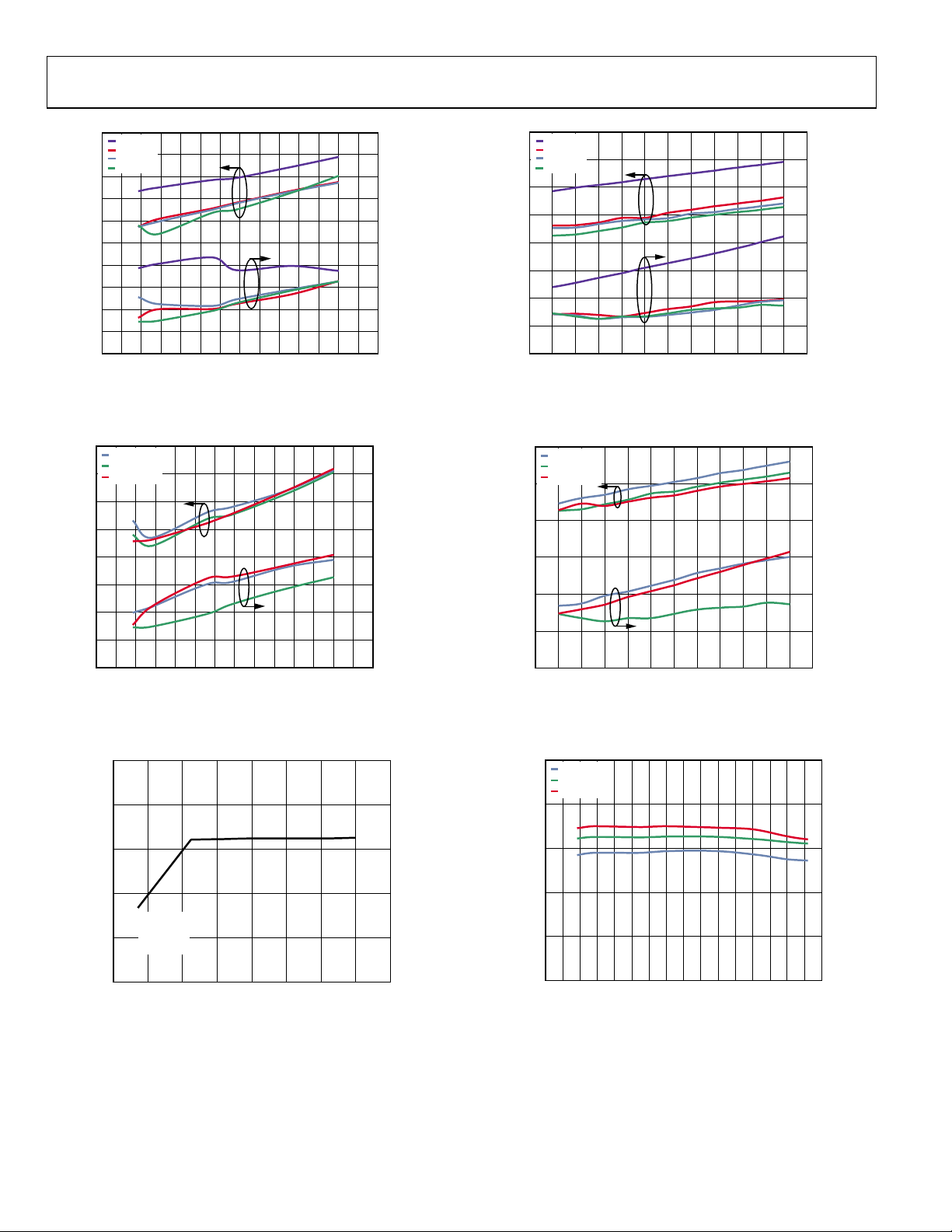
Data Sheet ADL5202
APPLICATIONS INFORMATION
BASIC CONNECTIONS
Figure 54 shows the basic connections for operating the ADL5202.
A voltage between 4.5 V and 5.5 V should be applied to the VPOS
pins. Each supply pin should be decoupled with at least one low
inductance, surface-mount ceramic capacitor of 0.1 F, placed
as close as possible to the device.
The outputs of the ADL5202 must be pulled up to the positive
supply with 1 µH RF chokes. The differential outputs are biased
to the positive supply and require ac coupling capacitors, preferably 0.1 µF. Similarly, the input pins are at bias voltages of
about 1.6 V above ground and should be ac-coupled as well.
The ac coupling capacitors and the RF chokes are the principle
limitations for operation at low frequencies.
The digital pins (mode control pins, associated SPI and parallel
gain control pins, PM, PWUPA, and PWUPB) operate on a voltage
of 3.3 V.
BALANCED
SOURCE
R
R
S
S
AC
2
2
To enable each channel of the ADL5202, the PWUPA or PWUPB
pin must be pulled high (1.4 V≤ PWUPA/PWUPB ≤ 3.3 V).
Taking PWUPA or PWUPB low puts the channels of the ADL5202
in sleep mode, reducing current consumption to approximately
7 mA per channel at ambient.
ADC DRIVING
The ADL5202 is a highly linear, variable gain amplifier that
is optimized for ADC interfacing. The output IMDs and noise
floor remain constant throughout the 31.5 dB gain range.
This is a valuable feature in a variable gain receiver where it is
desirable to maintain a constant instantaneous dynamic range
as the receiver range is modified. The output noise is 18 nV/√Hz,
which is compatible with 14- or 16-bit ADCs. The two-tone
IMDs are usually greater than −100 dB for −1 dBm into 150 Ω
or 2 V p-p output. The 150 Ω output impedance makes the task
of designing a filter for the high input impedance ADCs more
straightforward.
GAIN MODE
INTERFACE
CHANNEL A
GAIN CO NTROL INTERFACE
1
CSA/A3
2
A4
3
A5
4
MODE1
5
MODE0
6
3.3V
CHANNEL B
GAIN CO NTROL INTERFACE
PM
7
GND
8
SIDO/B5
9
SCLK/B4
10
GS1/CSB/
B3
35
36
CHA
VINA–
LAT
ADL5202
EXPOSED
PADDLE
VINB–
LATCHB
15
16
VINA+
VINB+
0.1µF
3.3V
34
17
3.3V
0.1µF0.1µF
31
32
33
+
A
UPA
PW
UPB
PW
18
T
GND
U
O
VOUTA–
V
VOUTA–
VOUTA+
VPOS
VPOS
VPOS
VPOS
VPOS
VPOS
VOUTB+
VOUTB–
VOUTB+
VOUTB–
GND
0
2
19
30
29
28
27
26
25
24
23
22
21
0.1µF
0.1µF
0.1µF
0.1µF
0.1µF
0.1µF
1µH
1µH
1µH
VPOS
1µH
0.1µF
0.1µF
0.1µF
0.1µF
0.1µF
0.1µF
R
L
R
L
BALANCED
LOAD
VPOS
BALANCED
LOAD
VPOS
0.1µF
37
38
39
40
FA_A/A2
UPDN_DAT_A/A0
UPDN_CLK_A/A1
_DAT_B/B0
FA_B/B2
GS0/
UPDN_CLK_B/B1
UPDN
12
13
11
14
R
R
S
S
AC
2
2
BALANCED
SOURCE
09387-048
Figure 54. Basic Connections
Rev. 0 | Page 19 of 32
Page 20

ADL5202 Data Sheet
A
V
5V
0.1µF
1:3
50Ω
C
0.1µF
1/2
ADL5202
DIGIT AL
INTERF ACE
5
1.0µH
1.0µH
5V
Figure 55. Wideband ADC Interfacing Example Featuring One-Half of the ADL5202 and the AD9268
Figure 55 shows one-half of the ADL5202 driving a two-pole,
100 MHz low-pass filter into the AD9268. The AD9268 is
a 16-bit, 125 MSPS analog-to-digital converter with a buffered
wideband input, which presents a 6 k differential input impedance and requires between a 1 V or 2 V input swing to reach
full scale. This example uses the 2 V p-p input. For optimum
performance, the ADL5202 should be driven differentially,
using an impedance transformer or input balun.
0
–1
–2
–3
–4
–5
–6
–7
–8
–9
–10
INSERTION LOSS (dB)
–11
–12
–13
–14
–15
0 20 40 60 80 100 120 140 160 180 200
FREQUENCY (MHz)
09387-050
Figure 56. Measured Frequency Response of Wideband
ADC Interface, as Depicted in Figure 55
Figure 55 uses a 1:3 impedance transformer to provide the 150 Ω
input impedance of the ADL5202 with a matched input. The
outputs of the ADL5202 are biased through the two 1 µH
inductors, and the two 0.1 µf capacitors on the outputs decouple
the 5 V inductor voltage from the input common-mode voltage of
the AD9268. The two 75 Ω resistors provide the 150 Ω load to the
ADL5202 whose gain is load dependent. The 56 nH inductors
and 4 pF capacitor constitute the (100 MHz – 1 dB) low-pass
filter. The two 33 Ω isolation resistors suppress any switching
currents from the ADC input sample-and-hold circuitry. The
circuit depicted in Figure 55 provides variable gain, isolation,
filtering, and source matching for the AD9268. Using this circuit
with the ADL5202 in a gain of 20 dB (maximum gain), an SNR
of 69 dB, and an SFDR performance of >86 dBc is achieved at
100 MHz, as shown in Figure 57.
0.1µF
0.1µF
V
REF
56nH
33Ω
75Ω
V
REF
75Ω
56nH
0
–15
–30
–45
–60
–75
–90
AMPLITUDE (dBFS)
–105
–120
–135
–150
0 6 12 18 24 30 36 42 48 54 60
4pF
33Ω
5
AD9268
+
4
6
FREQUENCY (MHz)
09387-049
SNR = 69dB
SFDR = 86dBc
NOISE F LOO R = –108dB
FUND = –1.035dBFS
SECOND = –89.17dBc
3
2
09387-051
Figure 57. Measured Single-Tone Performance of the
Circuit in Figure 55 for a 100 MHz Input Signal
0
–15
–30
–45
–60
–75
–90
F2 – F1
AMPLITUDE (dBFS)
–105
–120
–135
–150
0 6 12 18 24 30 36 42 48 54 60
Figure 58. Measured Two-Tone Performance of the
Circuit in Figure 55 for a 100 MHz Input Signal
FUNDAMENTAL 1 = –7.127dBFS
FUNDAMENTAL 2 = –7.039dBFS
2F1 – F2 = –91.818dBc
2F2 – F1 = –87.083dBc
NOISE FL OOR = –109.57dB
+
2F1 – F22F2 – F1
FREQUENCY (MHz)
2F1 + F2
F1 + F2
2F2 + F1
09387-052
Rev. 0 | Page 20 of 32
Page 21

Data Sheet ADL5202
A
V
An alternative narrow-band approach is presented in Figure 59.
By designing a narrow band-pass antialiasing filter between the
ADL5202 and the target ADC, the output noise of the ADL5202
outside of the intended Nyquist zone can be attenuated, helping
to preserve the available SNR of the ADC. In general, the SNR
improves by several decibels (dB) when including a reasonable
order antialiasing filter. In this example, a low loss 1:3 input
transformer is used to match the 150 balanced input of the
ADL5202 to a 50 unbalanced source, resulting in minimum
insertion loss at the input.
Figure 59 is optimized for driving some of the Analog Devices
popular unbuffered ADCs, such as the AD9246, AD9640,
and AD6655. Table 8 includes antialiasing filter component
recommendations for popular IF sampling center frequencies.
Inductor L5 works in parallel with the on-chip ADC input
capacitance and a portion of the capacitance presented by C4 to
form a resonant tank circuit. The resonant tank helps to ensure
that the ADC input acts like a real resistance at the target center
frequency.
5
In addition, the L6 inductor shorts the ADC inputs at dc, which
introduces a zero into the transfer function. The ac coupling
capacitors and the bias chokes introduce additional zeros into the
transfer function. The final overall frequency response takes on
a band-pass characteristic, helping to reject noise outside of the
intended Nyquist zone. Tab le 8 provides initial suggestions for
prototyping purposes. Some empirical optimization may be
needed to help compensate for actual PCB parasitics.
LAYOUT CONSIDERATIONS
Each amplifier has two output pins for each polarity, and they
are oriented in an alternating fashion. When designing the board,
care should be taken to minimize the parasitic capacitance due
to the routing that connects the corresponding outputs together.
A good practice is to avoid any ground or power plane under
this routing region and under the chokes to minimize the
parasitic capacitance.
50Ω
C
1:3
5V
1nF
1/2
ADL5202
1nF
DIGITAL
INTERFACE
Figure 59. Narrow-Band IF Sampling Solution for Unbuffered ADC Applications
1µH
1nF
L1 L3 L5
C4
4pF
75Ω
75Ω
CML
L6
C2
4pF
L1 L3 L5
1nF
1µH
5V
AD9246
AD9640
AD6655
09387-053
Table 8. Interface Filter Recommendations for Various IF Sampling Frequencies
Center Frequency 1 dB Bandwidth L1 C2 L3 C4 L5 L6
96 MHz 27 MHz 68 nH 15 pF 220 nH 15 pF 68 nH 150 nH
140 MHz 31 MHz 47 nH 11 pF 150 nH 11 pF 47 nH 82 nH
170 MHz 25 MHz 39 nH 10 pF 120 nH 10 pF 47 nH
51 nH
211 MHz 40 MHz 30 nH 7 pF 100 nH 7.5 pF 30 nH 43 nH
Rev. 0 | Page 21 of 32
Page 22

ADL5202 Data Sheet
EVALUATION BOARD
The ADL5202 evaluation board is available with software to
program the variable gain control. It is a 4-layer board with a split
ground plane for analog and digital sections. Special care is
taken to place the power decoupling capacitors close to the
device pins. The board is designed for easy single-ended
(through a Mini-Circuits TC3-1T+ RF transformer) or
differential configuration for each channel.
EVALUATION BOARD CONTROL SOFTWARE
The ADL5202 evaluation board is configured with a USBfriendly interface to program the gain of the ADL5202. The
software graphic user interface (see Figure 60) lets users select
a particular gain mode and gain level to write to the device and
also to read back data from the SDIO pin, showing the currently
programmed gain setting. The software setup files can be
downloaded from the ADL5202 product page at
www.analog.com.
09387-054
Figure 60. Evaluation Control Software
Rev. 0 | Page 22 of 32
Page 23

Data Sheet ADL5202
0
EVALUATION BOARD SCHEMATICS AND ARTWORK
9387-055
Figure 61. Evaluation Board Schematic
Rev. 0 | Page 23 of 32
Page 24

ADL5202 Data Sheet
09387-056
Figure 62. RF Output Detail
Rev. 0 | Page 24 of 32
Page 25

Data Sheet ADL5202
09387-057
Figure 63. Schematic for the USB Section of the Evaluation Board
Rev. 0 | Page 25 of 32
Page 26

ADL5202 Data Sheet
09387-058
Figure 64. Evaluation Board Top Layer
09387-059
Figure 65. Evaluation Board Bottom Layer
Rev. 0 | Page 26 of 32
Page 27

Data Sheet ADL5202
EVALUATION BOARD CONFIGURATION OPTIONS
Configuration Options for the Main Section
Table 9. Bill of Materials for Main Section
Components Function Default Conditions
C24 to C27, C51
VPOS, 3V3
GND
DUT1 Evaluation device. Installed
INA+, INA−
INB+, INB−
T1, T2, C18 to C23,
R8, R9, R20 to R29,
R88, R89
OUTA+, OUTA−
OUTB+, INB−
T3, T4, C36 to C45,
R63 to R82, L1 to L4
VXA, VXB
P1, P2, PWUPA, PWUPB,
R30
A0 to A5, B0 to B5,
LATCHA, LATCHB, PM,
MODE0, MODE1
R10 to R19, R31 to R62,
R84 to R87,
C28 to C35, C47 to C50
Power supply decoupling. Nominal supply decoupling consists of a 0.1 μF
capacitor to ground.
Power supply connections.
Input interfaces. The INA+ and INA− input SMA connectors are used to
drive the Channel A balun in a single-ended fashion. The INB+ and INB−
input SMAs are used to drive the Channel B balun in a single-ended fashion.
The default configuration of the evaluation board is for single-ended
operation.
T1 and T2 are 3:1 impedance ratio RF transformers that are used to transform
a 50 Ω, single-ended input into a 150 Ω balanced differential signal.
C18 and C19 are balun decoupling capacitors. C20 to C23 are used for
dc blocking purposes.
R20 to R29 are provided for generic placement of matching components.
R88 and R89 are populated to ground on one side of the transformer
primary, creating the 50 Ω single-ended input.
Output interfaces. The OUTA+ and OUTA− output SMA connectors are used to
load the Channel A balun in a single-ended fashion. The default configuration
of the evaluation board is for single-ended operation. The OUTB+ and
OUTB− output SMAs are used to load the Channel B balun in a singleended fashion. The default configuration of the evaluation board is for
single-ended operation.
T3 and T4 are 3:1 impedance ratio transformers used to transform a 50 Ω,
single-ended output into a 150 Ω balanced differential load.
C40 to C43 are used for ac coupling. C44 and C45 are balun decoupling
capacitors.
R69 to R76 are provided for generic placement of matching components.
By removing R79 and R80 and installing 0 Ω at R81 and R82, the output is
converted to a differential output. L1 to L4 provide dc bias to the output
stages. R67 and R68 provide a connection to the 5 V power plane.
Optionally, R67 and R68 can be removed and the output stage biased
through the VXA and VXB terminals.
Power-up interface. The ADL5202 is powered up by applying a logic high
(1.4 V ≤ PWUPA/PWUPB ≤ 3.3 V) to PWUPA and PWUPB from an external
source or by installing a shunt between Pin1 and Pin 2 of P1 andP2.
Gain control interface. All of the gain control functions are fully controlled
via the USB microcontroller by using the supplied software. Three-pin
headers allow for manual operation of the gain control, if desired.
The R31 to R34, R45, R46, R53, R54, and R84 to R87 resistors and the C28 to
C35 and C47 to C50 capacitors allow for the generic placement of filter
components.
The R10 to R19, R31 to R62, and R84 to R87 resistors isolate the gain control
pins from the microcontroller and provide current limiting.
Rev. 0 | Page 27 of 32
C24 to C27, C51 = 0.1 μF (Size 0603)
VPOS, 3V3 (test loop red) installed
GND (test loop black) installed
INA+ (SMA connector) installed
INA− (SMA connector) installed
INB+ (SMA connector) installed
INB− (SMA connector) installed
T1, T2 = TC3-1T+ (Mini-Circuits)
C18 to C23 = 0.1 μF (Size 0603)
R8, R9, R26 to R29 = 0 Ω (Size 0402)
R20 to R25, R88, R89 = open
OUTA+ (SMA connector) installed
OUTA− (SMA connector) installed
OUTB+ (SMA connector) installed
OUTB− (SMA connector) installed
T3, T4 = TC3-1T+ (mini-circuits)
C36 to C45 = 0.1 μF (Size 0603)
R63 to R72, R77 to R80 = 0 Ω
(Size 0402)
R73 to R76, R81, R82 = open
L1, L2, L3, L4 = 1 μH (Size 0805)
VXA, VXB (test loop) installed
P1 installed for enable
P2 installed for enable
PWUPA (SMA connector) installed
PWUPB (SMA connector) installed
R30 = open
A0 to A5 (3-pin header) installed
B0 to B5 (3-pin header) installed
LATCHA (3-pin header) installed
LATCHB (3-pin header) installed
MODE0 (3-pin header) installed
MODE1 (3-pin header) installed
PM (3-pin header) installed
R10 to R19 = 1 kΩ (Size 0603)
R35 to R44 = 1 kΩ (Size 0603)
R47 to R52 1 kΩ (Size 0603)
R55 to R62 1 kΩ (Size 0603)
R31 to R34 = open
R45, R46 = open
R53, R54 = open
R84 to R87 = open
C28 to C35 = open
C47 to C50 = open
Page 28

ADL5202 Data Sheet
Configuration Options for the USB Section
Table 10. Bill of Materials for USB Section
Components Default Conditions
C7, C8 22 pF (Size 0603)
C13 1000 pF (Size 0603)
C2, C3, C4, C6, C10, C11, C12, C14, C16, C46 0.1 μF (Size 0402)
C9, C15 1 μF (Size 0402)
C1, C5 10 pF (Size 0402)
CR1 Green LED ( Panasonic LNJ308G8TRA)
P3 USB SMT connector (Hirose Electric UX60A-MB-5ST 240-0003-4)
R1, R2, R5 2 kΩ (Size 0603)
R6, 78.7 kΩ (Size 0603)
R7 140 kΩ (Size 0603)
R3, R4 100 kΩ (Size 0603)
R83 0 Ω (Size 0603)
U2 USB microcontroller (Cypress CY7C68013A-56LFXC)
U1 64 kB EEPROM (Microchip 24LC64-I/SN)
U3 Low dropout regulator (Analog Devices ADP3334ACPZ)
Y1 24 MHz crystal oscillator (AEL Crystals X24M000000S244)
Rev. 0 | Page 28 of 32
Page 29

Data Sheet ADL5202
OUTLINE DIMENSIONS
PIN 1
INDICATOR
6.10
6.00 SQ
5.90
0.50
BSC
0.30
0.23
0.18
31
30
EXPOSED
PAD
1
P
N
40
1
I
N
I
D
4.45
4.30 SQ
4.25
A
R
O
T
C
I
0.80
0.75
0.70
SEATING
PLANE
21
0.08
20
BOTTOM VIEWTOP VIEW
0.45
0.40
0.35
0.05 MAX
0.02 NOM
COPLANARI TY
0.20 REF
COMPLI ANT TO JEDEC STANDARDS MO -220-W JJD.
10
11
0.25 MIN
FOR PROPER CONNECTION OF
THE EXPOSED PAD, REFER TO
THE PIN CO NFIG URATION AND
FUNCTION DESCRIPTIONS
SECTION OF THIS DATA SHEET.
05-06-2011-A
Figure 66. 40-Lead Lead Frame Chip Scale Package [LFCSP_WQ]
6 mm × 6 mm Body, Very Very Thin Quad
(CP-40-10)
Dimensions shown in millimeters
ORDERING GUIDE
Model1 Temperature Range Package Description Package Option
ADL5202ACPZ-R7 −40°C to +85°C 40 Lead LFCSP_WQ, 7” Tape and Reel CP-40-10
ADL5202-EVALZ Evaluation Board
1
Z = RoHS Compliant Part.
Rev. 0 | Page 29 of 32
Page 30

ADL5202 Data Sheet
NOTES
Rev. 0 | Page 30 of 32
Page 31

Data Sheet ADL5202
NOTES
Rev. 0 | Page 31 of 32
Page 32

ADL5202 Data Sheet
NOTES
©2011 Analog Devices, Inc. All rights reserved. Trademarks and
registered trademarks are the property of their respective owners.
D09387-0-10/11(0)
Rev. 0 | Page 32 of 32
 Loading...