

Page 1

Low Profile
Six Degree of Freedom Inertial Sensor
FEATURES
Triaxis digital gyroscope with digital range scaling
±75°/sec, ±150°/sec, ±300°/sec settings
Tight orthogonal alignment: <0.05°
Triaxis digital accelerometer: ±5 g
Wide sensor bandwidth: 330 Hz
Autonomous operation and data collection
No external configuration commands required
Start-up time: 180 ms
Factory-calibrated sensitivity, bias, and axial alignment
Calibration temperature range: −20°C to +70°C
SPI-compatible serial interface
Embedded temperature sensor
Programmable operation and control
Automatic and manual bias correction controls
Bartlett window FIR filter length, number of taps
Digital I/O: data ready, alarm indicator, general-purpose
Alarms for condition monitoring
Enable external sample clock input: up to 1.2 kHz
Single-command self-test
Single-supply operation: 4.75 V to 5.25 V
2000 g shock survivability
22 mm × 33 mm × 11 mm module with connector interface
Operating temperature range: −40°C to +105°C
ADIS16334
GENERAL DESCRIPTION
The ADIS16334 iSensor® is a complete inertial system that includes
a triaxis gyroscope and triaxis accelerometer. Each sensor in the
ADIS16334 combines industry-leading iMEMS® technology
with signal conditioning that optimizes dynamic performance.
The factory calibration characterizes each sensor for sensitivity,
bias, alignment, and linear acceleration (gyro bias). As a result,
each sensor has its own dynamic compensation formulas that
provide accurate sensor measurements over a temperature
range of −20°C to +70°C.
The ADIS16334 provides a simple, cost-effective method for
integrating accurate, multiaxis, inertial sensing into industrial
systems, especially when compared with the complexity and
investment associated with discrete designs. All necessary motion
testing and calibration are part of the production process at the
factory, greatly reducing system integration time. Tight orthogonal
alignment simplifies inertial frame alignment in navigation systems.
An improved SPI interface and register structure provide faster
data collection and configuration control.
This compact module is approximately 22 mm × 33 mm × 11 mm
and provides a compact connector interface.
APPLICATIONS
Medical instrumentation
Robotics
Platform controls
Navigation
FUNCTIONAL BLOCK DIAGRAM
DIOx RST VCC
SELF-TEST I/O
TRIAXIAL
ACCEL
TRIAXIAL
GYRO
TEMP
Rev. A
Information furnished by Analog Devices is believed to be accurate and reliable. However, no
responsibility is assumed by Anal og Devices for its use, nor for any infringements of patents or ot her
rights of third parties that may result from its use. Specifications subject to change without notice. No
license is granted by implication or otherwise under any patent or patent rights of Analog Devices.
Trademarks and registered trademarks are the property of their respective owners.
CONTROLLER
DIGITAL
FILTER
ALARMS
CALIBRATION
CORRECTION
Figure 1.
POWER
MANAGEMENT
CONTROL
REGISTERS
OUTPUT
REGISTERS
One Technology Way, P.O. Box 9106, Norwood, MA 02062-9106, U.S.A.
Tel: 781.329.4700 www.analog.com
Fax: 781.461.3113 ©2011 Analog Devices, Inc. All rights reserved.
SPI
PORT
ADIS16334
GND
CS
SCLK
DIN
DOUT
09362-001
Page 2

ADIS16334
TABLE OF CONTENTS
Features.............................................................................................. 1
Applications....................................................................................... 1
General Description ......................................................................... 1
Functional Block Diagram .............................................................. 1
Revision History ............................................................................... 2
Specifications..................................................................................... 3
Timing Specifications .................................................................. 5
Timing Diagrams.......................................................................... 5
Absolute Maximum Ratings............................................................ 6
ESD Caution.................................................................................. 6
Pin Configuration and Function Descriptions............................. 7
Typical Performance Characteristics ............................................. 8
Theory of Operation ........................................................................ 9
Gyroscopes .................................................................................... 9
Accelerometers.............................................................................. 9
Data Sampling and Processing ................................................... 9
Calibration..................................................................................... 9
User Interface................................................................................ 9
Basic Operation............................................................................... 10
Reading Sensor Data.................................................................. 10
Memory Map ..............................................................................11
Output Data Registers................................................................ 12
Device Configuration ................................................................ 13
Digital Processing Configuration................................................. 14
Sample Rate................................................................................. 14
Input Clock Configuration ....................................................... 14
Digital Filtering........................................................................... 14
Dynamic Range .......................................................................... 14
Optimizing Accuracy..................................................................... 15
Automatic Bias Correction ....................................................... 15
Manual Bias Correction ............................................................ 15
Restoring Factory Calibration .................................................. 15
Point-of-Percussion/Linear-g Compensation............................ 15
System Tools.................................................................................... 16
Global Commands ..................................................................... 16
Device Identification.................................................................. 17
Flash Memory Management..................................................... 17
Alarms.............................................................................................. 18
Static Alarm Use ......................................................................... 18
Dynamic Alarm Use .................................................................. 18
Alarm Reporting ........................................................................ 18
Applications Information.............................................................. 19
ADIS16334/PCBZ ...................................................................... 19
Outline Dimensions....................................................................... 20
Ordering Guide .......................................................................... 20
REVISION HISTORY
6/11—Rev. 0 to Rev. A
Changes to In-Run Bias Stability Parameter, Table 1................... 3
Changes to Figure 23...................................................................... 19
1/11—Revision 0: Initial Version
Rev. A | Page 2 of 20
Page 3

ADIS16334
SPECIFICATIONS
TA = 25°C, VCC = 5.0 V, angular rate = 0°/sec, dynamic range = ±300°/sec ± 1 g, unless otherwise noted.
Table 1.
Parameter Test Conditions/Comments Min Typ Max Unit
GYROSCOPES
Dynamic Range ±300 ±350 °/sec
Initial Sensitivity Dynamic range = ±300°/sec 0.0495 0.05 0.0505 °/sec/LSB
Dynamic range = ±150°/sec 0.025 °/sec/LSB
Dynamic range = ±75°/sec 0.0125 °/sec/LSB
Sensitivity Temperature Coefficient −20°C ≤ TA ≤ +70°C ±40 ppm/°C
Nonlinearity Best-fit straight line ±0.1 % of FS
Misalignment Axis to axis ±0.05 Degrees
Axis-to-frame (package) ±0.5 Degrees
Initial Bias Error ±1 σ ±3 °/sec
In-Run Bias Stability 1 σ, SMPL_PRD = 0x0001 0.0072 °/sec
Angular Random Walk 1 σ, SMPL_PRD = 0x0001 2 °/√hr
Bias Temperature Coefficient −20°C ≤ TA ≤ +70°C ±0.005 °/sec/°C
Linear Acceleration Effect on Bias Any axis, 1 σ (MSC_CTRL[7] = 1) ±0.05 °/sec/g
Bias Voltage Sensitivity VCC = 4.75 V to 5.25 V ±0.3 °/sec/V
Output Noise ±300°/sec range, no filtering 0.75 °/sec rms
Rate Noise Density f = 25 Hz, ±300°/sec range, no filtering 0.044 °/sec/√Hz rms
3 dB Bandwidth 330 Hz
Sensor Resonant Frequency 14.5 kHz
ACCELEROMETERS Each axis
Dynamic Range ±5 ±5.25
Initial Sensitivity 0.99 1.00 1.01 mg/LSB
Sensitivity Temperature Coefficient −20°C ≤ TA ≤ +70°C ±40 ppm/°C
Misalignment Axis-to-axis ±0.1 Degrees
Axis-to-frame (package) ±0.5 Degrees
Nonlinearity Best-fit straight line ±0.1 % of FS
Initial Bias Error ±1 σ ±12 mg
In-Run Bias Stability 1 σ 100 μg
Velocity Random Walk 1 σ 0.11 m/sec/√hr
Bias Temperature Coefficient −20°C ≤ T
Bias Voltage Sensitivity VCC = 4.75 V to 5.25 V ±5 mg/V
Output Noise No filtering 4 mg rms
Noise Density No filtering 221 μg/√Hz rms
3 dB Bandwidth 330 Hz
Sensor Resonant Frequency 5.5 kHz
TEMPERATURE SENSOR
Scale Factor Output = 0x0000 at 25°C (±5°C) 0.0678 °C/LSB
≤ +70°C ±0.06 mg/°C
A
g
Rev. A | Page 3 of 20
Page 4

ADIS16334
Parameter Test Conditions/Comments Min Typ Max Unit
LOGIC INPUTS1
Input High Voltage, VIH 2.0 V
Input Low Voltage, VIL 0.8 V
CS Wake-Up Pulse Width
Logic 1 Input Current, IIH V
Logic 0 Input Current, IIL V
All Pins Except RST
RST Pin
signal to wake up from sleep mode
CS
20 μs
= 3.3 V ±0.2 ±10 μA
IH
= 0 V
IL
40 60 μA
1 mA
Input Capacitance, CIN 10 pF
DIGITAL OUTPUTS1
Output High Voltage, VOH I
Output Low Voltage, VOL I
= 1.6 mA 2.4 V
SOURCE
= 1.6 mA 0.4 V
SINK
FLASH MEMORY Endurance2 10,000 Cycles
Data Retention3 T
= 85°C 20 Years
J
FUNCTIONAL TIMES4 Time until data is available
Power-On Start-Up Time Normal mode 180 ms
Reset Recovery Time Normal mode 60 ms
Flash Memory Test Time Normal mode 20 ms
Self-Test Time SMPL_PRD = 0x0001 14 ms
CONVERSION RATE
Internal Sample Rate SMPL_PRD = 0x0001 819.2 SPS
Tolerance ±3 %
Sync Input Clock5 SMPL_PRD = 0x0000 0.8 1.2 kHz
POWER SUPPLY
Supply Voltage 4.75 5.0 5.25 V
Power Supply Current 47 mA
1
The digital I/O signals are driven by an internal 3.3 V supply, and the inputs are 5 V tolerant.
2
Endurance is qualified as per JEDEC Standard 22, Method A117, and measured at −40°C, +25°C, +85°C, and +125°C.
3
The data retention lifetime equivalent is at a junction temperature (TJ) of 85°C as per JEDEC Standard 22, Method A117. Data retention lifetime decreases with junction
temperature.
4
These times do not include thermal settling and internal filter response times (330 Hz bandwidth), which may affect overall accuracy.
5
The sync input clock functions below the specified minimum value, at reduced performance levels.
0.55 V
Rev. A | Page 4 of 20
Page 5
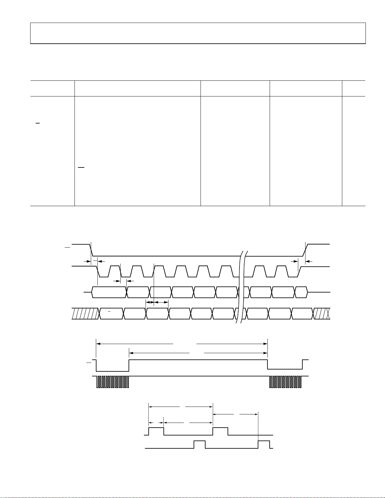
ADIS16334
TIMING SPECIFICATIONS
TA = 25°C, VCC = 5.0 V, unless otherwise noted.
Table 2.
Normal Read Burst Read1
Parameter Description Min2 Typ Max M in2 Typ Max Unit
f
Serial clock 0.01 2.0 0.01 1.0 MHz
SCLK
t
Stall period between data 9 1/f
STALL
t
Read rate 40 μs
READRATE
tCS Chip select to SCLK edge 48.8 48.8 ns
t
DOUT valid after SCLK edge 100 100 ns
DAV
t
DIN setup time before SCLK rising edge 24.4 24.4 ns
DSU
t
DIN hold time after SCLK rising edge 48.8 48.8 ns
DHD
t
, t
SCLKR
SCLK rise/fall times 5 12.5 5 12.5 ns
SCLKF
tDR, tDF DOUT rise/fall times 5 12.5 5 12.5 ns
t
SFS
t
1
high after SCLK edge
CS
Input sync positive pulse width 5 5 μs
5 5 ns
tx Input sync low time 100 100 μs
t
2
t
3
1
t
does not apply to burst read.
READRATE
2
Guaranteed by design and characterization, but not tested in production.
Input sync to data ready output 600 600 μs
Input sync period 833 833 μs
μs
SCLK
TIMING DIAGRAMS
CS
SCLK
DOUT
DIN
CS
SCLK
t
CS
1 2 3 4 5 6 15 16
t
DAV
MSB DB14
R/W A5A6 A4 A3 A2
DB13 DB12 DB10DB11 DB2 LSBDB1
t
DSU
t
DHD
D2
Figure 2. SPI Timing and Sequence
t
READRATE
t
STALL
Figure 3. Stall Time and Data Rate
t
3
t
2
t
X
SYNC
CLOCK (DIO 4)
DATA
READY
t
1
Figure 4. Input Clock Timing Diagram
Rev. A | Page 5 of 20
D1 LSB
09362-004
t
SFS
09362-002
09362-003
Page 6

ADIS16334
ABSOLUTE MAXIMUM RATINGS
Table 3.
Parameter Rating
Acceleration
Any Axis, Unpowered 2000 g
Any Axis, Powered 2000 g
VCC to GND −0.3 V to +6.0 V
Digital Input Voltage to GND −0.3 V to +5.3 V
Digital Output Voltage to GND −0.3 V to VCC + 0.3 V
Analog Input to GND −0.3 V to +3.6 V
Operating Temperature Range −40°C to +105°C
Storage Temperature Range −65°C to +125°C
1
Extended exposure to temperatures outside the specified temperature
range of −40°C to +105°C can adversely affect the accuracy of the factory
calibration. For best accuracy, store the parts within the specified operating
range of −40°C to +105°C.
2
Although the device is capable of withstanding short-term exposure to
150°C, long-term exposure threatens internal mechanical integrity.
1, 2
Stresses above those listed under Absolute Maximum Ratings
may cause permanent damage to the device. This is a stress
rating only; functional operation of the device at these or any
other conditions above those indicated in the operational
section of this specification is not implied. Exposure to absolute
maximum rating conditions for extended periods may affect
device reliability.
Table 4. Package Characteristics
Package Type θJA θ
20-Lead Module
36.5°C 16.9°C 12.5 grams
Device Weight
JC
(ML-20-1)
ESD CAUTION
Rev. A | Page 6 of 20
Page 7

ADIS16334
A
PIN CONFIGURATION AND FUNCTION DESCRIPTIONS
DIS16334
TOP VIEW
(Not to Scale)
Y-AXIS
DIO2
DIO1
VCC
GND
GND
DNC
DNC
19
20171815161314111291078563412
RST
VCC
VCC
DNC
DNC
DNC
NOTES
1. THIS REPRESENTATION DISPLAYS THE TOP VIEW WHEN THE
CONNECTO R IS VISI BLE AND FACING UP.
2. MATI NG CONNECTOR: SAMTE C CLM-110-02 O R EQUIVAL E NT.
3. DNC = DO NO T CONNECT.
GND
DIN
CS
DIO3
SCLK
DOUT
DIO4/CLKIN
09362-005
Figure 5. Pin Configuration
Z-AXIS
a
Z
g
Z
X-AXIS
a
X
a
Y
g
Y
PIN 20
PIN 2
g
X
NOTES
1. ACCELERATION (
INDICATE THE DI RECTIO N OF MO TION T HAT PRODUCES A POSITIVE
OUTPUT.
a
,
a
,
a
X
Y
Z
) AND ROTATIONAL (
g
,
g
,
g
) ARROWS
X
Y
Z
09362-006
Figure 6. Axial Orientation
Table 5. Pin Function Descriptions
Pin No. Mnemonic Type1 Description
1 DIO3 I/O Configurable Digital Input/Output.
2 DIO4/CLKIN I/O Configurable Digital Input/Output or Sync Clock Input.
3 SCLK I SPI Serial Clock.
4 DOUT O SPI Data Output. Clocks output on SCLK falling edge.
5 DIN I SPI Data Input. Clocks input on SCLK rising edge.
6
CS
I SPI Chip Select.
7, 9 DIO1, DIO2 I/O Configurable Digital Input/Output.
8
RST
I Reset.
10, 11, 12 VCC S Power Supply.
13, 14, 15 GND S Power Ground.
16, 17, 18, 19, 20 DNC N/A Do Not Connect.
1
I/O is input/output, I is input, O is output, S is supply, and N/A is not applicable.
Rev. A | Page 7 of 20
Page 8

ADIS16334
TYPICAL PERFORMANCE CHARACTERISTICS
1
10
0.1
µ +
0.01
ROOT ALLAN VARIANCE (°/sec)
0.001
0.1 1 10 100 1000 2000
T
(sec)
AU
µ
Figure 7. Gyroscope Allan Variance
µ –
09362-023
1
µ +
0.1
ROOT ALLAN VARIANCE (mg)
µ –
0.01
0.1 1 10 100 1000 2000
T
(sec)
AU
µ
Figure 8. Accelerometer Allan Variance
09362-024
Rev. A | Page 8 of 20
Page 9

ADIS16334
THEORY OF OPERATION
The ADIS16334 is a six degree of freedom (6DOF) inertial sensing
system. This sensing system collects data autonomously and
makes it available to any processor system that supports a 4-wire
serial peripheral interface (SPI).
GYROSCOPES
Angular rate sensing in the ADIS16334 begins with a MEMS
gyroscope that operates on the principle of a resonator gyro. Two
polysilicon sensing structures each contain a dither frame that
is electrostatically driven to resonance, producing the necessary
velocity element to produce a Coriolis force during angular rate.
At two of the outer extremes of each frame, orthogonal to the
dither motion, are movable fingers that are placed between
fixed pickoff fingers to form a capacitive pickoff structure that
senses Coriolis motion. The resulting signal is fed to a series of
gain and demodulation stages that produce the electrical rate
signal output. The dual-sensor design rejects external g-forces
and vibration.
ACCELEROMETERS
Acceleration sensing in the ADIS16334 starts with a MEMS
accelerometer core on each axis, which provides a linear motion-toelectrical transducer function. Tiny polysilicon springs to tether a
movable structure to a fixed frame inside the sensor core. The
springs and mass of the movable structure provide a dependable
relationship between acceleration and physical displacement
between them. The moving structure and fixed frame have
electrical plates in a balanced, differential capacitor network.
When experiencing dynamic or static acceleration, it causes a
physical deflection, which causes an imbalance in the capacitive
network. A modulation/de-modulation circuit translates the
capacitor imbalance into a representative electrical signal.
DATA SAMPLING AND PROCESSING
The analog signals from each inertial sensor feed into a mixed
signal processing circuit, which includes buffering, analog
filtering, digital sampling, digital filtering, and calibration.
CALIBRATION
The digital processing stage includes a correction function for
each accelerometer and gyroscope sensor. Each sensor within
each unit has unique correction formulas, which optimize their
bias and sensitivity accuracy over temperature and supply. The full,
6DOF characterization also enables an internal frame alignment,
which minimizes cross-axis sensitivity and simplifies frame
alignment after system installation.
USER INTERFACE
SPI Interface
The user registers manage user access to both sensor data and
configuration inputs. Each 16-bit register has its own unique bit
assignment and two addresses: one for its upper byte and one for
its lower byte. Ta b le 8 provides a memory map for each register,
along with its function and lower byte address. Each data collection
and configuration command both use the SPI, which consists of
four wires. The chip select (
and the serial clock (SCLK) synchronizes the serial data lines.
Input commands clock into the DIN pin, one bit at a time, on
the SCLK rising edge. Output data clocks out of the DOUT pin
on the SCLK falling edge. As a SPI slave device, the DOUT contents
reflect the information requested using a DIN command.
CS
) signal activates the SPI interface
MEMS
SENSOR
ADC
Figu re 9. Simplified Sensor Signal Processing Diagram
FILTERING AND
CALIBRATION
CONTROLLER
DIGITAL I/O
OUTPUT
REGISTERS
CONTROL
REGISTERS
SPI PORT
SPI SIGNALS
09362-007
Rev. A | Page 9 of 20
Page 10

ADIS16334
BASIC OPERATION
The ADIS16334 is an autonomous system that requires no user
initialization. When it has a valid power supply, it initializes itself
and starts sampling, processing, and loading sensor data into
the output registers at a sample rate of 819.2 SPS. DIO1 pulses
high after each sample cycle concludes. The SPI interface enables
simple integration with many embedded processor platforms,
as shown in Figure 10 (electrical connection) and Tab l e 6 (pin
descriptions).
VDD
SYSTEM
PROCESSOR
SPI MASTER
I/O LINES ARE COMPATIBLE WITH
3.3V OR 5V LOGIC LEVELS
SS
SCLK
MOSI
MISO
IRQ DIO1
6
3
5
4
7
Figure 10. Electrical Connection Diagram
10
CS
SCLK
DIN
DOUT
13 14 15
5V
11 12
ADIS16334
09362-008
Table 6. Generic Master Processor Pin Names and Functions
Pin Name Function
SS
Slave select
SCLK Serial clock
MOSI Master output, slave input
MISO Master input, slave output
IRQ Interrupt request
The ADIS16334 SPI interface supports full-duplex serial
communication (simultaneous transmit and receive) and uses
the bit sequence shown in Figure 14. Tabl e 7 provides a list of
the most common settings that require attention to initialize a
processor’s serial port for the ADIS16334 SPI interface.
Table 7. Generic Master Processor SPI Settings
Processor Setting Description
Master The ADIS16334 operates as a slave.
SCLK Rate ≤ 2 MHz1 Maximum serial clock rate.
SPI Mode 3 CPOL = 1 (polarity), CPHA = 1 (phase).
MSB First Mode Bit sequence.
16-Bit Mode Shift register/data length.
1
For burst read, SCLK rate ≤ 1 MHz.
READING SENSOR DATA
The ADIS16334 provides two different options for acquiring
sensor data: single register and burst register. A single register
read requires two 16-bit SPI cycles. The first cycle requests the
contents of a register using the bit assignments in Figure 14.
Bit DC7 to Bit DC0 are don’t cares for a read, and then the output
register contents follow on DOUT during the second sequence.
Figure 11 includes three single register reads in succession. In
this example, the process starts with DIN = 0x0400 to request
the contents of XGYRO_OUT, then follows with 0x0600 to
request YGYRO_OUT and 0x0800 to request ZGYRO_OUT.
Full-duplex operation enables processors to use the same 16-bit
SPI cycle to read data from DOUT while requesting the next set
of data on DIN. Figure 12 provides an example of the four SPI
signals when reading XGYRO_OUT in a repeating pattern.
DIN
0x0400 0x0600 0x0800
DOUT
CS
SCLK
DIN
DOUT
DOUT = 1111 1001 1101 1010 = 0xF9DA = –1574 LS Bs => –78.70°/sec
Figure 12. Example SPI Read, Second 16-Bit Sequence
Burst Read Function
The burst read function enables the user to read all output registers
using one command on the DIN line and shortens the stall time
between each 16-bit segment to one SCLK cycle (see Tabl e 2).
Figure 13 provides the burst read sequence of data on each SPI
signal. The sequence starts with writing 0x3E00 to DIN, followed
by each output register clocking out on DOUT, in the order in
which they appear in Tab l e 8 .
CS
SCLK
DIN
DOUT
123 8
0x3E00
XGYRO_OUT
YGYRO_OUT ZGYRO_OUT
Figure 11. SPI Read Example
DIN = 0000 0100 0000 0000 = 0x0400
DON’T CARE
XGYRO_OUT YGYRO_OUT
Figure 13. Burst Read Sequence
TEMP_OUT
09362-009
09362-011
09362-010
CS
SCLK
DIN
DOUT
R/W
A6 A5 A4 A3 A2 A1 A0 DC7 DC6 DC5 DC4 DC3 DC2 DC1 DC0
NOTES
1. THE DOUT BIT PATT E RN RE FLECTS THE ENTIRE CONTENTS O F THE REGISTER IDENTIFIE D BY [ A6: A0]
IN THE PREV IOUS 16-BIT DIN SEQUENCE W HEN R/W = 0.
2. IF R/W = 1 DURING T HE P R EV IOUS SEQU E NCE, DOUT IS NOT DEFI NE D.
Figure 14. SPI Communication Bit Sequence
Rev. A | Page 10 of 20
R/W
D0D1D2D3D4D5D6D7D8D9D10D11D12D13D14D15
A5A6
D13D14D15
9362-012
Page 11

ADIS16334
MEMORY MAP
Table 8. User Register Memory Map
Name User Access1 Flash Backup1 Address
1, 2
Default1 Register Description Bit Function1
FLASH_CNT Read only Yes 0x00 N/A Flash memory write count Table 30
Reserved N/A N/A 0x02 N/A Reserved N/A
XGYRO_OUT Read only No 0x04 N/A Output, x-axis gyroscope Table 10
YGYRO_OUT Read only No 0x06 N/A Output, y-axis gyroscope Table 10
ZGYRO_OUT Read only No 0x08 N/A Output, z-axis gyroscope Table 10
XACCL_OUT Read only No 0x0A N/A Output, x-axis accelerometer Table 12
YACCL_OUT Read only No 0x0C N/A Output, y-axis accelerometer Table 12
ZACCL_OUT Read only No 0x0E N/A Output, z-axis accelerometer Table 12
TEMP_OUT Read only No 0x10 N/A Output, internal temperature Table 14
Reserved N/A N/A 0x12 N/A Reserved N/A
Reserved N/A N/A 0x14 N/A Reserved N/A
Reserved N/A N/A 0x16 N/A Reserved N/A
Reserved N/A N/A 0x18 N/A Reserved N/A
XGYRO_OFF Read/write Yes 0x1A 0x0000 Bias correction, x-axis gyroscope Table 20
YGYRO_OFF Read/write Yes 0x1C 0x0000 Bias correction, y-axis gyroscope Table 20
ZGYRO_OFF Read/write Yes 0x1E 0x0000 Bias correction, z-axis gyroscope Table 20
XACCL_OFF Read/write Yes 0x20 0x0000 Bias correction, x-axis accelerometer Table 21
YACCL_OFF Read/write Yes 0x22 0x0000 Bias correction, y-axis accelerometer Table 21
ZACCL_OFF Read/write Yes 0x24 0x0000 Bias correction, z-axis accelerometer Table 21
ALM_MAG1 Read/write Yes 0x26 0x0000 Alarm 1, trigger polarity, threshold Table 32
ALM_MAG2 Read/write Yes 0x28 0x0000 Alarm 2, trigger polarity, threshold Table 33
ALM_SMPL1 Read/write Yes 0x2A 0x0000 Alarm 1, sample size Table 34
ALM_SMPL2 Read/write Yes 0x2C 0x0000 Alarm 2, sample size Table 34
ALM_CTRL Read/write Yes 0x2E 0x0000 Alarm, control Table 35
Reserved N/A N/A 0x30 N/A Reserved N/A
GPIO_CTRL Read/write No 0x32 0x0000 System, DIOx configuration and control Table 24
MSC_CTRL Read/write Yes 0x34 0x0006 System, data ready, self-test, calibration Table 25
SMPL_PRD Read/write Yes 0x36 0x0001 Sample rate, decimation control Table 17
SENS_AVG Read/write Yes 0x38 0x0402 Dynamic range, digital filter control Table 18
Reserved N/A N/A 0x3A N/A Reserved N/A
DIAG_STAT Read only No 0x3C 0x0000 System, status/error flags Table 26
GLOB_CMD Write only No 0x3E 0x0000 System, global commands Table 23
Reserved N/A N/A 0x40 to 0x51 N/A Reserved N/A
LOT_ID1 Read only Yes 0x52 N/A System, Lot Identification Code 1 Table 27
LOT_ID2 Read only Yes 0x54 N/A System, Lot Identification Code 2 Table 27
PROD_ID Read only Yes 0x56 0x3FCE System, product identification Table 28
SERIAL_NUM Read only Yes 0x58 N/A System, serial number Table 29
1
N/A is not applicable.
2
Each register contains two bytes. The address of the lower byte is displayed. The address of the upper byte is equal to the address of the lower byte plus 1.
Rev. A | Page 11 of 20
Page 12

ADIS16334
Y
OUTPUT DATA REGISTERS
Tabl e 9 provides a summary of the output registers. The most
significant bit in each output register provides a new data
indicator function. Every time a new data sample loads into the
output data registers, the ND bit is a 1, until a read operation
accesses the data sample. Then, this bit sets to 0, until the next
data sample loads in. The second most significant bit provides
an error/alarm indicator. This bit is equal to 1 if any error flag in
the DIAG_STAT register is equal to 1 (active).
Table 9. Output Data Register Summary
Register Address1 Function
XGYRO_OUT 0x04 Gyroscope output, x-axis
YGYRO_OUT 0x06 Gyroscope output, y-axis
ZGYRO_OUT 0x08 Gyroscope output, z-axis
XACCL_OUT 0x0A Accelerometer output, x-axis
YACCL_OUT 0x0C Accelerometer output, y-axis
ZACCL_OUT 0x0E Accelerometer output, z-axis
TEMP_OUT 0x10 Gyroscope temperature, x-axis
1
Lower byte address shown.
Gyroscopes
The output registers for the gyroscopes (angular rate of rotation)
are XGYRO_OUT, YGYRO_OUT, and ZGRYO_OUT. Table 1 0
provides the bit assignments for these registers, along with the
digital formatting for converting the digital codes into angular
rate values. Tab l e 1 1 provides several examples for converting the
14-bit, twos complement data into angular rate measurements,
and Figure 15 provides the physical/directional reference for
these sensors.
Table 10. Gyroscope Register Bit Assignments
Bit(s) Description
[15] New data, 1 = new data since last read access
[14] Error/alarm
[13:0]
Angular rate output data. Twos complement digital
format, typical sensitivity = 0.05°/sec per LSB
a
Z
Z-AXIS
Table 11. Gyroscope Data Format Examples
Rate1 Decimal Hex Binary
+300°/sec +6000 LSB 0x1770 XX01 0111 0111 0000
+0.1°/sec +2 LSB 0x0002 XX00 0000 0000 0010
+0.05°/sec +1 LSB 0x0001
0°/sec 0 LSB 0x0000
−0.05°/sec −1 LSB 0x3FFF
−0.1°/sec −2 LSB 0x3FFE
XX00 0000 0000 0001
XX00 0000 0000 0000
XX11 1111 1111 1111
XX11 1111 1111 1110
−300°/sec −6000 LSB 0x2890 XX10 1000 1001 0000
1
The numbers in the rate column reflect the default range setting, ±300°/sec.
Accelerometers
The output registers for the accelerometers are XACCL_OUT,
YACCL_OUT, and ZACCL_OUT. Table 12 provides the bit
assignments for these registers, along with the digital formatting
for converting the digital codes into angular rate values. Tabl e 1 3
provides several examples for converting the 14-bit, twos
complement data into acceleration measurements, and Figure 15
provides the physical/directional reference for these sensors.
Table 12. Accelerometer Register Bit Assignments
Bit(s) Description
[15] New data, 1 = new data since last read access
[14] Error/alarm
[13:0]
Linear acceleration output data. Twos complement
digital format, typical sensitivity = 1 mg/LSB
Table 13. Acceleration, Twos Complement Format
Acceleration Decimal Hex Binary
+5 g +5000 LSB 0x1388 XX01 0011 1000 1000
+2 mg +2 LSB 0x0002 XX00 0000 0000 0010
+1 mg +1 LSB 0x0001
0 g 0 LSB 0x0000
−1 mg −1 LSB 0x3FFF
−2 mg −2 LSB 0x3FFE
XX00 0000 0000 0001
XX00 0000 0000 0000
XX11 1111 1111 1111
XX11 1111 1111 1110
−5 g −5000 LSB 0x2C78 XX10 1100 0111 1000
g
Z
g
X
) ARROWS
X-AXIS
a
X
09362-013
-AXIS
a
Y
g
Y
PIN 20
NOTES
1. ACCELERATION (
INDICATE THE DIRECTION OF M OTION THAT PRO DUCES A POSITIVE
OUTPUT.
PIN 2
a
,
a
,
a
) AND ROTATIONAL (
X
Y
Z
Figure 15. Sensor Axes and Orientation Reference Diagram
Rev. A | Page 12 of 20
g
,
g
,
g
X
Y
Z
Page 13

ADIS16334
Internal Temperature Measurements
The TEMP_OUT register provides relative temperature
measurements for inside of the ADIS16334. This measurement
can be above ambient temperature and does not reflect external
conditions. Tabl e 14 provides the bit assignments for this register,
along with the digital data format. Tab le 1 5 provides several
examples for converting the 12-bit, offset binary data into
temperature measurements.
Table 14. Temperature Register Bit Assignments
Bit(s) Description
[15] New data, 1 = new data since last read access
[14] Error/alarm
[13:12] Not used
[11:0]
Temperature output data, offset binary format,
typical sensitivity = 0.06785°/LSB, 25°C = 0x0000
Table 15. Temperature, Twos Complement Format
Temperature Decimal Hex Binary
+105°C +1179 LSB 0x49B XXXX 0100 1001 1011
+85°C +884 LSB 0x374 XXXX 0011 0111 0100
+25.1537°C +2 LSB 0x002 XXXX 0000 0000 0010
+25.06785°C +1 LSB 0x001 XXXX 0000 0000 0001
+25°C 0 LSB 0x000 XXXX 0000 0000 0000
+24.93215°C −1 LSB 0xFFF XXXX 1111 1111 1111
+24.8643°C −2 LSB 0xFFE XXXX 1111 1111 1110
−40°C −958 LSB 0xC42 XXXX 1100 0100 0010
DEVICE CONFIGURATION
The control registers in Ta bl e 8 provide users with a variety of
configuration options. The SPI provides access to these registers,
one byte at a time, using the bit assignments in Figure 14. Each
register has 16 bits, where Bits[7:0] represent the lower address,
and Bits[15:8] represent the upper address. Figure 16 provides
an example of writing 0x03 to Address 0x37 (SMPL_PRD[15:8]),
using DIN = 0xB703. This example reduces the sample rate by
a factor of eight (see Tab l e 1 7 ).
CS
SCLK
DIN
DIN = 1011 0111 0000 0011 = 0xB703, WRITES “ 0x03” TO ADDRESS “0x37.”
Figure 16. Example SPI Write Sequence
Dual Memory Structure
Writing configuration data to a control register updates its SRAM
contents, which are volatile. After optimizing each relevant
control register setting in a system, set GLOB_CMD[3] = 1
(DIN = 0xBE08) to back these settings up in nonvolatile flash
memory. The flash backup process requires a valid power supply
level for the entire 75 ms process time. The user register map in
Tabl e 8 provides a column that indicates the registers that have
flash back-up support. A yes in the Flash Backup column indicates
that a register has a mirror location in flash and, when backed
up properly, it automatically restores itself during startup or
after a reset. Figure 17 provides a diagram of the dual-memory
structure used to manage operation and store critical user settings.
09362-014
MANUAL
FLASH
BACKUP
NONVOLATILE
FLASH MEMORY
(NO SPI ACCESS )
START-UP
RESET
Figure 17. SRAM and Flash Memory Diagram
VOLATILE
SRAM
SPI ACCESS
09362-015
Rev. A | Page 13 of 20
Page 14

ADIS16334
A
V
DIGITAL PROCESSING CONFIGURATION
Table 16. Digital Processing Registers
Register Name Address Description
SMPL_PRD 0x36 Sample rate control
SENS_AVG 0x38 Digital filtering and range control
SAMPLE RATE
The internal sampling system produces new data in the output
data registers at a rate of 819.2 SPS. The SMPL_PRD register in
Tabl e 1 7 provides two functional controls for internal sampling
and register update rates: SMPL_PRD[12:8] for decimation and
SMPL_PRD[0] for enabling the external clock option. The
decimation filter reduces the update rate, using an averaging
filter with a decimated output. These bits provide a binomial
control that divides the data rate by a factor of 2 every time this
number increases by 1. For example, set SMPL_PRD[12:8] =
00100 (DIN = 0xB704) to set the decimation factor to 16. This
reduces the update rate to 51.2 SPS and the bandwidth to 25 Hz.
Table 17. SMPL_PRD Bit Descriptions
Bit(s) Description (Default = 0x0001)
[15:13] Not used
[12:8] Average/decimation rate setting, binomial
[7:1] Not used
[0] Clock: 1 = internal (819.2 SPS), 0 = external
INPUT CLOCK CONFIGURATION
SMPL_PRD[0] provides a control for synchronizing the internal
sampling to an external clock source. Set SMPL_PRD[0] = 0
(DIN = 0xB600) to enable the external clock. See Tab le 2 and
Figure 4 for timing information.
DIGITAL FILTERING
The SENS_AVG register in Tab l e 1 8 provides user controls for
the low-pass filter. This filter contains two cascaded averaging
filters that provide a Bartlett window, FIR filter response (see
Figure 19). For example, set SENS_AVG[2:0] = 100 (DIN = 0xB804)
to set each stage to 16 taps. When used with the default sample
rate of 819.2 SPS and zero decimation (SMPL_PRD[12:8] = 00000),
this value reduces the sensor bandwidth to approximately 16 Hz.
MEMS
SENSOR
LOW-PASS
FILTER
330Hz
ADC
0
–20
–40
–60
–80
MAGNITUDE (dB)
–100
N=2
–120
–140
N=4
N=16
N=64
0.001 0.01 0.1 1
FREQUENCY (f/
f
)
S
Figure 18. Bartlett Window, FIR Filter Frequency Response
(Phase Delay = N Samples)
DYNAMIC RANGE
The SENS_AVG[10:8] bits provide three dynamic range settings
for this gyroscope. The lower dynamic range settings (±75°/sec
and ±150°/sec) limit the minimum filter tap sizes to maintain
resolution. For example, set SENS_AVG[10:8] = 010 (DIN =
0xB902) for a measurement range of ±150°/sec. Because this
setting can influence the filter settings, program SENS_AVG[10:8]
before programming SENS_AVG[2:0] if additional filtering is
required.
Table 18. SENS_AVG Bit Descriptions
Bits Description (Default = 0x0402)
[15:11] Not used
[10:8] Measurement range (sensitivity) selection
100 = ±300°/sec (default condition)
010 = ±150°/sec, filter taps ≥ 4 (Bits[2:0] ≥ 0x02)
001 = ±75°/sec, filter taps ≥ 16 (Bits[2:0] ≥ 0x04)
[7:3]
[2:0] Number of taps in each stage; value of B in N
BARTLETT WINDOW
FIR FILTER
N
B
1
x(n)
N
B
n = 1
Not used
N
B
1
x(n)
N
B
n = 1
ERAGE/
DECIMATION
FILTER
N
D
1
x(n)
N
D
n = 1
÷N
D
= 2B
B
09362-016
B = SENS_AVG[2:0]
B
N
LOW-PASS, TWO-POLE (404Hz, 757Hz)
GYROSCOPES
ACCELEROMETERS
LOW-PASS, SINGLE-POL E ( 330Hz )
Figure 19. Sampling and Frequency Response Block Diagram
CLOCK
EXTERNAL CLOCK ENABLED
BY SMPL_PRD[0] = 0
= 2
B
NB = NUMBER OFTAPS
(PER STAGE)
D = SMPL_PRD[ 12: 8 ]
D
N
= 2
D
ND = NUMBER OF TAPS
09362-017
Rev. A | Page 14 of 20
Page 15

ADIS16334
OPTIMIZING ACCURACY
The mechanical structure and assembly process of the ADIS16334
provide excellent position and alignment stability for each sensor,
even after subjected to temperature cycles, shock, vibration, and
other environmental conditions. The factory calibration includes a
dynamic characterization of each sensor’s behavior over temperature
and generates sensor-specific correction formulas. The bias
correction registers in Tab le 1 9 provide users with the ability to
address bias shifts that can result from mechanical stress. Figure 20
illustrates the summing function of each sensor’s offset correction
register.
Table 19. Registers for User Calibration
Register Address Description
XGYRO_OFF 0x1A Gyroscope bias, x-axis
YGYRO_OFF 0x1C Gyroscope bias, y-axis
ZGYRO_OFF 0x1E Gyroscope bias, z-axis
XACCL_OFF 0x20 Accelerometer bias, x-axis
YACCL_OFF 0x22 Accelerometer bias, y-axis
ZACCL_OFF 0x24 Accelerometer bias, z-axis
GLOB_CMD 0x3E Automatic calibration
X-AXIS
MEMS
GYRO
ADC
Figure 20. User Calibration, XGYRO_OFF Example
FACTORY
CALIBRATION
AND
FILTERING
XGYRO_OFF
XGYRO_OUT
09362-018
There are two options for optimizing gyroscope bias accuracy
prior to system deployment: automatic bias correction (ABC)
and manual bias correction (MBC).
AUTOMATIC BIAS CORRECTION
The ABC function provides a simple measure-and-adjust function
for the three gyroscope sensors. Set GLOB_CMD[0] = 1 (DIN =
0xBE01) to start the ABC function, which automatically performs
the following steps to correct the bias on each gyroscope:
1. Sets the output range to ±75°/sec
2. Waits for the next output register update
3. Reads the output register of the gyroscope
4. Multiplies the measurement by −1 to change its polarity
5. Writes the final value into the offset register
6. Performs a manual flash back-up function to store the
correction factor in nonvolatile flash memory
The accuracy of the bias correction depends on the internal
averaging time used for the data sample, which depends on the
decimation setting. For example, set SMPL_PRD[15:8] = 0x10
(DIN = 0xB710) to establish a decimation rate of 2
This establishes an averaging time of 80 seconds at a sample
rate of 819.2 SPS, which results in an Allan Variance of 0.006°/sec
in Figure 7.
16
, or 65536.
Rev. A | Page 15 of 20
MANUAL BIAS CORRECTION
The MBC function requires the user to collect the desired number
of samples, calculate the averages to develop bias estimates for
each gyroscope channel, and then write them into the bias offset
registers, located in Ta bl e 20 for the gyroscopes. For example,
set XGYRO_OFF = 0x1FF6 (DIN = 0x9B1F, 0x9AF6) to adjust
the XGYRO_OUT offset by −0.125°/sec (−10 LSBs). Tab l e 21
provides a manual adjustment function for the accelerometer
channels as well.
Table 20. XGYRO_OFF, YGYRO_OFF, and ZGYRO_OFF
Bit Descriptions
Bits Description (Default = 0x0000)
[15:13] Not used
[12:0]
Data bits. Twos complement, 0.0125°/sec per LSB.
Typical adjustment range = ±50°/sec.
Table 21. XACCL_OFF, YACCL_OFF, and ZACCL_OFF
Bit Descriptions
Bits Description (Default = 0x0000)
[15:12] Not used
[11:0]
Data bits. Twos complement, 1mg/LSB. Typical
adjustment range = ±2 g.
RESTORING FACTORY CALIBRATION
Set GLOB_CMD[1] = 1 (DIN = 0xBE02) to execute the factory
calibration restore function. This is a single-command function,
which resets each user calibration register to 0x0000 and all sensor
data to 0. Then, it automatically updates the flash memory within
50 ms. See Tab l e 2 3 for more information on GLOB_CMD.
POINT-OF-PERCUSSION/LINEAR-g COMPENSATION
Set MSC_CTRL[6] = 1 (DIN = 0xB446) to enable this feature
and maintain the factory-default settings for DIO1. This feature
performs a point-of-percussion translation to the point identified
in Figure 6. See Tab l e 2 5 for more information on MSC_CTRL.
Set MSC_CTRL[7] = 1 to enable internal compensation for
linear-g on the gyroscope bias.
PIN 20
PIN 2
Figure 21. Point of Percussion Reference
ORIGINALIGNMENT
REFERENCE PO INT
SEE MSC_CTRL[6].
09362-019
Page 16

ADIS16334
SYSTEM TOOLS
Tabl e 2 2 provides an overview of the control registers that provide
support for the following system level functions: global commands,
I/O control, status/error flags, device identification, MEMS selftest, and flash memory management.
Table 22. System Tool Register Addresses
Register Name Address Description
FLSH_CNT 0x00 Flash write cycle count
GPIO_CTRL 0x32 General-purpose I/O control
MSC_CTRL 0x34 Manual self-test controls
DIAG_STAT 0x3C Status, error flags
GLOB_CMD 0x3E Global commands
LOT_ID1 0x52 Lot Identification Code 1
LOT_ID2 0x54 Lot Identification Code 2
PROD_ID 0x56 Product identification
SERIAL_NUM 0x58 Serial number
Table 24. GPIO_CTRL Bit Descriptions
Bit(s) Description (Default = 0x0000)
[15:12] Not used
[11] General-Purpose I/O Line 4 (DIO4) data level
[10] General-Purpose I/O Line 3 (DIO3) data level
[9] General-Purpose I/O Line 2 (DIO2) data level
[8] General-Purpose I/O Line 1 (DIO1) data level
[7:4] Not used
[3]
[2]
[1]
[0]
General-Purpose I/O Line 4 (DIO4) direction control
(1 = output, 0 = input)
General-Purpose I/O Line 3 (DIO3) direction control
(1 = output, 0 = input)
General-Purpose I/O Line 2 (DIO2) direction control
(1 = output, 0 = input)
General-Purpose I/O Line 1 (DIO1) direction control
(1 = output, 0 = input)
GLOBAL COMMANDS
The GLOB_CMD register provides an array of single-write
commands for convenience. Setting the assigned bit in Ta bl e 23
to 1 activates each function. When the function completes, the
bit restores itself to 0. For example, clear the capture buffers by
setting GLOB_CMD[8] = 1 (DIN = 0xBF01). All of the commands
in the GLOB_CMD register require the power supply to be within
normal limits for the execution times listed in Table 2 3. Avoid
communicating with the SPI interface during these execution
times because it interrupts the process and causes data loss or
corruption.
Table 23. GLOB_CMD Bit Descriptions
Bit(s) Description Execution Time1
[15:8] Not used Not applicable
[7] Software reset 60 ms
[6:4] Not used Not applicable
[3] Register back-up to flash
[2] Not used Not applicable
[1] Factory calibration restore
[0] Gyroscope auto-null
1
This indicates the typical duration of time between the command write and
the device returning to normal operation.
General-Purpose I/O
DIO1, DIO2, DIO3, and DIO4 are configurable, general-purpose
I/O lines that serve multiple purposes according to the following
control register priority: MSC_CTRL, ALM_CTRL, and
GPIO_CTRL. For example, set GPIO_CTRL = 0x080C (DIN =
0xB308, and then 0xB20C) to configure DIO1 and DIO2 as inputs
and DIO3 and DIO4 as outputs, with DIO3 set low and DIO4
set high. In this configuration, read GPIO_CTRL (DIN = 0x3200).
The digital state of DIO1 and DIO2 is in GPIO_CTRL[9:8].
Rev. A | Page 16 of 20
Data Ready I/O Indicator
The factory default sets DIO1 as a positive data ready indicator
signal. In this configuration, the signal pulses high when all of
the output data registers have fresh data from the same sample
period. The MSC_CTRL[2:0] bits provide configuration options
for changing the default. For example, set MSC_CTRL[2:0] = 100
(DIN = 0xB404) to change the polarity of the data ready signal
on DIO1 for interrupt inputs that require negative logic inputs
for activation. See Figure 4 for an example of the data-ready timing.
Table 25. MSC_CTRL Bit Descriptions
Bit(s) Description (Default = 0x0006)
[15:12] Not used
[11]
[10]
[9:8] Not used
[7]
[6]
[5:3] Not used
[2] Data ready enable (1 = enabled, 0 = disabled)
[1] Data ready polarity (1 = active high, 0 = active low)
[0] Data ready line select (1 = DIO2, 0 = DIO1)
Memory test (cleared upon completion)
(1 = enabled, 0 = disabled)
Internal self-test enable (cleared upon completion)
(1 = enabled, 0 = disabled)
Linear acceleration bias compensation for gyroscopes
(1 = enabled, 0 = disabled)
Linear accelerometer origin alignment
(1 = enabled, 0 = disabled)
Page 17

ADIS16334
Self-Test
The self-test function allows the user to verify the mechanical
integrity of each MEMS sensor. It applies an electrostatic force
to each sensor element, which results in mechanical displacement
that simulates a response to actual motion. Ta bl e 1 lists the
expected response for each sensor and provides pass/fail criteria.
Set MSC_CTRL[10] = 1 (DIN = 0xB504) to run the internal
self-test routine, which exercises all inertial sensors, measures
each response, makes pass/fail decisions, and reports them to
error flags in the DIAG_STAT register. MSC_CTRL[10] resets
itself to 0 after completing the routine. Zero rotation provides
results that are more reliable.
Memory Test
Setting MSC_CTRL[11] = 1 (DIN = 0xB508) performs a checksum verification of the flash memory locations. The pass/fail result
is loaded into DIAG_STAT[6].
Status
The error flags provide indicator functions for common
system level issues. All of the flags are cleared (set to 0) after
each DIAG_STAT register read cycle. If an error condition
remains, the error flag returns to 1 during the next sample
cycle. The DIAG_STAT[1:0] bits do not require a read of this
register to return to 0. If the power supply voltage goes back
into range, these two flags are cleared automatically.
DEVICE IDENTIFICATION
Table 27. LOT_ID1 and LOT_ID2 Bit Descriptions
Bits Description
[15:0] Lot identification code
Table 28. PROD_ID Bit Descriptions
Bits Description
[15:0] 0x3FCE = 16,334 (decimal)
Table 29. SERIAL_NUM Bit Descriptions
Bits Description
[15:0] Serial number, lot specific
FLASH MEMORY MANAGEMENT
Set MSC_CTRL[11] = 1 (DIN = 0xB508) to run an internal
checksum test on the flash memory, which reports a pass/fail
result to DIAG_STAT[6]. The FLASH_CNT register (see Tab le 3 0)
provides a running count of flash memory write cycles. This is a
tool for managing the endurance of the flash memory. Figure 22
quantifies the relationship between data retention and junction
temperature.
Table 30. FLASH_CNT Bit Descriptions
Bits Description
[15:0] Binary counter for writing to flash memory
Table 26. DIAG_STAT Bit Descriptions
Bit(s) Description (Default = 0x0000)
[15] Z-axis accelerometer self-test failure (1 = fail, 0 = pass)
[14] Y-axis accelerometer self-test failure (1 = fail, 0 = pass)
[13] X-axis accelerometer self-test failure (1 = fail, 0 = pass)
[12] Z-axis gyroscope self-test failure (1 = fail, 0 = pass)
[11] Y-axis gyroscope self-test failure (1 = fail, 0 = pass)
[10] X-axis gyroscope self-test failure (1 = fail, 0 = pass)
[9] Alarm 2 status (1 = active, 0 = inactive)
[8] Alarm 1 status (1 = active, 0 = inactive)
[7] Not used
[6] Flash test, checksum flag (1 = fail, 0 = pass)
[5] Self-test diagnostic error flag (1 = fail, 0 = pass)
[4] Sensor overrange (1 = fail, 0 = pass)
[3] SPI communication failure (1 = fail, 0 = pass)
[2] Flash update failure (1 = fail, 0 = pass)
[1:0] Not used
600
450
300
RETENTI O N (Y ears)
150
0
30 40
55 70 85 100 125 135 150
JUNCTIONTEMPERATURE(°C)
Figure 22. Flash/EE Memory Data Retention
09362-020
Rev. A | Page 17 of 20
Page 18

ADIS16334
ALARMS
The ADIS16334 provides two independent alarms, Alarm 1 and
Alarm 2, which have a number of programmable settings. Tabl e 31
provides a list of registers for these user settings.
Table 31. Registers for Alarm Configuration
Register Address Description
ALM_MAG1 0x26 Alarm 1 trigger setting
ALM_MAG2 0x28 Alarm 2 trigger setting
ALM_SMPL1 0x2A Alarm 1 sample period
ALM_SMPL2 0x2C Alarm 2 sample period
ALM_CTRL 0x2E Alarm configuration
The ALM_CTRL register in Tabl e 35 provides data source
selection (Bits[15:8]), static/dynamic setting for each alarm
(Bits[7:6]), data source filtering (Bit[4]), and alarm indicator
signal (Bits[2:0]).
STATIC ALARM USE
The static alarms setting compares the data source selection
(ALM_CTRL[15:8]) with the values in the ALM_MAGx registers
in Tab l e 3 2 and Tabl e 3 3 . The data format in these registers
matches the format of the data selection in ALM_CTRL[15:8].
The MSB (Bit[15]) of each ALM_MAGx register establishes the
polarity for this comparison. See Tab l e 3 6 , Alarm 1, for a static
alarm configuration example.
Table 32. ALM_MAG1 Bit Descriptions
Bit(s) Description (Default = 0x0000)
[15] Trigger polarity, 1= greater than, 0 = less than
[14] Not used
[13:0]
Threshold setting; matches for format of
ALM_CTRL[11:8] output register selection
Table 33. ALM_MAG2 Bit Descriptions
Bit(s) Description (Default = 0x0000)
[15] Trigger polarity, 1= greater than, 0 = less than
[14] Not used
[13:0]
Threshold setting; matches for format of
ALM_CTRL[15:12] output register selection
DYNAMIC ALARM USE
The dynamic alarm setting monitors the data selection for a
rate-of-change comparison. The rate-of-change comparison is
represented by the magnitude in the ALM_MAGx registers over
the time represented by the number-of-samples setting in the
ALM_SMPLx registers located in Tab l e 3 4. See Ta b le 3 6, Alarm 2,
for a dynamic alarm configuration example.
Table 34. ALM_SMPL1 and ALM_SMPL2 Bit Descriptions
Bits Description (Default = 0x0000)
[15:8] Not used
[7:0] Binary, number of samples (both 0x00 and 0x01 = 1)
ALARM REPORTING
The DIAG_STAT[9:8] bits provide error flags that indicate an
alarm condition. The ALM_CTRL[2:0] bits provide controls for
a hardware indicator using DIO1 or DIO2.
Table 35. ALM_CTRL Bit Descriptions
Bit(s) Description (Default = 0x0000)
[15:12] Alarm 2 data source selection
0000 = disable
0001 = x-axis gyroscope output
0010 = y-axis gyroscope output
0011 = z-axis gyroscope output
0100 = x-axis accelerometer output
0101 = y-axis accelerometer output
0110 = z-axis accelerometer output
0111 = internal temperature output
[11:8] Alarm 1 data source selection (same as Alarm 2)
[7] Alarm 2, dynamic/static (1 = dynamic, 0 = static)
[6] Alarm 1, dynamic/static (1 = dynamic, 0 = static)
[5] Not used
[4] Data source filtering (1 = filtered, 0 = unfiltered)
[3] Not used
[2] Alarm indicator (1 = enabled, 0 = disabled)
[1] Alarm indicator active polarity (1 = high, 0 = low)
[0] Alarm output line select (1 = DIO2, 0 = DIO1)
Alarm Example
Tabl e 36 offers an example that configures Alarm 1 to trigger when
filtered ZACCL_OUT data drops below 0.7 g, and Alarm 2 to
trigger when filtered ZGYRO_OUT data changes by more than
50°/sec over a 100 ms period, or 500°/sec
helps reduce false triggers from noise and refine the accuracy
of the trigger points. The ALM_SMPL2 setting of 82 samples
provides a comparison period that is 97.7 ms for an internal
sample rate of 819.2 SPS.
Table 36. Alarm Configuration Example 1
DIN Description
0xAF36, ALM_CTRL = 0x3697.
0xAE97
0xA983,
0xA8E8
0xA702,
0xA6BC
0xAC66 ALM_SMPL2[7:0] = 0x52 (82 samples).
Alarm 2: dynamic, ΔZGYRO_OUT (Δ-time,
ALM_SMPL2) > ALM_MAG2.
Alarm 1: static, ZACCL_OUT < ALM_MAG1. Use filtered
data source for comparison. DIO2 output indicator,
positive polarity.
ALM_MAG2 = 0x83E8 (true if ΔZGYRO_OUT > 50°/sec)
50°/sec ÷ 0.05°/sec per LSB = 1000 = 0x03E8,
ALM_MAG2[15] = 1 for greater than.
ALM_MAG1 = 0x02BC (true if ZACCL_OUT < 0.7g)
0.7 g ÷ 1 mg/LSB = 700 LSB = 0x02BC,
ALM_MAG1[15] = 0 for less than.
2
. The filter setting
Rev. A | Page 18 of 20
Page 19

ADIS16334
APPLICATIONS INFORMATION
ADIS16334/PCBZ
The ADIS16334/PCBZ includes one ADIS16334BLMZ, one
interface PCB, and one interface flex. This combination of
components enables quicker installation for prototype evaluation
and algorithm development. Figure 23 provides a mechanical
design example for using these three components in a system.
15mm TO
28.40mm
20.15mm
10.07mm
ADIS16334AMLZ
NOTES
1. USE FOUR M 2 MACHINE SCREWS TO ATTACH THE ADIS1633 4BM L Z.
2. USE FOUR M 3 MACHINE SCREWS TO ATTACH THE INTERFACE PCB.
SCF-156941-01-SA
(SAMTEC P/N)
45mm
Figure 23. Physical Diagram for Mounting the ADIS16334/PCBZ
Figure 24 provides the pin assignments for the interface board,
when it is properly connected to the ADIS16334BMLZ in this
manner.
J1
RST
CS
DNC
GND
GND
VCC
1
3
5
7
9
11
2
SCLK
DOUT
4
DIN
6
8
GND
10
VCC
12
VCC
Figure 24. J1/J2 Pin Assignments for Interface PCB
DNC
DNC
GND
DNC
DNC
DIO2
23.75mm
11
12
1
2
J1
12
11
2
1
J2
INTERFACE PCB
J2
1 2
3 4
5 6
7 8
9 10
11 12
15.05mm
30.10mm
GND
DIO3
DIO4
DNC
DNC
DIO1
09362-022
09362-021
Installation
The following steps provide an example installation process for
using these three components:
• Drill and tap M2 and M3 holes in the system frame, according
to the locations in Figure 23. The distance between these
components is flexible but make sure that the hole-to-hole
distance is within the 15 mm to 45 mm range shown in the
diagram.
• Install the ADIS16334 using M2 machine screws. Use a
mounting torque of 25 inch-ounces.
• Install the interface PCB using M3 machine screws.
• Connect J1 on the interface flex to the ADIS16334BMLZ
connector.
• Connect J2 on the interface flex to J3 on the interface PCB.
Note that J2 (interface flex) has 20 pins and J3 (interface PCB)
has 24 pins. Make sure that Pin 1 on J2 (interface flex)
connects to Pin 20 on J3 (interface PCB). J3 has a Pin 1
indicator to help guide this connection.
• Connect the ADIS16334BMLZ power, ground, and SPI
signals to an embedded processor board using J1 and a
12-pin, 1 mm ribbon cable system. The following parts may
be useful in building this type of cable: 3M Part Number
152212-0100-GB (ribbon crimp connector) and 3M Part
Number 3625/12 (ribbon cable).
• Connect the ADIS16334BMLZ auxiliary I/O functions to
the embedded processor board using J2 and the same type
of ribbon cable system as J1.
The ADIS16334 does not require external capacitors for normal
operation; therefore, the interface PCB does not use the C1/C2
pads (not shown in Figure 23).
Rev. A | Page 19 of 20
Page 20

ADIS16334
OUTLINE DIMENSIONS
24.53
24.15
23.77
22.15 BSC
19.91
2.00 BSC
0.66 BSC
1.00 BSC
2.00 BSC
4.70
4.50
4.30
19.65
19.39
4.70
4.50
4.30
2.60
Ø2.40
2.20
(4 PLCS)
25.08
BSC
30.40
BSC
33.08
32.70
32.32
2.96 BSC
10.90
10.60
10.30
2.96
2.70
2.44
10.23
BSC
6.09
5.83
5.57
7.58
BSC
TOP VIEW
18.59
18.33
18.07
1.00 BSC
PITCH
END VIEW
21.85 BSC
2.30 BSC
(2 PLCS)
3.12
2.86
2.60
5.96
5.70
5.44
01-18-2011-B
Figure 25. 20-Lead Module with Connector Interface
(ML-20-1)
Dimensions shown in millimeters
ORDERING GUIDE
Model1 Temperature Range Package Description Package Option
ADIS16334BMLZ −40°C to +105°C 20-Lead Module with Connector Interface ML-20-1
ADIS16334/PCBZ Evaluation Board
1
Z = RoHS Compliant Part.
©2011 Analog Devices, Inc. All rights reserved. Trademarks and
registered trademarks are the property of their respective owners.
D09362-0-6/11(A)
Rev. A | Page 20 of 20
 Loading...