

Page 1
High-Accuracy, Dual-Axis
Digital Inclinometer and Accelerometer
FEATURES
Dual-mode inclinometer system
Dual-axis, horizontal operation, ±90°
Single-axis, vertical operation, ±180°
High accuracy, 0.1°
14-bit digital inclination data, 0.025° resolution
14-bit digital acceleration data, 0.244 mg resolution
±1.7 g accelerometer measurement range
12-bit digital temperature sensor output
Digitally controlled bias calibration
Digitally controlled sample rate
Digitally controlled frequency response
Dual alarm settings with rate/threshold limits
Auxiliary digital I/O
Digitally activated self-test
Digitally activated low power mode
SPI-compatible serial interface
Auxiliary 12-bit ADC input and DAC output
Single-supply operation: 3.0 V to 3.6 V
3500 g powered shock survivability
VDD
GND
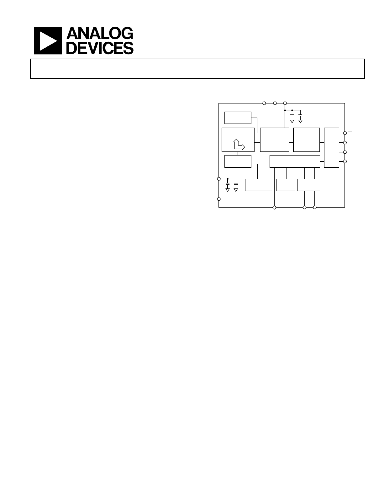
FUNCTIONAL BLOCK DIAGRAM
AUX
AUX
TEMPERATURE
SENSOR
DUAL-AXIS
ACCELEROMETER
SELF-TEST
MANAGEMENT
ADC
POWER
VREF
DAC
SIGNAL
CONDITIONI NG
AND
CONVERSION
RST DIO1 DIO2
Figure 1.
ALARMS
CALIBRATION
PROCESSING
DIGITAL
CONTROL
DIGIT AL
AUXILIARY
ADIS16209
ADIS16209
AND
SPI
PORT
I/O
CS
SCLK
DIN
DOUT
07096-001
APPLICATIONS
Platform control, stabilization, and alignment
Tilt sensing, inclinometers, leveling
Motion/position measurement
Monitor/alarm devices (security, medical, safety)
Navigation
GENERAL DESCRIPTION
The ADIS16209 is a high-accuracy, digital inclinometer that
accommodates both single axis (±180°) and dual-axis (±
peration. The standard supply voltage (3.3 V) and serial
o
peripheral interface (SPI) serial interface enable simple
integration into most industrial system designs. A simple
internal register structure handles all output data and
configuration features. This includes access to the following
output data: calibrated acceleration, accurate incline angles,
power supply, internal temperature, auxiliary analog and digital
input signals, diagnostic error flags, and programmable alarm
conditions.
90°)
Configurable operating parameters include sample rate,
power management, digital filtering, auxiliary analog and
digital output, offset/null adjustment, and self-test for sensor
mechanical structure.
The ADIS16209 is available in a 9.2 mm × 9.2 mm × 3.9 mm
LGA package that operates over a temperature range of −40°C
to +125°C. It can be attached using standard RoHS-compliant
solder reflow processes.
Rev. 0
Information furnished by Analog Devices is believed to be accurate and reliable. However, no
responsibility is assumed by Analog Devices for its use, nor for any infringements of patents or other
rights of third parties that may result from its use. Specifications subject to change without notice. No
license is granted by implication or otherwise under any patent or patent rights of Analog Devices.
Trademarks and registered trademarks are the property of their respective owners.
One Technology Way, P.O. Box 9106, Norwood, MA 02062-9106, U.S.A.
Tel: 781.329.4700 www.analog.com
Fax: 781.461.3113 ©2008 Analog Devices, Inc. All rights reserved.
Page 2

ADIS16209
TABLE OF CONTENTS
Features .............................................................................................. 1
Applications ....................................................................................... 1
Functional Block Diagram .............................................................. 1
General Description ......................................................................... 1
Revision History ............................................................................... 2
Specifications ..................................................................................... 3
Timing Specifications .................................................................. 5
Timing Diagrams .......................................................................... 5
Absolute Maximum Ratings ............................................................ 6
Thermal Resistance ...................................................................... 6
ESD Caution .................................................................................. 6
REVISION HISTORY
3/08—Revison 0: Initial Version
Pin Configuration and Function Descriptions ..............................7
Recommended Pad Geometry ....................................................7
Typical Performance Characteristics ..............................................8
Theory of Operation ...................................................................... 10
Basic Operation .............................................................................. 11
Output Data Registers ............................................................... 12
Operation Control Registers ..................................................... 12
Calibration Registers .................................................................. 14
Alarm Registers .......................................................................... 14
Outline Dimensions ....................................................................... 16
Ordering Guide .......................................................................... 16
Rev. 0 | Page 2 of 16
Page 3

ADIS16209
SPECIFICATIONS
TA = 25°C, VDD = 3.3 V, tilt = 0°, unless otherwise noted.
Table 1.
Parameter Conditions Min Typ Max Unit
HORIZONTAL INCLINE Each axis
Input Range ±90 Degrees
Relative Accuracy ±30° from horizon, AVG_CNT = 0x08 ±0.1 Degrees
Sensitivity ±30° from horizon 0.025 °/LSB
VERTICAL ROTATION Rotational plane within ±30 degrees of vertical
Input Range −180 +180 Degrees
Relative Accuracy 360° of rotation ±0.25 Degrees
Sensitivity −40°C to +85°C 0.025 °/LSB
ACCELEROMETER Each axis
Input Range
Nonlinearity
Alignment Error X sensor to Y sensor ±0.1 Degrees
Cross Axis Sensitivity ±2 %
Sensitivity −40°C to +85°C, VDD = 3.0 V to 3.6 V 0.243 0.244 0.245 mg/LSB
ACCELEROMETER NOISE PERFORMANCE
Output Noise AVG_CNT = 0x00 1.7 mg rms
Noise Density AVG_CNT = 0x00 0.19 mg/√Hz rms
ACCELEROMETER FREQUENCY RESPONSE
Sensor Bandwidth 50 Hz
Sensor Resonant Frequency 5.5 kHz
ACCELEROMETER SELF-TEST STATE
Output Change When Active At 25°C 706 1343 1973 LSB
TEMPERATURE SENSOR
Output at 25°C 1278 LSB
Scale Factor −0.47 °C/LSB
ADC INPUT
Resolution 12 Bits
Integral Nonlinearity (INL) ±2 LSB
Differential Nonlinearity (DNL) ±1 LSB
Offset Error ±4 LSB
Gain Error ±2 LSB
Input Range 0 2.5 V
Input Capacitance During acquisition 20 pF
ON-CHIP VOLTAGE REFERENCE 2.5 V
Accuracy At 25°C −10 +10 mV
Reference Temperature Coefficient ±40 ppm/oC
Output Impedance 70 Ω
DAC OUTPUT 5 kΩ/100 pF to GND
Resolution 12 Bits
Relative Accuracy For Code 101 to Code 4095 4 LSB
Differential Nonlinearity 1 LSB
Offset Error ±5 mV
Gain Error ±0.5 %
Output Range 0 to 2.5 V
Output Impedance 2 Ω
Output Settling Time 10 µs
1
1
2
25°C ±1.7
% of full scale ±0.1 ±0.2 %
g
Rev. 0 | Page 3 of 16
Page 4

ADIS16209
Parameter Conditions Min Typ Max Unit
LOGIC INPUTS
Input High Voltage, V
Input Low Voltage, V
Logic 1 Input High Current, I
Logic 0 Input Low Current, I
All except
RST
RST
3
Input Capacitance, CIN 10 pF
DIGITAL OUTPUTS
Output High Voltage, VOH I
Output Low Voltage, VOL I
SLEEP TIMER
Timeout Period
START-UP TIME
5
Power-On Fast mode, SMPL_PRD ≤ 0x07 150 ms
Normal mode, SMPL_PRD ≥ 0x08 190 ms
Reset Recovery Fast mode, SMPL_PRD ≤ 0x07 30 ms
Normal mode, SMPL_PRD ≥ 0x08 70 ms
Sleep Mode Recovery 2.5 ms
FLASH MEMORY
Endurance
6
Data Retention
CONVERSION RATE SETTING 1.04 2731 SPS
POWER SUPPLY
Operating Voltage Range 3.0 3.3 3.6 V
Power Supply Current Normal mode, SMPL_PRD ≥ 0x08 11 14 mA
Fast mode, SMPL_PRD ≤ 0x07 36 42 mA
Sleep mode, −40°C to +85°C 140 350 µA
1
Guaranteed by iMEMS® packaged part testing, design, and/or characterization.
2
Self-test response changes as the square of VDD.
3
RST
The
pin has an internal pull-up.
4
Guaranteed by design.
5
The times presented in this section do not include the sensor’s transient response time, which is associated with a 50 Hz single-pole system. System accuracy goals
should be given consideration when determining the amount of time it takes to start acquiring accurate readings. These times do not include the time it takes to
arrive at thermal stability, which can also introduce transient errors.
6
Endurance is qualified as per JEDEC Standard 22 Method A117 and measured at −40°C, +25°C, +85°C, and +125°C.
7
Retention lifetime equivalent at junction temperature (TJ) 55°C as per JEDEC Standard 22 Method A117. Retention lifetime decreases with junction temperature.
2.0 V
INH
0.8 V
INL
CS
For
signal when used to wake up from sleep mode
VIH = 3.3 V ±0.2 ±10 µA
INH
V
INL
= 0 V
IL
−40 −60 A
0.55 V
−1 mA
= 1.6 mA 2.4 V
SOURCE
= 1.6 mA 0.4 V
SINK
4
0.5 128 Seconds
Time until data is available
20,000 Cycles
7
TJ = 85°C 20 Years
Rev. 0 | Page 4 of 16
Page 5
ADIS16209
K
TIMING SPECIFICATIONS
TA = 25°C, VDD = 3.3 V, tilt = 0°, unless otherwise noted.
Table 2.
Parameter Description Min1 Typ Max Unit
f
Fast mode, SMPL_PRD ≤ 0x07 (fS ≥ 546 Hz)2 0.01 2.5 MHz
SCLK
Normal mode, SMPL_PRD ≥ 0x08 (fS ≤ 482 Hz)2 0.01 1.0 MHz
t
Chip select period, fast mode, SMPL_PRD ≤ 0x07 (fS ≥ 546 Hz)2 40 s
DATARATE
tCS Chip select to clock edge 48.8 ns
t
Data output valid after SCLK edge 100 ns
DAV
t
Data input setup time before SCLK rising edge 24.4 ns
DSU
t
Data input hold time after SCLK rising edge 48.8 ns
DHD
tDF Data output fall time 5 12.5 ns
tDR Data output rise time 5 12.5 ns
t
SFS
1
Guaranteed by design, not tested.
2
Note that fS means internal sample rate.
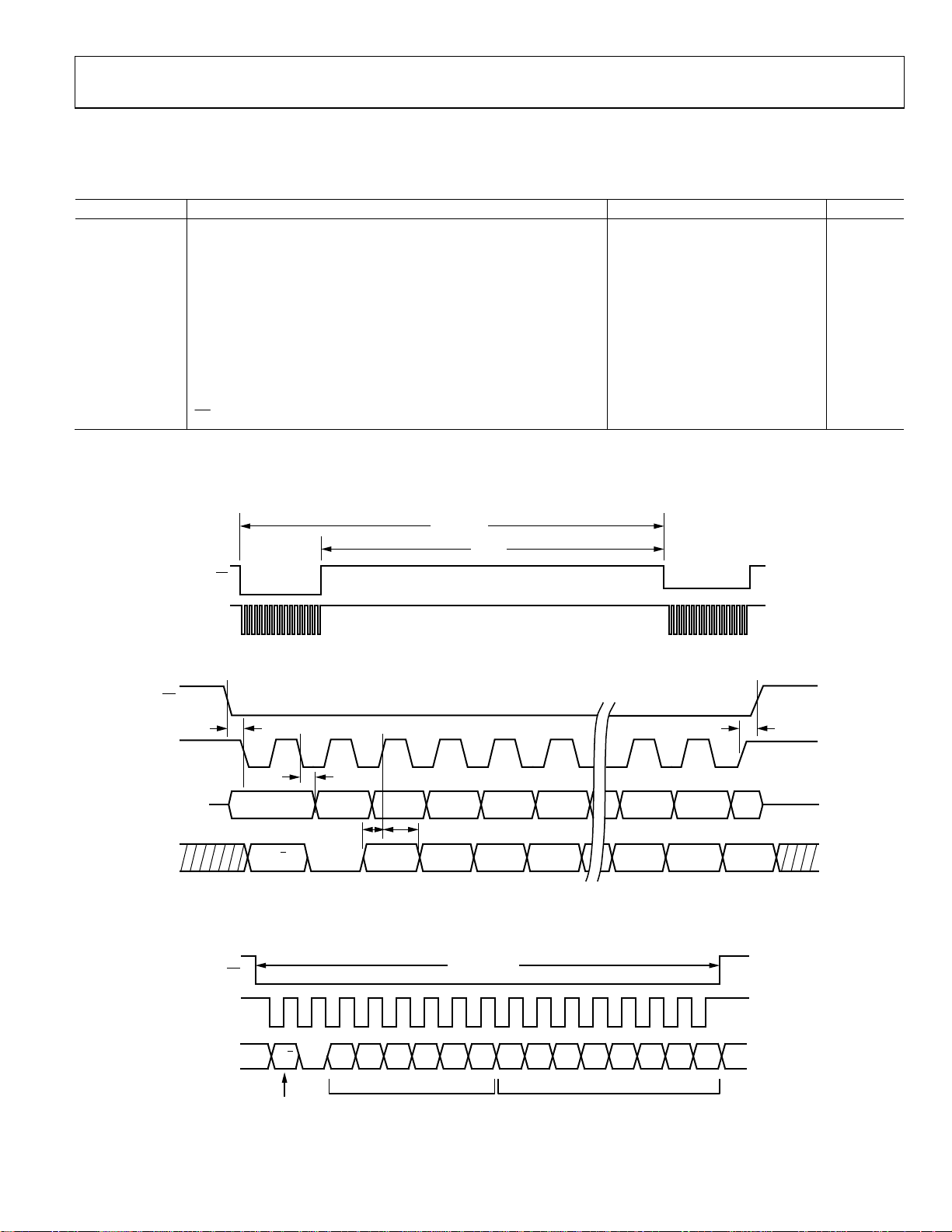
TIMING DIAGRAMS
Chip select period, normal mode, SMPL_PRD ≥ 0x08 (fS ≤ 482 Hz)2 100 s
high after SCLK edge
CS
t
DATARATE
t
STALL
5 ns
CS
SCLK
t
=
t
– 16/
STALL
DATARATE
f
SCLK
07096-002
Figure 2. SPI Chip Select Timing
CS
SCLK
DOUT
DIN
t
CS
1 2 3 4 5 6 15 16
t
DAV
MSB DB14
W/R A5 A4 A3 A2
DB13 DB12 DB10DB11 DB2 LSBDB1
t
DSU
t
DHD
D2
D1 L SB
t
SFS
07096-003
Figure 3. SPI Timing
(Utilizing SPI Settings Typically Identified as Phase = 1, Polarity = 1)
CS
SCL
DATA FRAME
DIN
W/R A5 A4 A3 A2 A1 A0 DC7 DC6 DC5 DC4 DC3 DC2 DC1 DC0
WRITE = 1
READ = 0
REGISTER ADDRESS DATA FOR WRITE COMMANDS
DON’T CARE FO R READ COMMANDS
07096-004
Figure 4. DIN Bit Sequence
Rev. 0 | Page 5 of 16
Page 6

ADIS16209
ABSOLUTE MAXIMUM RATINGS
Table 3.
Parameter Rating
Acceleration (Any Axis, Unpowered) 3500 g
Acceleration (Any Axis, Powered) 3500 g
VDD to GND −0.3 V to +7.0 V
Digital Input/Output Voltage to GND −0.3 V to +5.5 V
Analog Inputs to GND −0.3 to VDD + 0.3 V
Analog Inputs to GND −0.3 to VDD + 0.3 V
Operating Temperature Range −40°C to +125°C
Storage Temperature Range −65°C to +150°C
Stresses above those listed under Absolute Maximum Ratings
may cause permanent damage to the device. This is a stress
rating only; functional operation of the device at these or any
other conditions above those indicated in the operational
section of this specification is not implied. Exposure to absolute
maximum rating conditions for extended periods may affect
device reliability.
THERMAL RESISTANCE
Table 4. Package Characteristics
Package Type θJA θ
16-Terminal LGA 250°C/W 25°C/W 0.6 grams
Device Weight
JC
ESD CAUTION
Rev. 0 | Page 6 of 16
Page 7

ADIS16209
2
PIN CONFIGURATION AND FUNCTION DESCRIPTIONS
F
AUX ADC
VRE
GND
16 15 14 13
A
SCLK
DOUT
DIN
CS
NOTES
1. NC = NO CONNECT.
. THIS IS NOT AN ACTUAL TO P VIEW, BECAUSE THE PINS ARE NOT VIS IBLE FROM THE TOP. THIS IS
A LAYOUT VI EW, WHI CH REPRESENTS T HE PIN CONFI GURATIO N, IF THE PACKAGE IS LOOKED
THROUGH FRO M THE TOP . THIS CO NFIGURATI ON IS PRO VIDED FOR PCB L AYOUT PURPO SES.
Y
A
X
PIN 1
INDICATO R
ADIS16209
TOP
LOOK THRO UGH
VIEW
(Not to Scale)
4 3 2 1
5 6 7 8
DIO2
DIO1
Figure 5. Pin Configuration
VDD
AUX DAC
NC
NC
9 10 11 12
RST
NC
NC
07096-005
Table 5. Pin Function Descriptions
Pin No. Mnemonic Type
1
Description
1 SCLK I SPI, Serial Clock.
2 DOUT O SPI, Data Output.
3 DIN I SPI, Data Input.
4
CS
I SPI, Chip Select.
5, 6 DIO1, DIO2 I/O Digital Input/Output Pins.
7, 8, 10, 11 NC N/A No Connect.
9
RST
I Reset, Active Low.
12 AUX DAC O Auxiliary DAC Output.
13 VDD S Power Supply, 3.3 V.
14 AUX ADC I Auxiliary ADC Input.
15 VREF O Precision Reference.
16 GND S Ground.
1
S = supply; O = output; I = input.
RECOMMENDED PAD GEOMETRY
4.1865
8×
0.670
12×
8.373
2×
5.391
4×
2.6955
8×
0.500
1.127
16×
9.2mm × 9.2mm S TACKED LGA PACKAGE
16×
07096-006
Figure 6. Example of a Pad Layout
Rev. 0 | Page 7 of 16
Page 8

ADIS16209
TYPICAL PERFORMANCE CHARACTERISTICS
0.20
0.15
0.10
0.05
0
–0.05
ERROR (Degrees)
–0.10
–0.15
–0.20
–40 –30 –20 –10 0 10 20 30 40
INCLINATI ON ANGLE (Degrees)
MAXIMUM
INCLINE
ERROR
Figure 7. Horizontal Inclination Error (8 Parts), Autonull at Horizontal
Position, Stable Temperature, 3.3 V
0.3
07096-018
0.25
0.20
0.15
0.10
0.05
0
–0.05
ERROR (Degrees)
–0.10
–0.15
–0.20
–0.25
0 100 200 300 400
ROTATIO NAL ANGLE (Degrees)
Figure 10. Vertical Mode Rotational Error (8 parts), 25°C, 3.3 V
0.3
07096-021
0.2
0.1
0
–0.1
ERROR (Degrees)
–0.2
–0.3
–60 –4 0 – 20 0 20 40 60 80 100
TEMPERATURE (°C)
07096-019
Figure 8. Maximum Incline Error over a ±30° Incline Range (8 Parts) over
Temperature, Autonull at Horizontal Position, 25°C, 3.3 V
0.15
0.10
0.05
0
–0.05
ERROR (Degrees)
–0.10
–0.15
0.2
0.1
0
–0.1
–0.2
ERROR (Degrees)
–0.3
–0.4
–0.5
–60 –40 –20 0 20 40 60 80 100
TEMPERATURE ( °C)
Figure 11. Vertical Mode Error (8 Parts) vs. Temperature, 0° to 360°, 3.3 V
0.3
0.2
0.1
0
–0.1
–0.2
ERROR (Degrees)
–0.3
–0.4
07096-022
–0.20
3.0 3.3 3.6
SUPPLY VOLTAGE (V)
Figure 9. Maximum Incline Error over a ±30° Incline Range (8 Parts) over
Supply Voltage, Autonull Horizontal Position, 25°C, 3.3 V
07096-020
Rev. 0 | Page 8 of 16
–0.5
3.0 3.3 3.6
SUPPLY VOLTAGE (V)
07096-023
Figure 12. Vertical Mode Error (8 Parts) vs. Supply Voltage, 0° to 360°, 25°C
Page 9

ADIS16209
30
25
VDD = 3.0V, 3. 3V, 3.6V
TEMP = –40°C, +25°C, +85°C
3.5
3.0
20
15
10
5
PERCENTAGE O F POPULAT ION (%)
0
–0.50 –0. 38 –0.26 –0.14 –0. 02 0.10 0.22 0.34 0.46
SENSITIV ITY ERROR (%)
Figure 13. Accelerometer Output Sensitivity Error Distribution
20
18
16
14
12
10
8
6
4
PERCENTAGE O F POPULAT ION (%)
2
0
–6.0 –4.4 –2.8 –1.2 0.4 2.0 3.6 5.2
BIAS ERROR (mg)
VDD = 3.0V, 3. 3V, 3.6V
TEMP = –40 °C, +25°C, +85°C
Figure 14. Accelerometer Output Bias Error Distribution
2.5
2.0
1.5
ERROR (Degrees)
1.0
0.5
0
0 102030405060708090
07096-013
OFF-VE RTICAL T ILT (Deg rees)
7096-015
Figure 15. Error vs. Off-Vertical Tilt, 25°C, 3.3 V
07096-014
Rev. 0 | Page 9 of 16
Page 10

ADIS16209
G
G
THEORY OF OPERATION
The ADIS16209 tilt sensing system uses gravity as its only
stimulus, and a MEMS accelerometer as its sensing element.
MEMS accelerometers typically employ a tiny, spring-loaded
structure that is interlaced with a fixed pick-off finger structure.
The spring constant of the floating structure determines how
far it moves when subjected to a force. This structure responds
to dynamic forces associated with acceleration and to static
forces, such as gravity.
Figure 16 and Figure 17 illustrate how the accelerometer
responds to gravity, according to its orientation, with respect
to gravity. Figure 16 displays the configuration for the incline
angle outputs, and Figure 17 displays the configuration used
for the rotational angle position. This configuration provides
greater measurement range than a single axis. The ADIS16209
incorporates the signal processing circuit that converts acceleration into an incline angle, and corrects for several known error
sources that would otherwise degrade the accuracy level.
0° TIL T
LEVEL PLANE
POSITIVE
X AXIS TILT
DIRECTION
58
4
Y AXIS Y AXIS
POSITIVE
Y AXIS TILT
DIRECTION
4
16
1
XINCL_OUT = 0°
YINCL_OUT = 0°
13
12
9
85
Figure 18. Horizontal Incline Angle Orientation
POSITIVE DIRECTION
1
9
1316
0° ≤ XINCL_OUT ≤ 90°
YINCL_OUT = 0°
RAVITY = 1g
Figure 16. Single-Axis Tilt Theory Diagram
RAVITY = 1g
Figure 17. Dual-Axis Tilt Theory Diagram
12
4
θ
x
a
x
θ
x
HORIZON
a
y
θ
x
a
x
θ
x
HORIZON
16
1
5
13
12
9
8
XINCL_OUT = 0°
0° ≤ YINCL_OUT ≤ 90°
07096-007
07096-008
X AXISX AXIS
07096-011
1
6
2
0
9
1
6
2
0
16209
ROT_OUT = 0°
9
90° ≤ ROT_OUT ≤ 180°
–180° ≤ ROT_OUT ≤ –90°
07096-012
Figure 19. Vertical Angle Orientation
Rev. 0 | Page 10 of 16
Page 11

ADIS16209
BASIC OPERATION
The ADIS16209 requires only power/ground and SPI connections. The SPI is simple to hook up and is supported by many
common digital hardware platforms. Figure 20 provides a
simple hook-up diagram, while Table 2, Figure 2, and Figure 3
provide timing and bit assignments. Figure 4 provides the bit
sequence for accessing the register memory structure. Each
function within the ADIS16209 has its own 16-bit, 2-byte register. Each byte has its own unique, 6-bit address. Note that
all 16 SCLK cycles are required for the DIN bit sequence to
configure the output for the next data frame. The ADIS16209
supports full duplex mode operation. Table 6 provides the
entire user register map for the ADIS16209. For each register,
the lower bytes address is given. For those registers that have
two bytes, the upper bytes address is simply the lower bytes
Many of the configuration registers have also been assigned
mirror locations in the flash memory, which effectively provides
them with a backup storage function. To assure the backup of
these registers, the COMMAND register provides an initiation
bit for manual flash updates. The ENDURANCE register
provides a running count of these events.
ADIS16209
CS
SCLK
DIN
DOUT
Figure 20. Typical SPI Hook-up
address, incremented by 0x01.
Table 6. User Register Map
Name R/W Flash Backup Address Size (Bytes) Function Reference
ENDURANCE R Yes 0x00 2 Diagnostics, flash write counter (16-bit binary)
SUPPLY_OUT R No 0x02 2 Output, power supply Table 7
XACCL_OUT R No 0x04 2 Output, x-axis acceleration Table 7
YACCL_OUT R No 0x06 2 Output, y-axis acceleration Table 7
AUX_ADC R No 0x08 2 Output, auxiliary ADC Table 7
TEMP_OUT R No 0x0A 2 Output, temperature Table 7
XINCL_OUT R No 0x0C 2 Output, ±90° x-axis inclination Table 7
YINCL_OUT R No 0x0E 2 Output, ±90° y-axis inclination Table 7
ROT_OUT R No 0x10 2 Output, ±180° vertical rotational position Table 7
XACCL_NULL R/W Yes 0x12 2 Calibration, x-axis acceleration offset null Table 16
YACCL_NULL R/W Yes 0x14 2 Calibration, y-axis acceleration offset null Table 16
XINCL_NULL R/W Yes 0x16 2 Calibration, x-axis inclination offset null Table 17
YINCL_NULL R/W Yes 0x18 2 Calibration, y-axis inclination offset null Table 17
ROT_NULL R/W Yes 0x1A 2 Calibration, vertical rotation offset null Table 17
0x1C to 0x1F 4 Reserved, do not write to these locations
ALM_MAG1 R/W Yes 0x20 2 Alarm 1, amplitude threshold Table 18
ALM_MAG2 R/W Yes 0x22 2 Alarm 2, amplitude threshold Table 18
ALM_SMPL1 R/W Yes 0x24 2 Alarm 1, sample period Table 19
ALM_SMPL2 R/W Yes 0x26 2 Alarm 2, sample period Table 19
ALM_CTRL R/W Yes 0x28 2 Alarm, source control register Table 20
No 0x2A to 0x2F 6 Reserved
AUX_DAC R/W No 0x30 2 Auxiliary DAC data Table 14
GPIO_CTRL R/W No 0x32 2 Operation, digital I/O configuration and data Table 13
MSC_CTRL R/W No 0x34 2 Operation, data-ready and self-test control Table 12
SMPL_PRD R/W Yes 0x36 2 Operation, sample rate configuration Table 8
AVG_CNT R/W Yes 0x38 2 Operation, filter configuration Table 10
SLP_CNT W Yes 0x3A 2 Operation, sleep mode control Table 9
STATUS R No 0x3C 2 Diagnostics, system status register Table 21
COMMAND W No 0x3E 2 Operation, system command register Table 15
EMBEDDED
PROCESSOR/
DSP/FPGA
PF
SCK
MOSI
MISO
07096-009
Rev. 0 | Page 11 of 16
Page 12

ADIS16209
OUTPUT DATA REGISTERS
Tabl e 7 provides the data configuration for each output data
register in the ADIS16209. Starting with the MSB of the upper
byte, each output data register has the following bit sequence:
new data (ND) flag, error/alarm (EA) flag, followed by 14 data
bits. The data bits are LSB-justified and, in the case of the 12-bit
data formats, the remaining two bits are not used. The ND flag
indicates that unread data resides in the output data registers.
This flag clears and returns to 0 during an output register read
sequence. It returns to 1 after the next internal sample update
cycle completes. The EA flag indicates an error condition. The
STATUS register contains all of the error flags and provides the
ability to investigate root cause.
Table 7. Output Data Register Formats
Register Bits Format Scale1
SUPPLY_OUT 14 Binary, 3.3 V = 0x2A3D 0.30518 mV
XACCL_OUT 14 Twos complement 0.24414 mg
YACCL_OUT 14 Twos complement 0.24414 mg
AUX_ADC 12 Binary, 2 V = 0x0CCC 0.6105 mV
TEMP_OUT 12 Binary, 25°C = 0x04FE −0.47°C
XINCL_OUT2 14 Twos complement 0.025°
YINCL_OUT2 14 Twos complement 0.025°
ROT_OUT3 14 Twos complement 0.025°
1
Scale denotes quantity per LSB.
2
Range is −90° to +90°.
3
Range is −180° to +179.975°.
of 68%. The two different modes of operation offer a systemlevel trade-off between performance (sample rate, serial transfer
rate) and power dissipation.
Power Management
In addition to offering two different performance modes for
power optimization, the ADIS16209 offers a programmable
shutdown period that the SLP_CNT register controls.
Table 9. SLP_CNT Bit Descriptions
Bit Description (Default = 0x0000)
15:8 Not used
7:0 Data bits, 0.5 seconds/LSB
For example, writing 0x08 to the SLP_CNT register places the
ADIS16209 into sleep mode for 4 seconds. The only way to stop
this process is to remove power or reset the device.
Digital Filtering
The AVG_CNT register controls the moving average digital filter,
which determines the size of the moving average filter, in eight
power-of-two step sizes (that is, 2
M
= 1, 2, 4, 16, 32, 64, 128, and
256). Filter setup requires one simple step: write the appropriate
M factor to the assigned bits in the AVG_CNT register.
Table 10. AVG_CNT Bit Descriptions
Bit Description (Default = 0x0004)
15:4 Not used
3:0 Power-of-two step size, maximum binary value = 1000
OPERATION CONTROL REGISTERS
Internal Sample Rate
The SMPL_PRD register controls the ADIS16209 internal sample
rate and has two parts: a selectable time base and a multiplier. The
following relationship produces the sample rate:
= tB × NS + 122.07μs
t
S
Table 8. SMPL_PRD Bit Descriptions
Bit Description (Default = 0x0004)
15:8 Not used
7 Time base (tB)
0 = 244.14 µs, 1 = 7.568 ms
6:0 Increment setting (NS)
An example calculation of the default sample period follows:
SMPL_PRD = 0x01, B7 − B0 = 00000001
B7 = 0 → t
t
= tB × NS + 122.07μs = 244.14 × 1 + 122.07 = 366.21 μs
S
f
= 1∕tS = 2731 SPS
S
The sample rate setting has a direct impact on the SPI data
rate capability. For sample rates ≥546 SPS, the SPI SCLK can
run at a rate up to 2.5 MHz. For sample rates <546 SPS, the SPI
SCLK can run at a rate up to 1 MHz. The sample rate setting
also affects power dissipation. When the sample rate is set to
<546 SPS, power dissipation typically reduces by a factor
= 244.14 μs, B6…B0 = 000000001 → NS = 1
B
The following equation offers a frequency response relationship
for this filter:
)sin(
tfN
×××π
S
)(
fH
=
A
20
0
–20
–40
MAGNITUDE (d B)
–60
–80
–100
0.001 0. 01 0.1
Figure 21. Frequency Response—Moving Average Filter
××π×
tfN
S
N = 128
)sin(
N = 4
N = 16
f/f
S
07096-010
Rev. 0 | Page 12 of 16
Page 13

ADIS16209
Digital I/O Lines
The ADIS16209 provides two, general purpose, digital
input/output lines that have several configuration options.
Table 11. Digital I/O Line Configuration Registers
Function [Priority] Register
Data-Ready I/O Indicator [1] MSC_CTRL
Alarm Indicator [2] ALM_CTRL
General-Purpose I/O Configuration [3] GPIO_CTRL
General-Purpose I/O Line Communication GPIO_CTRL
Table 13. GPIO_CTRL Bit Descriptions
Bit Description (Default = 0x0000)
15:10 Not used
9 General-Purpose I/O Line 2 data
8 General-Purpose I/O Line 1 data
7:2 Not used
1 General-Purpose I/O Line 2, data direction control
1 = output, 0 = input
0 General-Purpose I/O Line 1, data direction control
1 = output, 0 = input
Data-Ready I/O Indicator
The MSC_CTRL register provides controls for a data-ready
function. For example, writing 0x05 to this register enables this
function and establishes DIO2 as an active-low, data-ready line.
The duty cycle is 25% (±10% tolerance).
Table 12. MSC_CTRL Bit Descriptions
Bit Description (Default = 0x0000)
15:11 Not used
10 Self-test at power-on: 1 = disabled, 0 = enabled
9 Not used
8 Self-test enable (temporary, bit is volatile)
1 = enabled, 0 = disabled
7:3 Not used
2 Data-ready enable: 1 = enabled, 0 = disabled
1 Data-ready polarity: 1 = active high, 0 = active low
0 Data-ready line select: 1 = DIO2, 0 = DIO1
Self-Test
Self-test exercises the mechanical structure of the sensor and
provides a simple method for verifying the operation of the
entire sensor signal conditioning circuit. There are two different
self-test options: startup and manual. If either of these self-tests
results in a failure, the self-test error flag, located in the STATUS
register, sets to 1. The manual self-test option results in a
repeating pattern, until the bit is set back to 0. While in the
manual self-test loop, SMPL_PRD and AVG_CNT cannot be
changed. See Ta ble 1 2 for the appropriate MSC_CTRL bit
designations.
General Purpose I/O
The GPIO_CTRL register controls the direction and data of the
general-purpose digital lines, DIO1 and DIO2. For example,
writing a 0x02 to the GPIO_CTRL register sets DIO2 as an
output line and DIO1 as an input line. Reading the data bits in
GPIO_CTRL reveals the line logic level.
Auxiliary DAC
The auxiliary DAC provides a 12-bit level adjustment function.
The AUX_DAC register controls the operation of the auxiliary
DAC function, which is useful for systems that require analog
level controls. It offers a rail-to-rail buffered output that has a
range of 0 V to 2.5 V. The DAC can drive its output to within
5 mV of the ground reference when it is not sinking current.
As the output approaches ground, the linearity begins to degrade
(100 LSB beginning point). As the sink current increases, the
nonlinear range increases. The DAC output latch function,
contained in the COMMAND register, provides continuous
operation while writing to each byte of this register. The
contents of this register are volatile, which means that the
desired output level must be set after every reset and power
cycle event.
Table 14. AUX_DAC Bit Descriptions
Bit Description (Default = 0x0000)
15:12 Not used
11:0 Data bits, scale factor = 0.6105 mV/code
Offset binary format, 0 V = 0 codes
Global Commands
The COMMAND register provides initiation bits for several
commands that simplify many common operations. Writing a 1
to the assigned COMMAND bit exercises its function.
Table 15. COMMAND Bit Descriptions
Bit Description (Default = 0x0000)
15:8 Not used
7 Software reset
6:5 Not used
4 Clear status register (reset all bits to 0)
3 Flash update; backs up all registers, see Table 6
2 DAC data latch
1 Factory calibration restore
0 Autonull
The software reset command restarts the internal processor,
which loads all registers with the contents in their flash memory
locations.
Rev. 0 | Page 13 of 16
Page 14

ADIS16209
The flash update copies the contents of all the flash backup
registers into their assigned, nonvolatile, flash memory locations. This process takes approximately 50 ms and requires a
power supply that is within the specified operating range. After
waiting the appropriate time for the flash update to complete,
verify successful completion by reading the STATUS register (if
successful, the flash update error is 0). If the flash update was
not successful, reading this error bit accomplishes two things:
(1) alerting the system processor to try again, and (2) clearing
the error flag, which is required for flash memory access.
The DAC data latch command loads the contents of AUX_DAC
into the DAC latches. Because the AUX_DAC contents must be
updated one byte at a time, this command ensures a stable DAC
output voltage during updates.
The autonull command provides a simple method for removing
offset from the sensor outputs. This command takes the
contents of the output data registers and loads the equal but
opposite number into the offset calibration registers. The
accuracy of this operation depends on zero force, zero motion,
and optimal noise management during the measurement (see
the Digital Filtering section). The factory calibration restore sets
the offset null registers (XACCL_NULL, for example) back to
their default values.
CALIBRATION REGISTERS
The ADIS16209 incorporates an extensive factory calibration
and provides precision acceleration, incline, and rotational
position data. For systems that require on-site calibration,
user-programmable offset adjustment registers are available.
Tabl e 16 provides the bit assignments for the following userprogrammable calibration registers: XACCL_NULL and
YACCL_NULL. Ta b le 1 7 provides the bit assignments for
the following user-programmable calibration registers:
XINCL_NULL, YINCL_NULL, and ROT_NULL.
Table 16. Acceleration Offset Register Bit Designations
Bit Description (Default = 0x0000)
15:14 Not used
13:0 Data bits, twos complement, sensitivity = 0.24414 mg/LSB
Table 17. Incline/Rotation Offset Register Bit Designations
Bit Description (Default = 0x0000)
15:14 Not used
13:0 Data bits, twos complement, sensitivity = 0.025°/LSB
ALARM REGISTERS
The alarm function provides monitoring for two independent
conditions. The ALM_CTRL register provides control inputs
for data source, data filtering (prior to comparison), static/
dynamic, and output indicator configurations. The ALM_MAGx
registers establish the trigger threshold and polarity configurations. The ALM_SMPLx registers provide the numbers of
samples to use in the dynamic, rate-of-change configuration.
The rate-of-change calculation is
N
DS
1
Y <>⇒⇒−+=
C
∑
N
DS
=1
n
where:
N
is the number of samples in ALM_SMPLx.
DS
y(n) is the sampled output data.
M
is the magnitude for comparison in ALM_MAGx.
C
> or < is determined by the MSB in ALM_MAGx.
Table 18. ALM_MAG1/ALM_MAG2 Bit Designations
Bit Description (Default = 0x0000)
15 Comparison polarity: 1 = greater than, 0 = less than
14 Not used
13:0 Data bits, matches format of trigger source selection
Table 19. ALM_SMPL1/ALM_SMPL2 Bit Designations
Bit Description (Default = 0x0001)
15:8 Not used
7:0 Data bits: number of samples (both 0x00 and 0x01 = 1)
Table 20. ALM_CTRL Bit Descriptions
Bit Value Description (Default = 0x0000)
15:12 Trigger source, Alarm 2
0000 Disabled
0001
0010
0011
0100
0101
0110
0111
1000
11:8
7
6 Alarm 2 rate of change control: 1 = enabled
5
4
3
2
1
0 Alarm indicator line select: 1 = DIO2, 0 = DIO1
1
Incline and vertical angles always use filtered data in this comparison.
Power supply
X-acceleration
Y-acceleration
Auxiliary ADC
Temperature sensor
X-axis incline angle
Y-axis incline angle
Rotational position
Trigger source, Alarm 1, same as Bits [15:12]
Not used
Alarm 1 rate of change control: 1 = enabled
Alarm 2 filter: 1 = filtered data, 0 = no filter1
Alarm 1 filter: 1 = filtered data, 0 = no filter1
Alarm indicator, using DIO1/DIO2: 1 = enabled
Alarm indicator polarity: 1 = active high
?oris)()1(
MYAlarmnyny
CC
Rev. 0 | Page 14 of 16
Page 15

ADIS16209
Status
The STATUS register provides a series of error flags that
provide indicator functions for common system-level issues.
All of the flags clear (set to 0) after each STATUS register read
cycle. If an error condition remains, the error flag returns to 1
during the next sample cycle.
Table 21. STATUS Bit Descriptions
Bit Description (Default = 0x0000)
15:10 Not used
9 Alarm 2 status:
1 = active, 0 = inactive
8 Alarm 1 status
1 = active, 0 = inactive
7:6 Not used
5 Self-test diagnostic error flag
1 = error condition, 0 = normal operation
4 Not used
3 SPI communications failure
1 = error condition, 0 = normal operation
2 Flash update failed
1 = error condition, 0 = normal operation
1 Power supply above 3.625 V
1 ≥ 3.625 V, 0 ≤ 3.625 V (normal)
0 Power supply below 2.975 V
1 ≤ 2.975 V, 0 ≥ 2.975 V (normal)
Rev. 0 | Page 15 of 16
Page 16

ADIS16209
OUTLINE DIMENSIONS
5.391
BSC
9.35
MAX
TOP VIEW
5.00
TYP
9.20
TYP
3.90
MAX
8.373
BSC
(2×)
0.200
MIN
(ALL SIDES)
2.6955
BSC
(8×)
13 16
12
9
(4×)
BOTTOM VIEW
1
4
58
PIN 1
INDICATOR
1.000 BSC
(16×)
0.797 BSC
(12×)
0.373 BSC
(16×)
SIDE VIEW
022007-B
Figure 22. 16-Terminal Land Grid Array [LGA]
(CC-16-2)
Dimensions shown in millimeters
ORDERING GUIDE
Model Temperature Range Package Description Package Option
ADIS16209CCCZ
ADIS16209/PCBZ1 Evaluation Board
1
Z = RoHS Compliant Part.
1
−40°C to +125°C 16-Terminal Land Grid Array [LGA] CC-16-2
©2008 Analog Devices, Inc. All rights reserved. Trademarks and
registered trademarks are the property of their respective owners.
D07096-0-3/08(0)
Rev. 0 | Page 16 of 16
 Loading...