

Page 1
Programmable High-g Digital
A
FEATURES
Dual-axis sensing, ±70 g, ±37 g
14-bit resolution
Impact peak-level sample-and-hold
RSS output
Programmable event recorder
400 Hz double-pole Bessel sensor response
Digitally controlled sensitivity and bias
Digitally controlled sample rate, up to 4096 SPS
Programmable condition monitoring alarms
Auxiliary digital I/O
Digitally activated self-test
Embedded temperature sensor
Programmable power management
SPI-compatible serial interface
Auxiliary 12-bit ADC input and DAC output
Single-supply operation: +3.0 V to +3.6 V
4000 g powered shock survivability
APPLICATIONS
Crash or impact detection
Condition monitoring of valuable goods
Safety, shut-off sensing
Impact event recording
Security sensing, tamper detection
Impact Sensor and Recorder
ADIS16204
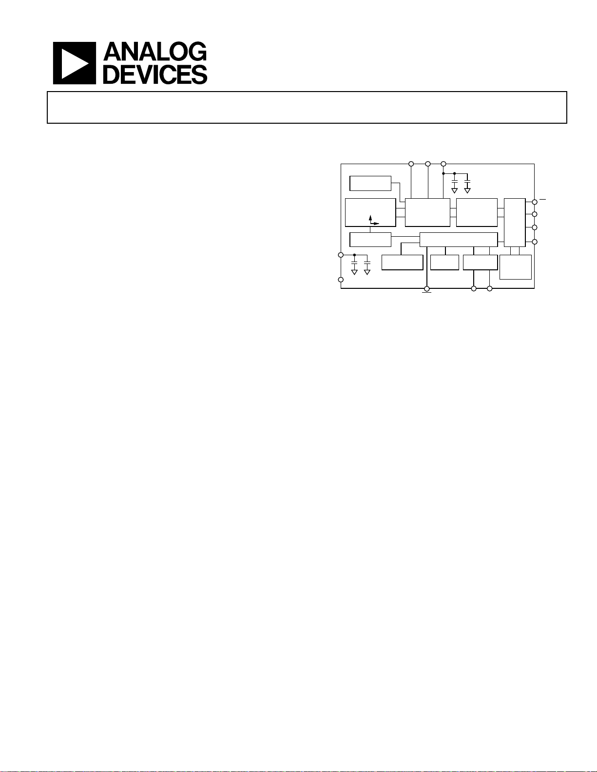
FUNCTIONAL BLOCK DIAGRAM
UX
AUX
ADC
DAC
VREF
DIGITAL
AUXILIARY
I/O
ADIS16204
SPI
PORT
EVENT
CAPTURE
BUFFER
MEMORY
VDD
COM
TEMPERATURE
SENSOR
INERTIAL
MEMS
SENSOR
SELF-TEST
CONDITIONING
CONVERSION
POWER
MANAGEMENT
SIGNAL
ALARMS
PROCESSING
DIGITAL
CONTROL
AND
RST DIO1 DIO2
Figure 1.
CS
SCLK
DIN
DOUT
06448-001
GENERAL DESCRIPTION
The ADIS16204 is a fully-contained programmable impact
sensor in a single compact package enabled by the Analog
Devices, Inc. iSensor™ integration. By enhancing the Analog
Devices iMEMS® sensor technology with an embedded signal
processing solution, the ADIS16204 provides tunable digital
sensor data in a convenient format that can be accessed using
a serial peripheral interface (SPI). The SPI provides access to
measurements for dual-axis linear acceleration, a root sum
square (RSS) of both axes, temperature, power supply, an
auxiliary analog input, and an event capture buffer memory. Easy
access to digital sensor data provides users with a system-ready
device, reducing development time, cost, and program risk.
Unique characteristics of the end system are accommodated
easily through several built-in features, such as a single command
in-system bias null/offset calibration, along with convenient
sample rate control.
Rev. A
Information furnished by Analog Devices is believed to be accurate and reliable. However, no
responsibility is assumed by Analog Devices for its use, nor for any infringements of patents or other
rights of third parties that may result from its use. Specifications subject to change without notice. No
license is granted by implication or otherwise under any patent or patent rights of Analog Devices.
Trademarks and registered trademarks are the property of their respective owners.
The ADIS16204 offers the following embedded features, which
eliminate the need for external circuitry and provide a simplified
system interface:
• Peak sample-and-hold
• Programmable event recording (dual, 1K × 16 bit)
• RSS output (total shock in the XY plane)
• Configurable alarms
• Auxiliary 12-bit ADC and DAC
• Configurable digital I/O port
• Digital self-test function
The ADIS16204 offers two power management features for
managing system-level power dissipation: low power mode
and a configurable shutdown feature.
The ADIS16204 is available in a 9.2 mm × 9.2 mm × 3.9 mm
laminate-based land grid array (LGA) package with a temperature range of −40°C to +105°C.
One Technology Way, P.O. Box 9106, Norwood, MA 02062-9106, U.S.A.
Tel: 781.329.4700 www.analog.com
Fax: 781.461.3113 ©2007 Analog Devices, Inc. All rights reserved.
Page 2

ADIS16204
TABLE OF CONTENTS
Features .............................................................................................. 1
Applications ....................................................................................... 1
Functional Block Diagram .............................................................. 1
General Description ......................................................................... 1
Revision History ............................................................................... 2
Specifications ..................................................................................... 3
Timing Specifications .................................................................. 5
Absolute Maximum Ratings ............................................................ 6
ESD Caution .................................................................................. 6
Pin Configuration and Function Descriptions ............................. 7
Recommended Pad Geometry .................................................... 7
Typical Performance Characteristics ............................................. 8
Theory of Operation ...................................................................... 10
Overview ...................................................................................... 10
Acceleration Sensor .................................................................... 10
Temperature Sensor ................................................................... 10
REVISION HISTORY
10/07—Rev. 0 to Rev. A
Changes to Power Supply Current Specification .......................... 4
Changes to Overview Section ....................................................... 10
6/07—Revision 0: Initial Version
Impact/Shock Response ............................................................ 10
Auxiliary ADC Function ........................................................... 11
Basic Operation .............................................................................. 12
Serial Peripheral Interface ......................................................... 12
Data Output Register Access .................................................... 13
Programming and Control ............................................................ 14
Control Register Overview ....................................................... 14
Control Register Structure ........................................................ 14
Global Commands ..................................................................... 15
Calibration ................................................................................... 15
Operational Control ................................................................... 16
Status and Diagnostics ............................................................... 17
Alarm Detection and Event Capture ....................................... 18
Second-Level Assembly ................................................................. 21
Outline Dimensions ....................................................................... 22
Ordering Guide .......................................................................... 22
Rev. A | Page 2 of 24
Page 3

ADIS16204
SPECIFICATIONS
TA = −40oC to +105°C, VDD = 3.3 V, unless otherwise noted.
Table 1.
Parameter Conditions Axis Min Typ Max Unit
ACCELEROMETER
Output Full-Scale Range X ±70
Y ±37
Sensitivity X 17.125 mg/LSB
Y 8.407 mg/LSB
Nonlinearity 0.2 %
Sensor-to-Sensor Alignment Error 0.1 Degrees
Cross-Axis Sensitivity −5 +5 %
Resonant Frequency 24 kHz
OFFSET
Zero-g Output1 X 0.2
Y 0.2
NOISE
Noise Density 10 Hz − 400 Hz, no postfiltering 1.8 mg/√Hz
FREQUENCY RESPONSE
Sensor Bandwidth (−3 dB) 2-pole Bessel 360 400 440 Hz
Temperature Drift |25°C − T
ACCELEROMETER SELF-TEST STATE2
Output Change When Active At 25°C X 254 LSB
Output Change When Active Y 518 LSB
TEMPERATURE SENSOR
Output at 25°C 1278 LSB
Scale Factor −2.13 LSB/°C
ADC INPUT
Resolution 12 Bits
Integral Nonlinearity (INL) ±2 LSB
Differential Nonlinearity (DNL) ±1 LSB
Offset Error ±4 LSB
Gain Error ±2 LSB
Input Range 0 2.5 V
Input Capacitance During acquisition 20 pF
ON-CHIP VOLTAGE REFERENCE 2.5 V
Accuracy At 25°C −10 +10 mV
Reference Temperature Coefficient ±40 ppm/oC
Output Impedance 70 Ω
DAC OUTPUT 5 kΩ/100 pF to GND
Resolution 12 Bits
Relative Accuracy For Code 101 to Code 4095 4 LSB
Differential Nonlinearity (DNL) 1 LSB
Offset Error ±5 mV
Gain Error ±0.5 %
Output Range 0 to 2.5 V
Output Impedance 2 Ω
Output Settling Time 10 μs
MIN
| or |T
− 25°C| 2 Hz
MAX
g
g
g
g
Rev. A | Page 3 of 24
Page 4

ADIS16204
Parameter Conditions Axis Min Typ Max Unit
LOGIC INPUTS
Input High Voltage, V
Input Low Voltage, V
Logic 1 Input Current, I
Logic 0 Input Current, I
3
2.0 V
INH
0.8 V
INL
VIH = VDD ±0.2 ±1 µA
INH
V
INL
= 0 V −40 −60 A
IL
Input Capacitance, CIN 10 pF
DIGITAL OUTPUTS
Output High Voltage, VOH I
Output Low Voltage, VOL I
= 1.6 mA 2.4 V
SOURCE
= 1.6 mA 0.4 V
SINK
SLEEP TIMER
Timeout Period
4
0.5 128 Seconds
START-UP TIME
Initial 130 ms
Reset recovery 2.5 ms
FLASH MEMORY
Endurance
Data Retention
5
6
20,000 Cycles
TJ = 85°C 20 Years
CONVERSION RATE
Maximum Throughput Rate 4096 SPS
Minimum Throughput Rate 2.066 SPS
POWER SUPPLY
Operating Voltage Range, VDD 3.0 3.3 3.6 V
Power Supply Current
Normal mode, SMPL_PRD ≥ 0x08
12 15 mA
(fS ≤ 910 Hz), at 25°C
Fast mode, SMPL_PRD ≤ 0x07
≥ 1024 Hz), at 25°C
(f
S
37 43 mA
Sleep mode, at 25°C 150 µA
1
Note that gravity can impact this number; zero-g condition assumes both axes oriented normal to the earth’s gravity.
2
Self-test response changes as the square of VDD.
3
Note that the inputs are +5 V tolerant.
4
Guaranteed by design.
5
Endurance is qualified as per JEDEC Standard 22, Method A117 and measured at −40°C, +25°C, +85°C, and +105°C.
6
Retention lifetime equivalent at junction temperature (TJ), 55°C as per JEDEC Standard 22, Method A117. Retention lifetime decreases with junction temperature.
Rev. A | Page 4 of 24
Page 5
SCLK
ADIS16204
TIMING SPECIFICATIONS
TA = +25°C, VCC = +3.3 V, unless otherwise noted.
Table 2.
Parameter Description Min1 Typ Max1 Unit
f
Fast mode2 0.01 2.5 MHz
SCLK
Normal mode2 0.01 1.0 MHz
t
Chip select period, fast mode
DATARATE
Chip select period, normal mode2 100 μs
t
CSHIGH
Chip select high 1/f
tCS Chip select to clock edge 48.8 ns
t
Data output valid after SCLK edge 100 ns
DAV
t
Data input setup time before SCLK rising edge 24.4 ns
DSU
t
Data input hold time after SCLK rising edge 48.8 ns
DHD
tDF Data output fall time 5 12.5 ns
tDR Data output rise time 5 12.5 ns
t
SFS
1
Guaranteed by design; typical specifications are not tested or guaranteed.
2
Based on sample rate selection.
high after SCLK edge
CS
2
40 μs
SCLK
5 ns
t
DATARATE
CS
06448-002
Figure 2. SPI Chip Select Timing
CS
SCLK
DOUT
DIN
t
CS
123456 1516
t
DAV
MSB DB14
t
W/R A5 A4 A3 A2
DB13 DB12 DB10DB11 DB2 LSBDB1
t
DSU
DHD
D2
D1 LSB
t
SFS
06448-003
Figure 3. SPI Timing
(Utilizing SPI Settings Typically Identified as Phase = 1, Polarity = 1)
Rev. A | Page 5 of 24
Page 6

ADIS16204
ABSOLUTE MAXIMUM RATINGS
Table 3.
Parameter Rating
Acceleration (Any Axis, Unpowered, 0.5 ms) 4000 g
Acceleration (Any Axis, Powered, 0.5 ms) 4000 g
VCC to COM −0.3 V to +6.0 V
Digital Input/Output Voltage to COM −0.3 V to +5.5 V
Analog Inputs to COM −0.3 V to +3.5 V
Operating Temperature Range −40°C to +125°C
Storage Temperature Range −65°C to +150°C
Stresses above those listed under Absolute Maximum Ratings
may cause permanent damage to the device. This is a stress
rating only; functional operation of the device at these or any
other conditions above those indicated in the operational
section of this specification is not implied. Exposure to absolute
maximum rating conditions for extended periods may affect
device reliability.
ESD CAUTION
Rev. A | Page 6 of 24
Page 7
PIN CONFIGURATION AND FUNCTION DESCRIPTIONS
ADC
AUX
VDD
13
12
11
10
SCLK
DOUT
DIN
16
1
X
2
3
COM
VREF
15 14
Y
ADIS16204
TOP
VIEW
(Not to Scale)
ADIS16204
AUX DAC
NC
NC
4
CS
56
NC = NO CONNECT
NOTES
1. PINS ARE NOT VISIBLE FROM THE TOP VIEW. THEY ARE
SHOWN FO R CONVENIENCE IN CRE ATING CAD LIBRARY
PARTS.
DIO1
7
8
NC
DIO2
NC
Figure 4. Pin Configuration
Table 4. Pin Function Descriptions
Pin No. Mnemonic Type1Description
1 SCLK I SPI, Serial Clock.
2 DOUT O SPI, Data Out.
3 DIN I SPI, Data In.
4
CS
I SPI, Chip Select, Active Low.
5, 6 DIO1, DIO2 I/O Multifunction Digital Input/Output Pins.
7, 8, 10, 11 NC – No Connect.
9
RST
I Reset, Active Low. This input resets the embedded microcontroller to a known state.
12 AUX DAC O Auxiliary DAC Analog Voltage Output.
13 VDD S +3.3 V Power Supply.
14 AUX ADC I Auxiliary ADC Analog Input Voltage.
15 VREF O Precision Reference Output.
16 COM S Common. Reference point for all circuitry.
1
S = supply; O = output; I = input.
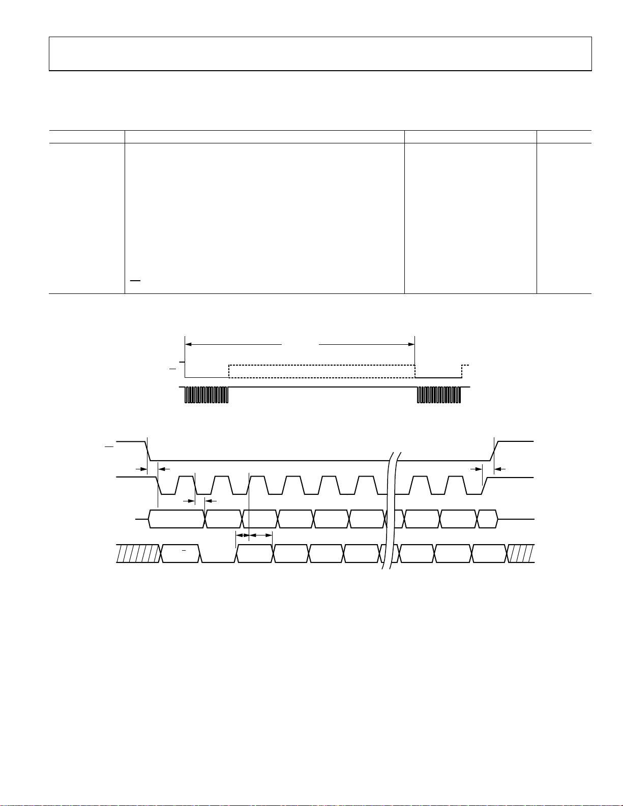
RECOMMENDED PAD GEOMETRY
4.1865
2.6955
8×
8×
9
RST
06448-004
0.670
12×
5.391
8.373
4×
2×
0.500
1.127
16×
9.2mm × 9.2mm S TACKED LGA PACKAGE
16×
06448-005
Figure 5. Example of a Pad Layout
Rev. A | Page 7 of 24
Page 8
ADIS16204
%
TYPICAL PERFORMANCE CHARACTERISTICS
60
50%
40%
30%
20%
% OF POPULATION
10%
0%
0.040 0.125 0.210 0.295
OFFSET BIAS (g)
Figure 6. Bias Offset Distribution, X-Axis
50%
45%
40%
35%
30%
25%
20%
% OF POPULATION
15%
10%
5%
0%
0.045 0.040 0.125 0.2950.210
OFFSET BIAS (g)
Figure 7. Bias Offset Distribution, Y-Axis
0.8
06448-025
026
06448-
0.5
0.4
0.3
0.2
0.1
0
–0.1
Y-AXIS OF FSET BIAS (g)
–0.2
–0.3
–0.4
–40 0 40 80 120
+1 SIGMA
–1 SIGMA
TEMPERATURE ( °C)
Figure 9. Offset Bias Change vs. Temperature, Y-Axis
35
30
25
20
15
% OF POPULATION
10
5
0
0 0.02 0.04 0.06 0.08 0.10 0.12 0.14 0.16
TOTAL OFFSET BIAS CHANGE (g)
0.18
Figure 10. Offset Bias Change, X-Axis vs. Power Supply (3.0 V to 3.6 V)
25
06448-016
06448-019
0.6
0.4
0.2
0
X-AXIS OFFSET BIAS (g)
–0.2
–0.4
–40 0 40 80 120
+1 SIGMA
–1 SIGMA
TEMPERATURE (°C)
Figure 8. Offset Bias Change vs. Temperature, X-Axis
06448-015
20
15
10
% OF POPULATION
5
0
0 0.01 0.02 0.03 0.04 0.05 0.06 0.07
TOTAL OFFSET BIAS CHANGE (g)
0.08
Figure 11. Offset Bias Change, Y-Axis vs. Power Supply (3.0 V to 3.6 V)
8-0200644
Rev. A | Page 8 of 24
Page 9

ADIS16204
30
25
20
15
10
% OF POPULATION
5
0
0.0170 0.0172 0.0174 0.0176 0.0178 0.0180
SENSITIVITY (g/LSB)
06448-027
Figure 12. X-Axis Sensitivity Distribution
40
35
30
25
20
15
SUPPLY CURRENT (mA)
10
5
HIGH PERFO RMANCE M O DE
NORMAL MODE
4.5
4.3
)
g
4.1
3.9
SELF-TEST RESPONSE (
3.7
3.5
–60 –40 –20 0 20 40 60 80 100 120
TEMPERATURE (°C)
Figure 15. Self-Test Response (X and Y Axes) vs. Temperature
200
150
100
50
0
ACCELERATION M AGNITUDE (g)
ACTUAL ACCELERAT ION PROFI LE
X_ACCL
Y_ACCL
6448-022
0
2.8 2.9 3.0 3.1 3.2 3.3 3.4 3.5 3.6 3.7 3.8
SUPPLY VOLT AG E ( V)
Figure 13. Supply Current vs. Supply Voltage
400
300
200
SLEEP CURRENT ( µ A)
100
0
–50 –35 –20 –5 10 25 40 55 70 85 100
+1 SIGMA
–1 SIGMA
TEMPERATURE (°C)
06448-023
06448-032
–50
0 20406080100120
SAMPLE
Figure 16. Overrange Recovery, Sample Rate = 4096 SPS
6448-029
Figure 14. Sleep Current vs. Temperature
Rev. A | Page 9 of 2
4
Page 10

ADIS16204
A
(
THEORY OF OPERATION
OVERVIEW
The ADIS16204 integrates a dual-axis ±70 g/±37 g MEMS
acceleration sensor into a complete impact/shock measurement
and recording system. The integrated mixed signal processing
circuit digitizes the sensor data, applies corrections factors,
provides many user-programmable features, and offers a simple
communication conduit: the serial peripheral interface (SPI).
ACCELERATION SENSOR
The ADIS16204 base sensor core provides a fully differential
sensor structure and circuit path, resulting in substantial
rejection of electromagnetic interference (EMI) effects. It
uses electrical feedback with zero-force feedback for improved
accuracy and stability. The sensor’s resonant frequency is well
beyond the cut-off frequency of the filter, which adds further
noise rejection to the sensor signal conditioning circuit.
ANCHOR
MOVABLE
PLATE
CAPACITORS
UNIT
SENSING
TION
ACCELER
CELL
MOVING
PLATE
FIXED
PLATES
ANCHOR
Figure 17. Simplified View of a Sensor Under Acceleration
Figure 17 is a simplified view of one of the differential sensor
elements. Each sensor includes several differential capacitor
unit cells. Each cell is composed of fixed plates attached to the
substrate and movable plates attached to the frame. Displacement of the frame changes the differential capacitance, which
is measured by the on-chip circuitry.
Complementary 200 kHz square waves drive the fixed plates.
Electrical feedback adjusts the amplitudes of the square waves
such that the ac signal on the moving plates is 0 V. The feedback
signal is linearly proportional to the applied acceleration. This
unique feedback technique ensures that there is no net electrostatic force applied to the sensor. The differential feedback control
signal is also applied to the input of the filter, where it is filtered
and converted to a single-ended signal.
FRAME
UNIT
FORCING
CELL
06
6448-0
IMPACT/SHOCK RESPONSE
The sensor’s mechanical structure provides a linear measurement range that is 8 times that of each axis’ actual output
measurement range. Therefore, when considering the response
to high-g, short duration events, the 2-pole, 400 Hz, low-pass
Bessel filter network influences the output response. Figure 18
provides a frequency response for this signal chain. In Figure 19,
the X-axis accelerometer experiences a 560 g shock event that
lasts 0.1 ms, causing the output response to reach 70 g. For users
that need to avoid output saturation, keeping the integration of
the event’s acceleration response (acceleration-time product in
the case of Figure 19) below 56 g-ms is critical.
10
X: 418.9
0
–10
–20
MAGNITUDE (dB)
–30
–40
–50
10 100 1k 10k
FREQUENCY (Hz)
Figure 18. ADIS16204 Frequency Response
600
550
500
450
)
g
400
350
300
250
200
IMPACT MAGNITUDE
150
100
50
0
–0.50 –0.25 0.25 0.50 0.75 1.00 1.25 1.50 1.75 2.000
560g, 0.1ms, SIMULATE D SHOCK
Figure 19. ADIS16204 Shock Response
Y: –3.291
70g, FILTERED RESPONSE
TIME (ms)
06448-007
06448-008
TEMPERATURE SENSOR
This sensor reflects the sensor’s junction temperature and
provides a convenient temperature measurement for systemlevel characterization and calibration feedback.
Rev. A | Page 10 of 24
Page 11

V
ADIS16204
AUXILIARY ADC FUNCTION
The auxiliary ADC function integrates a standard 12-bit ADC
into the ADIS16204 to digitize other system-level analog signals. The output of the ADC can be monitored through the
AUX_ADC control register, as defined in Ta b le 6 . The ADC is
a 12-bit successive approximation converter. The output data
is presented in straight binary format with the full-scale range
extending from 0 V to V
calibrated 2.5 V reference is also provided.
Figure 20 shows the equivalent circuit of the analog input structure of the ADC. The input capacitor (C1) is typically 4 pF and
can be attributed to parasitic package capacitance. The two diodes
provide ESD protection for the analog input. Care must be
taken to ensure that the analog input signals never exceed the
supply rails by more than 300 mV. This causes the diodes to
become forward-biased and to start conducting. The diodes
can handle 10 mA without causing irreversible damage. The
resistor is a lumped component that represents the on resistance
of the switches. The value of this resistance is typically 100 Ω.
Capacitor C2 represents the ADC sampling capacitor and is
typically 16 pF.
. A high precision, low drift, factory
REF
DD
D
C1
Figure 20. Equivalent Analog Input Circuit
Conversion Phase: Switch Open
D
Track Phase: Switch Closed
C2
R1
06448-010
For ac applications, removing high frequency components from
the analog input signal is recommended by the use of a low-pass
filter on the analog input pin.
In applications where harmonic distortion and signal-to-noise
ratio are critical, the analog input must be driven from a low
impedance source. Large source impedances significantly affect
the ac performance of the ADC. This can necessitate the use of
an input buffer amplifier. When no input amplifier is used to drive
the analog input, the source impedance should be limited to
values lower than 1 kΩ.
Rev. A | Page 11 of 24
Page 12

ADIS16204
K
BASIC OPERATION
The ADIS16204 is designed for simple integration into industrial
system designs, requiring only a power supply and a 4-wire,
industry-standard SPI. The SPI provides access to the ADIS16204’s
register structure, which controls access to all sensor output data
and controls for the device’s programmable features. Each register
is 16 bits in length and has its own unique bit map. The 16 bits
in each register consist of an upper byte (Bit 8 to Bit 15) and a
lower byte (Bit 0 to Bit 7), each of which has its own 6-bit address.
SERIAL PERIPHERAL INTERFACE
The ADIS16204 SPI port includes four signals: chip select
CS
), serial clock (SCLK), data input (DIN), and data output
(
(DOUT). The
frames each SPI event. When this signal is high, the DOUT
lines are in a high impedance state and the signals on DIN
and SCLK have no impact on operation. A complete data frame
contains 16 clock cycles. Because the SPI port operates in full
duplex mode, it supports simultaneous, 16-bit receive (DIN)
and transmit (DOUT) functions during the same data frame.
See Table 2, Figure 2, and Figure 3 for detailed timing and
operation of the SPI port.
CS
line enables the ADIS16204 SPI port and
CS
DATA FRAME
Writing to Registers
Figure 21 displays a typical data frame for writing a command
to a control register. In this case, the first bit of the DIN sequence is
a 1, followed by a 0, the 6-bit address, and the 8-bit data command.
Because each write command covers a single byte of data, two
data frames are required when writing to the entire 16-bit space of
a register. The DIN bits clock into the ADIS16204 on the rising
edge of SCLK.
Reading from Registers
Reading the contents of a register requires a modification to
the sequence in the DIN sequence shown in Figure 21. As
shown in Figure 22, the first two bits in the DIN sequence are 0,
followed by 6 address bits. Each register has two addresses (upper,
lower), but either one can be used to access its entire 16 bits of
data. The final 8 bits of the DIN sequence are irrelevant and can be
counted as don’t cares during a read command. During the next
data frame, the DOUT sequence contains the register’s 16-bit
data. The ADIS16204 clocks out the first DOUT bit on the falling
edge of the
CS
line and clocks out the rest of the DOUT bits on the
falling edges of the SCLK signal. Although a single read command
requires two separate data frames, the full duplex mode minimizes this overhead, requiring only one extra data frame when
continuously sampling.
SCL
DIN
W/R A5 A4 A3 A2 A1 A0 DC7 DC6 DC5 DC4 DC3 DC2 DC1 DC0
WRITE = 1
READ = 0
REGISTE R ADDRES S DATA FOR WRI TE COMMANDS
Figure 21. DIN Bit Sequence
DON’T CARE FOR READ COMMANDS
06448-011
CS
SCLK
DIN
W/R BIT
DOUT
DATA FRAME
ADDRESS DON’ T CARE NEXT COMMAND
ZERO
BASED ON PREVIOUS COMMAND
Figure 22. SPI Sequence for Read Commands
DATA FRAME
16-BIT REG ISTER CONTENTS
06448-012
Rev. A | Page 12 of 24
Page 13

DATA OUTPUT REGISTER ACCESS
Table 6 provides an overview of each data output register,
along with their function, address, and relevant decoding
information.
Sensor Output Data
The ADIS16204 provides access to X- and Y-axis acceleration
measurements, combined accelerations measurements (root
sum square of X and Y), peak acceleration, power supply measurements, temperature measurements, an auxiliary 12-bit
ADC channel, and the event-capture buffer memory.
Peak Sample-and-Hold Output Registers
The ADIS16204 monitors the X, Y and XY acceleration
measurements and holds the maximum value and polarity
for each parameter. The X_PEAK_OUT, Y_PEAK_OUT, and
XY_PEAK_OUT registers provide access to these maximum
values. See the COMMAND register for how to clear these
registers.
Register Access
This output data is continuously updating internally, regardless
of user read rates. The bit map in Table 5 describes the structure of
ADIS16204
all output data registers in the ADIS16204. The upper byte is
always first in register read sequences.
Table 5. Output Bit Assignments
MSB LSB
ND EA D13 D12 D11 D10 D9 D8
D7 D6 D5 D4 D3 D2 D1 D0
The MSB holds the new data (ND) indicator. When the output
registers are updated with new data, the ND bit goes to a 1 state.
After the output data is read, it returns to a 0 state. The error/
alarm bit (EA) is used to indicate a system error or an alarm
condition that can result from a number of conditions, such as
a power supply that is out of the specified operating range (see
the Status and Diagnostics section for more details). The output
data is either 12 bits or 14 bits in length. For all of the 12-bit
output data, Bit D13 and Bit D12 are assigned don’t care status.
The output data register map located in Table 6 provides all of
the necessary details for accessing each register’s data. Figure 23
provides an example of the SPI sequence.
Table 6. Data Output Register Information
Scale Factor
Name Function Register Resolution (Bits) Data Format
(per LSB)
SUPPLY_OUT Power supply 0x03, 0x02 12 Binary 1.22 mV
XACCL_OUT X-axis acceleration 0x05, 0x04 14 Twos complement 17.125 mg
YACCL_OUT Y-axis acceleration 0x07, 0x06 14 Twos complement 8.407 mg
AUX_ADC Auxiliary analog input data 0x09, 0x08 12 Binary 0.61 mV
TEMP_OUT1 Sensor temperature data 0x0B, 0x0A 12 Binary −0.47°C
X_PEAK_OUT2 Peak, X-axis acceleration 0x0D, 0x0C 14 Twos complement 17.125 mg
Y_PEAK_OUT2 Peak, Y-axis acceleration 0x0F, 0x0E 14 Twos complement 8.407 mg
XY_RSS_OUT3 XY combined acceleration (RSS) 0x19, 0x18 14 Binary 17.125 mg
XY_PEAK_OUT
CAPT_BUF_14 Capture Buffer 1 Output Register 0x1D, 0x1C
CAPT_BUF_24 Capture Buffer 2 Output Register 0x1F, 0x1E
1
25°C, nominal output is equal to 1278 LSB.
2
The peak levels in these registers accumulate, storing the greatest value measured (polarity is captured—except for XY_PEAK_OUT), until they are cleared using the
COMMAND register.
3
This is a measure of the total shock absorbed by the package in the XY plane, and is the result of a root sum square of X and Y acceleration measurements.
4
See the Alarm Detection and Event Capture section for more details.
2, 3
Peak, XY combined output (RSS) 0x1B, 0x1A 14 Binary 17.125 mg
See the Alarm Detection and Event Capture section, Table 37,
and Table 38
CS
SCLK
DIN
W/R BIT = 0
ADDRESS = 000101
DOUT
DATA = 1011 1101 1101 1110
NEW DATA, NO ALARM, XACCL_O UT = –10.377 g
Figure 23. Example of an Output Timing/Coding Diagram
Rev. A | Page 13 of 24
06448-013
Page 14

ADIS16204
PROGRAMMING AND CONTROL
CONTROL REGISTER OVERVIEW
The ADIS16204 offers many programmable features controlled
by writing commands to the appropriate control registers. The
following features are available for configuration:
• Global commands
• Calibration
• Operational control
• Sample rate
• Power management
• DAC output
• Digital I/O
• Operational status and diagnostics
• Self-test
• Status conditions
• Alarms
CONTROL REGISTER STRUCTURE
The ADIS16204 uses a temporary, SRAM-based memory structure to facilitate the control registers displayed in Tabl e 7. The
start-up configuration is stored in a flash memory structure that
automatically loads into the control registers during the start-up
sequence. Each nonvolatile register has a corresponding flash
memory location for storing the latest configuration contents.
Because flash memory has endurance limitations, the contents
of each nonvolatile register must be stored to flash manually.
Note that the contents of the control register are only nonvolatile when they are stored to flash. The flash update command,
made available in the COMMAND register, provides this function.
The ENDURANCE register provides a counter, which allows
for memory reliability management against the flash memory’s
write cycle specification.
• Event capture
Table 7. Control Register Mapping
Name Type Volatility
ENDURANCE R Nonvolatile 0x01, 0x00 2 Flash memory write counter Table 26
0x02 to 0x0F 14 Output data registers Table 6
XACCL_NULL R/W Nonvolatile 0x11, 0x10 2 X-axis offset null calibration register Table 10
YACCL_NULL R/W Nonvolatile 0x13, 0x12 2 Y-axis offset null calibration register Table 11
XACCL_SCALE R/W Nonvolatile 0x15, 0x14 2 X-axis scale factor calibration register Table 12
YACCL_SCALE R/W Nonvolatile 0x17, 0x16 2 Y-axis scale factor calibration register Table 13
0x18 to to 0x1B 4 Output data registers Table 6
CAP_BUF_1 R Volatile 0x1D, 0x1C 2 Capture buffer output register 1 Table 37, Ta ble 38
CAP_BUF_2 R Volatile 0x1F, 0x1E 2 Capture buffer output register 2 Table 37, Table 38
ALM_MAG1 R/W Nonvolatile 0x21, 0x20 2 Alarm 1 amplitude threshold Table 32, Ta ble 34
ALM_MAG2 R/W Nonvolatile 0x23, 0x22 2 Alarm 2 amplitude threshold Table 33, Ta ble 34
0x24 to 0x27 2 Reserved
ALM_CTRL R/W Nonvolatile 0x29, 0x28 2 Alarm source control register Table 30, Ta ble 31
CAPT_PNTR R/W Volatile 0x2B, 0x2A 2 Capture register address pointer Table 39, Tab le 40
0x2A to 0x2F 6 Reserved
AUX_DAC R/W Volatile 0x31, 0x30 2 Auxiliary DAC data Table 19, Table 20
GPIO_CTRL R/W Volatile 0x33, 0x32 2 Auxiliary digital I/O control register Table 21, Table 22
MSC_CTRL R/W Nonvolatile20x35, 0x34 2 Miscellaneous control register Table 24, Table 25
SMPL_PRD R/W Nonvolatile 0x37, 0x36 2 ADC sample period control register Table 15, Table 16
CAPT_CFG R/W Nonvolatile 0x39, 0x38 2 Capture configuration register Table 35, Table 36
SLP_CNT W Volatile 0x3B, 0x3A 2
STATUS R Volatile 0x3D, 0x3C 2 System status register Table 27, Table 28
COMMAND W N/A 0x3F, 0x3E 2 System command register Table 8, Table 9
1
In order to establish nonvolatile status, the flash memory must be updated after updating the control registers.
2
Bit 8 clears after the internal self-test sequence completes, effectively making this bit volatile.
1
Address Bytes Function Reference Table
Counter used to determine length of
power-down mode
Table 17, Ta ble 18
Rev. A | Page 14 of 24
Page 15

GLOBAL COMMANDS
The ADIS16204 provides global commands, which simplify
many common operations. The COMMAND register provides
command bits for each function. Writing a 1 to the assigned
command bit exercises its function. The flash update copies the
contents of all nonvolatile registers into their assigned, nonvolatile,
flash memory locations. This process takes approximately 50 ms
and requires a power supply that is within the specified operating
range. After waiting the appropriate time for the flash update to
complete, verify successful completion by reading the STATUS
register (flash update error = zero, if successful). If the flash
update was not successful, reading this error bit accomplishes
two things: (1) alert system processor to try again, and (2) clear
the error flag, which is required for flash memory access.
The software reset command restarts the internal processor,
which loads all registers with the contents in their flash memory
locations. The DAC data latch command loads the contents of
AUX_DAC into the DAC latches. Because the AUX_DAC
contents must be updated one byte at a time, this command
ensures a stable DAC output voltage during updates.
Calibration Commands
The autonull command provides a simple method for removing
offset from the sensor outputs. This command takes separate
64-sample measurements for each axis (X, Y), then loads the
opposite value into each axis’ offset null register. The accuracy
of this operation depends on zero force or motion during the
64-sample timeframe. The factory calibration restore sets the
scale and offset null registers (XACCL_NULL, for example)
back to their default values. For more information on
ADIS16204 calibration, see the Calibration section.
Event Capture Commands
The COMMAND register provides four different functions that
simplify the process of using the event capture function. The
reset-capture pointer function sets the contents of the capture
pointer to its initial value of 0x0001. The clear capture flash,
clear capture buffer, and capture flash copy commands are selfdescriptive. The capture flash copy takes approximately 120 ms
to complete and serves the purpose of copying the capture buffer
into nonvolatile flash memory. See the Alarm Detection and
Event Capture section for more information.
ADIS16204
Table 9. COMMAND Bit Descriptions
Bit Description
15:11 Not used
10 Reset-capture pointer (set CAPT_PNTR to 0x0001)
9 Clear capture flash (nonvolatile back-up)
8 Clear capture buffer (SRAM)
7 Software reset
6 Copy capture buffer to nonvolatile flash
5 Clear peak output registers, (reset them to 0x0000)
4 Clear status register (reset all bits to 0)
3 Flash update—saves nonvolatile register settings
2 DAC data latch
1 Factory calibration restore
0 Autonull
CALIBRATION
In addition to the factory calibration, the ADIS16204 provides
a user configurable calibration for systems that require accuracy
improvements. For example, a vehicle system may require better
resolution to separate a minor bump from a hard brake event.
In cases like this, the ADIS16204 provides configuration registers
that adjust both offset and sensitivity (gain) on both X- and
Y-axes. The following relationship describes the calibration
function:
y = mx + b
where:
y is the calibrated output data.
m is the scale factor multiplier [XACCL_SCALE/YACCL_SCALE].
x is the precalibration data.
b is the offset adder [XACCL_NULL/YACCL_NULL].
Assuming zero offset and nominal scale factor (sensitivity),
the offset adjustment range for the X-axis is ±35.054 g and
±17.527 g for the Y-axis. Assuming zero offset, the scale factor
adjustment range is 0 to 2.
Table 10. XACCL_NULL Register Definition
Address Scale1 Default Format Access
0x11, 0x10 17.125 mg 0x0000
1
Scale is the weight of each LSB.
Twos
complement
R/W
Table 8. COMMAND Register Definition
Address Default Format Access
0x3F, 0x3E N/A N/A W only
Rev. A | Page 15 of 24
Table 11. YACCL_NULL Register Definition
Address Scale1 Default Format Access
0x13, 0x12 8.407 mg 0x0000
1
Scale is the weight of each LSB.
Twos
complement
R/W
Table 12. XACCL_SCALE Register Definition
Address Scale1 Default2 Format Access
0x15, 0x14 0.0488% 0x0800 Binary R/W
1
Scale is the weight of each LSB.
2
Equates to a scale factor of one.
Page 16

ADIS16204
Table 13. YACCL_SCALE Register Definition
Address Scale1 Default2 Format Access
0x17, 0x16 0.0488% 0x0800 Binary R/W
1
Scale is the weight of each LSB.
2
Equates to a scale factor of one.
Table 14. Calibration Register Bit Descriptions
Bit Description
15:12 Not used
11:0 Data bits
OPERATIONAL CONTROL
Internal Sample Rate
The internal sample rate defines how often data output variables
are updated, independent of the rate at which they are read out
on the SPI port. The SMPL_PRD register controls the ADIS16204
internal sample rate and has two parts: a selectable time base and
a multiplier. The following relationship produces the sample rate:
T
= TB × (NS + 1)
S
where:
T
is the sample period.
S
is the time base.
T
B
N
is the increment setting.
S
The default value is the maximum 4096 SPS, and the contents of
this register are nonvolatile.
Table 15. SMPL_PRD Register Definition
Address Default Format Access
0x37, 0x36 0x0001 N/A R/W
Table 16. SMPL_PRD Bit Descriptions
Bit Description
15:8 Not used
7 Time base
0 = 122.07 μs, 1 = 3.784 ms
6:0 Multiplier
Here is an example calculation of the sample period for the
ADIS16204:
If SMPL_PRD = 0x0007, B7 − B0 = 00000111
B7 = 0 → T
B6…B0 = 000000111 → N
T
= TB × (NS + 1) = 122.07 μs × (7 + 1) = 976.56 μs
S
f
= 1∕TS = 1024 SPS
S
The sample rate setting has a direct impact on the SPI data
rate capability. For sample rates ≥1024 SPS, the SPI SCLK can
run at a rate up to 2.5 MHz. For sample rates <1024 SPS, the SPI
SCLK can run at a rate up to 1 MHz.
= 122.07 μs
B
= 7
S
The sample rate setting also affects the power dissipation.
When the sample rate is set below 1024 SPS, the power
dissipation typically reduces by a factor of 68%. The two
different modes of operation offer a system-level trade-off
between performance (sample rate, serial transfer rate) and
power dissipation.
Power Management
In addition to offering two different performance modes for
power optimization, the ADIS16204 offers a programmable
shutdown period. Writing the appropriate sleep time to the
SLP_CNT register shuts the device down for the specified
time. The following example provides an illustration of this
relationship:
B7 … B0 = 00000110
Sleep period = 3 seconds
After completing the sleep period, the ADIS16204 returns to
normal operation.
Table 17. SLP_CNT Register Definition
Address Scale1 Default Format Access
0x3B, 0x3A 0.5 sec 0x0000 Binary W only
1
Scale is the weight of each LSB.
Table 18. SLP_CNT Bit Descriptions
Bit Description
15:8 Not used
7:0 Data bits
Auxiliary DAC
The auxiliary DAC provides a 12-bit level adjustment function.
The AUX_DAC register controls the operation of this feature.
It offers a rail-to-rail buffered output that has a range of 0 V to
2.5 V. The DAC can drive its output to within 5 mV of the
ground reference when it is not sinking current. As the output
approaches ground, the linearity begins to degrade (100 LSB
beginning point). As the sink current increases, the nonlinear
range increases. The DAC output latch function, contained in
the COMMAND register, provides continuous operation while
writing to each byte of this register. The contents of this register
are volatile, which means that the desired output level must be
set after every reset and power cycle event.
Table 19. AUX_DAC Register Definition
Address Scale
1
Default Format Access
0x31, 0x30 0.6105 mV 0x0000 Binary R/W
1
Scale is the weight of each LSB. In this case, it represents 4095 codes over
the 2.5 V range out of output voltage.
Table 20. AUX_DAC Bit Descriptions
Bit Description
15:12 Not used
11:0 Data bits
Rev. A | Page 16 of 24
Page 17

General-Purpose I/O
The ADIS16204 provides two general-purpose pins that
enable digital I/O control using the SPI. The GPIO_CTRL
control register establishes the configuration of these pins
and handles the SPI-to-pin controls. Each pin provides the
flexibility of both input (read) and output (write) operations.
For example, writing a 0x0202 to this register establishes Line 1
as an input and Line 2 as an output that is in a 1 state. Writing
0x0000 to this register establishes both lines as inputs. When
one (or both) of these lines is configured as an input, reading
the assigned bit (Bit 8 and/or Bit 9) provides access to the input
on this input pin.
The digital I/O lines are also available for data-ready and alarm/
error indications. In the event of conflict, the following priority
structure governs the digital I/O configuration:
1. GPIO_CTRL
2. MSC_CTRL
3. ALM_CTRL
Table 21. GPIO_CTRL Register Definition
Address Default Format Access
0x33, 0x32 0x0000 N/A R/W
Table 22. GPIO_CTRL Bit Descriptions
Bit Description
15:10 Not used
9 General-purpose I/O Line 2 polarity
1 = high, 0 = low
8 General-purpose I/O Line 1 polarity
1 = high, 0 = low
7:2 Not used
1 General-purpose I/O Line 2, data direction control
1 = output, 0 = input
0 General-purpose I/O Line 1, data direction control
1 = output, 0 = input
STATUS AND DIAGNOSTICS
The ADIS16204 provides a number of status and diagnostic
functions. Tabl e 23 provides a summary of these functions,
along with their appropriate control registers.
Table 23. Status and Diagnostic Functions
Function Register
Data-ready I/O indicator MSC_CTRL
Self-test, mechanical check for MEMS sensor MSC_CTRL
Software check for error conditions STATUS
Flash memory endurance ENDURANCE
Data-Ready I/O Indicator
The data-ready function provides an indication of new output
data. The MSC_CTRL register provides the opportunity to
configure either of the general-purpose I/O pins (DIO1 and DIO2)
as a data-ready indicator signal. When configured as a data ready
indicator, the duty cycle is 20% (±10% tolerance).
Self-Test
The MSC_CTRL register also provides a self-test function
that verifies the mechanical integrity of the MEMS sensor. A
self-test exercises the mechanical structure and signal conditioning circuit: from sensor element to data out. The internal
test provides a simple, two-step process for checking the MEMS
sensor: (1) start the process by writing a 1 to Bit 8 in the
MSC_CTRL register, (2) wait 35 ms, and (3) check the result
by reading Bit 5 of the STATUS register.
The device is configured to perform a self-test at power on.
Writing a 1 to Bit 10 of the MSC_CTRL register disables this
function for future start-up sequences, reducing the start-up
time. For reference, the result of the electrostatic deflection
of each axis is available by reading the XACCL_OUT and/or
YACCL_OUT registers. As an additional indicator of self-test,
the new data bit is not active while in this mode.
Table 24. MSC_CTRL Register Definition
Address Default Format Access
0x35, 0x34 0x0000 N/A R/W
Table 25. MSC_CTRL Bit Descriptions
Bit Description
15:12 Not used
11 Store capture to flash after capture buffer fills up
1 = enabled, 0 = disabled
10 Self-test at power-on
1 = disabled, 0 = enabled
9 Not used
8 Self-test enable (temporary, bit is volatile)
1 = enabled, 0 = disabled
7:3 Not used
2 Data-ready enable
1 = enabled, 0 = disabled
1 Data-ready polarity
1 = active high, 0 = active low
0 Data-ready line select
1 = DIO2, 0 = DIO1
Flash Memory Endurance
The ENDURANCE register maintains a running count of writes to
the flash memory. This provides a convenient tool for managing
the reliability of the on-chip memory. Once it reaches its maximum value of 32,767, it wraps around to zero and starts over.
Table 26. ENDURANCE Register Definition
Address Default Format Access
0x01, 0x00 N/A Binary R only
ADIS16204
Rev. A | Page 17 of 24
Page 18

ADIS16204
STATUS Conditions
The STATUS register contains the following error-condition
flags: alarm conditions, self-test status, SPI communication
failure, capture buffer full, control register update failure, and
power supply out of range. See Tabl e 27 and Ta bl e 28 for the
appropriate register access and bit assignment for each flag.
The bits assigned for checking power supply range automatically reset to zero when the error condition no longer exists.
Clearing the remaining error-flag bits requires a single write
command to the COMMAND register (write a 1 to Bit 4).
See Tab le 8 and Ta bl e 9 for the configuration details of the
COMMAND register. If the error condition still exists after
exercising the COMMAND register to clear the bits, the appropriate error flag bit returns to 1 during the next sampling cycle.
All bits in the STATUS register are volatile.
Table 27. STATUS Register Definition
Address Default Format Access
0x3D, 0x3C 0x0000 N/A R only
Table 28. STATUS Bit Descriptions
Bit Description
15:13 Not used
12 Capture buffers full
11:10 Not used
9 Alarm 2 status
1 = active, 0 = inactive
8 Alarm 1 status
1 = active, 0 = inactive
7:6 Not used
5 Self-test diagnostic error flag
1 = error condition, 0 = normal operation
4 Not used
3 SPI communications failure
1 = error condition, 0 = normal operation
2 Flash update failed
1 = error condition, 0 = normal operation
1 Power supply above 3.625 V
1 = > 3.625 V, 0 = < 2.975 V (normal)
0 Power supply below 2.975 V
1 = < 2.975 V, 0 = > 2.975 V (normal)
ALARM DETECTION AND EVENT CAPTURE
The ADIS16204 provides alarm detection and event capture
functions, which monitor critical internal and external
operating conditions. Six factory standard alarms monitor
the AIDS16204 for normal operation. Two programmable
alarms provide monitoring for system-critical conditions,
which reduces the external processing burden for this function.
Alarm monitoring includes both software (STATUS register)
and hardware options (DIO1 and DIO2 configuration,
ALM_CTRL register). In addition, the programmable alarms
can trigger an event capture function, which provides time
recording, much like a single event capture function on a digital
oscilloscope. Table 29 provides a summary of the functions
available for configuring the alarms.
Alarm Configuration
1. Program the Output Data to Monitor.
Essentially, this establishes the trigger source, by configuring
the upper byte of the ALM_CTRL register. See Tabl e 31 for the
proper bit assignments. For example, the following pseudo code
establishes X acceleration as the trigger for Alarm 2 and Y acceleration as the trigger for Alarm 1:
• Write 0x23 to Address 0x29 [ALM_CTRL].
2. Program the Trigger Levels and Polarity.
This requires two write commands for each alarm, to the
ALM_MAG1 and ALM_MAG2 registers. For example, use
the following pseudo code to establish greater than 7.4 g as
the trigger threshold for both channels:
• Write 0x81 to Address 0x21 [ALM_MAG1].
• Write 0xB0 to Address 0x20 [ALM_MAG1].
• Write 0x83 to Address 0x23 [ALM_MAG2].
• Write 0x70 to Address 0x22 [ALM_MAG2].
The ALM_MAG1 and ALM_MAG2 values are calculated by:
X = 7.4 g = 432 codes = 00 0001 1011 0000 (Bit 0 to Bit 13)
Y = 7.4 g = 880 codes = 00 0011 0111 0000 (Bit 0 to Bit 13)
Bit 15 in both registers must be set to 1 in order to denote
greater than polarity.
3. Set Up a Digital I/O Line as an Alarm Indicator.
This step requires configuration of the lower byte in the
ALM_CTRL. If software monitoring, using the STATUS
register, is the preferred alarm-checking method, then this
step is not required. The following pseudocode establishes
Digital I/O Line 2 as a positive signal, alarm indicator:
• Write 0x07 to Address 0x28 [ALM_CTRL].
See Tab le 3 1 for the configuration options available for this
function. As noted earlier, the digital I/O lines are shared, so
use of them as an alarm indicator requires that it not be in use
as a data-ready or general-purpose I/O pin.
Rev. A | Page 18 of 24
Page 19

Table 29. Alarm and Event Capture Configuration Registers
Register Parameter/Function Default Setting
ALM_CTRL Alarm trigger source None
ALM_CTRL Capture buffer triggers Disabled
ALM_CTRL Digital alarm output Disabled
ALM_MAG1/
ALM_MAG 2
ALM_MAG1/
ALM_MAG 2
CAPT_CFG Capture data sources
CAPT_CFG Capture buffer size 1024 samples
CAPT_CFG Pretrigger data size 128 samples
COMMAND Reset capture pointer N/A
COMMAND Clear capture buffer N/A
COMMAND Clear capture flash N/A
COMMAND Clear buffer full flag N/A
COMMAND
MSC_CTRL
SMPL_PRD Sample rate 4096 SPS
Table 30. ALM_CTRL Register Definition
Address Default Format Access
0x29, 0x28 0x0000 N/A R/W
Table 31. ALM_CTRL Bit Descriptions
Bit Value Description
15:12 Trigger source selection, Alarm 2
0000 Disable
0001 Power supply
0010 X-acceleration
0011 Y-acceleration
0100 Auxiliary ADC
0101 Temperature sensor
1000 XY RSS acceleration
11:8 Trigger source selection, Alarm 1 (See Alarm2)
7 Not used
6 Capture trigger activation, Alarm 2
5 Not used
4 Capture trigger activation, Alarm 1
3 Not used
2 Alarm indicator, using DIO1/2
1 Alarm indicator polarity
0 Alarm indicator line selection
Alarm trigger levels 0
Alarm trigger directions Less than
1: X acceleration
2: Y acceleration
Save captured data to
N/A
nonvolatile flash
Autosave captured
Disabled
data to nonvolatile flash
1 = enabled, 0 = disabled
1 = enabled, 0 = disabled
1 = enabled, 0 = disabled
1 = active high, 0 = active low
1 = DIO2, 0 = DIO1
ADIS16204
Table 33. ALM_MAG2 Register Definition
Address Default Format Access
0x23, 0x22 0x0000 N/A R/W
Table 34. ALM_MAG1/ALM_MAG 2 Bit Designations
Bit Description
15 Comparison polarity
1 = greater than, 0 = less than
14 Not used
13:0
Event Capture Overview
The ADIS16204 also provides a dual-channel, capture function.
Figure 24 provides an example of a captured waveform. A dedicated set of programmable control registers govern the operation
of this function, controlling the data source: trigger settings
(level, direction, and data source), memory depth, pretrigger
data length, and data storage. In systems that require specific
event monitoring, this feature simplifies system integration by
reducing the burden on the system’s processor. One convenient
feature is the fact that the trigger source does not have to be the
data that is captured.
Event Capture Configuration
The event capture buffers use the alarms as their trigger source.
Therefore, the first two configuration steps are the same. After
setting the trigger data source(s) and threshold(s), follow Step 1
through Step 5 to complete the event capture setup.
1. Program the Data Source to Capture.
This requires a single write cycle, to configure the upper byte of
the CAPT_CFG register. For example, use the following pseudo
code to set X acceleration and Y acceleration as the data sources
for Capture Buffer 2 and Capture Buffer 1 respectively:
Data bits: format matches source data format
(see Table 5 and Table 6)
20
15
10
5
0
–5
–10
PRE-TRIGGER
Y-AXIS IMPACT MAGNITUDE (g)
DATA
LENGTH
–15
–20
0 100 200 300 400 500 600 700 800 900 1000
DATA SOURCE: Y-AX IS ACCELERATI ON
TRIGGER THRESHOL D: 7.4g
SAMPLE –
Figure 24. Event Capture Example
f
= 4096SPS
s
• Write 0x23 to Address 0x39 [CAPT_CFG].
06448-014
Table 32. ALM_MAG1 Register Definition
Address Default Format Access
0x21, 0x20 0x0000 N/A R/W
Rev. A | Page 19 of 24
Page 20

ADIS16204
2. Configure the Capture Backup Memory.
Setting Bit 11 of the MSC_CTRL register to a 1 enables the
event capture back-up function, effectively making it nonvolatile.
When enabled, this function copies the contents of the capture
buffer (right after it fills) to flash memory and restores it upon
reset or powering the device on. It continues to do so until the
buffer is cleared, using the COMMAND register. To enable this
feature, use the following pseudo code:
• Write 0x08 to Address 0x35 [MSC_CTRL].
3. Clear the Capture Memory Locations.
Use the following pseudo code to clear both the normal capture
locations (SRAM) and their respective flash memory locations:
• Write 0x03 to Address 0x3F [COMMAND].
4. Set Up a Digital I/O Line as an Alarm Indicator.
5. Set Each Alarm as a Trigger Source for the Buffer.
These steps require configuration of the lower byte in the
ALM_CTRL register. The following pseudo code establishes
Digital I/O Line 2 as a positive signal, alarm indicator, if
necessary. It also arms both triggers for the event recorder.
• Write 0x57 to Address 0x28 [ALM_CTRL].
If a digital alarm indicator function were not required, the
pseudo code would be:
• Write 0x50 to Address 0x28 [ALM_CTRL].
Table 35. CAPT_CFG Register Definition
Address Scale Default Format Access
0x39, 0x38 N/A 0x327A N/A R/W
Table 36. CAPT_CFG Bit Descriptions
Bit Description
15:12 Data source for Capture Buffer 2
0001= power supply
0010= X-axis acceleration
0011= Y-axis acceleration
0100= auxiliary ADC
0101= temperature sensor
1000= XY RSS acceleration
11:8 Data source for Capture Buffer 1
(See Capture Buffer 2 for binary coding)
7:4 Pretrigger length
Power of two setting determines length.
0111b = 7d, which corresponds to 2
this setting is greater than the data length, its value is
truncated and all captured samples are prior to the trigger
3:0 Capture buffer length
Power of two setting determine length.
1010b = 10d, which corresponds to 2
The lowest setting is a 3, which corresponds to 8 samples
7
= 128 samples. If
10
= 1024 samples.
Event Capture Data Access
Two output registers provide the necessary access for the
ADIS16204’s capture buffers: CAPT_BUF_1 and CAPT_BUF_2.
At the completion of a capture event, the contents of theses
registers contain the first sample from each buffer. Figure 25
provides a diagram that displays the role played by the
CAPT_PNTR register in this process. This register provides a
pointer function and automatically increments every time
one of the CAP_BUF_x registers are read. If efficient data
transfer rates are a primary goal, then read all of the contents
of one buffer, before moving to the other buffer. Because the
CAPT_PNTR offers both read and write access, individual
buffer locations can be accessed by writing the sample number
into this register.
CAPT_BUF_1
USER ACCESIBLE
INTERNAL MEM ORY STRUCUTRE
Figure 25. Event Capture Buffer Memory Structure
BUFFER 1 BUFFER 2
Table 37. Capture Register Definitions
Address Address Format Access
CAPT_BUF_1 0x1D, 0x1C
CAPT_BUF_2 0x1E, 0x1F
Table 38. CAPT_BUF_1 and CAPT_BUF_2 Bit Descriptions
Bit Description
15 Not used
14
13:0 Data bits. Format matches that of the data source
Error/alarm condition (use to identify transition between
pre-trigger and post-trigger data)
Table 39. CAPT_PNTR Register Definition
Address Scale Default Format Access
0x2B, 0x2A N/A N/A Binary R/W
Table 40. CAPT_PNTR Bit Descriptions
Bit Description
15:11 Not used
10:0
Capture address pointer: A binary number from 1 to
1024, which identifies the address of each individual
capture buffer sample.
CAPT_BUF_2
CAPT_PNTR
The format and scale
match that of the
output data being
monitored
R only
06448-030
Rev. A | Page 20 of 24
Page 21

x
ADIS16204
SECOND-LEVEL ASSEMBLY
The ADIS16204 can be attached to the second-level assembly
board using Sn63 (or equivalent) or a Pb-free solder. Figure 26
and Table 41 provide acceptable solder reflow profiles for each
solder type. Note that these profiles may not be the optimum
profile for the user’s application. In no case should 260°C be
exceeded. It is recommended that the user develop a reflow
profile based upon the specific application.
In general, keep in mind that the lowest peak temperature and
TEMPERATURE
T
P
T
L
T
SMAX
T
SMIN
t
PREHEAT
RAMP-UP
S
t
P
RAMP-DOWN
shortest dwell time above the melt temperature of the solder
results in less shock and stress to the product. In addition,
evaluating the cooling rate and peak temperature can result
in a more reliable assembly.
t25°C TO P EAK
TIME
Figure 26. Acceptable Solder Reflow Profiles
Table 41. Acceptable Solder Reflow Profiles1
Condition
Profile Feature Sn63/Pb37 Pb-Free
Average Ramp Rate (TL to TP)
3°C/sec ma
3°C/sec max
Preheat
Minimum Temperature (T
Maximum Temperature ( T
Time (T
SMIN to TSMAX
T
to TL
SMAX
) (ts) 60 sec to 120 sec 60 sec to180 sec
) 100°C 150°C
SMIN
) 150°C 200°C
SMAX
Ramp-Up Rate 3°C/sec 3°C/sec
Time Maintained Above Liquidous Temperature (TL)
Liquidous Temperature (TL) 183°C 217°C
Time (tL) 60 sec to 150 sec 60 sec to 150 sec
Peak Temperature (TP) 240°C + 0°C/–5°C 260°C + 0°C/–5°C
Time Within 5°C of Actual Tp 10 sec to 30 sec 20 sec to 40 sec
Ramp-Down Rate 6°C/sec max 6°C/sec max
Time 25°C to TP 6 min max 8 min max
1
Per IPC/JEDEC J-STD-020C.
CRITICAL ZONE
t
L
T
TO T
L
P
06448-031
Rev. A | Page 21 of 24
Page 22

ADIS16204
OUTLINE DIMENSIONS
9.35
MAX
TOP VIEW
5.00
TYP
9.20
TYP
3.90
MAX
8.373
BSC
(2×)
0.200
MIN
(ALL SIDES)
2.6955
BSC
(8×)
13 16
12
9
5.391
BSC
(4×)
BOTTOM VIE W
PIN 1
INDICATOR
1.000 BSC
(16×)
1
0.797 BSC
(12×)
4
58
0.373 BSC
(16×)
SIDE VIEW
022007-B
Figure 27. 20-Terminal Land Grid Array [LGA]
(CC-16-2)
Dimensions shown in millimeters
ORDERING GUIDE
Model Temperature Range Package Description Package Option
ADIS16204BCCZ1 −40°C to +105°C 16-Terminal Land Grid Array [LGA] CC-16-2
ADIS16204/PCBZ1 Evaluation Board
1
Z = RoHS Compliant Part.
Rev. A | Page 22 of 24
Page 23

NOTES
ADIS16204
Rev. A | Page 23 of 24
Page 24

ADIS16204
NOTES
©2007 Analog Devices, Inc. All rights reserved. Trademarks and
registered trademarks are the property of their respective owners.
D06448-0-10/07(A)
Rev. A | Page 24 of 24
 Loading...