

Page 1

Digital Output, High Precision
www.BDTIC.com/ADI
FEATURES
Low noise density: 0.0125o/sec/√Hz
Industry-standard serial peripheral interface (SPI)
24-bit digital resolution
Dynamic range: ±250
Z-axis, yaw rate response
Bandwidth, adjustable: 300 Hz
Turn-on time: 35 ms
Digital self-test
High vibration rejection
High shock survivability
Embedded temperature sensor output
Precision voltage reference output
5 V single-supply operation
−40°C to +85°C
APPLICATIONS
Guidance and control
Instrumentation
Inertial measurement units (IMU)
Platform stabilization
Navigation
o
/sec
Angular Rate Sensor
ADIS16130
GENERAL DESCRIPTION
The ADIS16130 is a low noise, digital output angular rate sensor
(gyroscope) that provides an output response over the complete
dynamic range of ±250
Its industry-standard serial interface and register structure provide
ple interface that is supported by most MCU, DSP, and FPGA
a sim
platforms.
By implementing a unique design, the device provides superior
ability over variations in temperature, voltage, linear acceleration,
st
vibration, and next-level assembly. In addition, the surface-micromachining technology used to manufacture the device is the
same high volume BiMOS process used by Analog Devices, Inc.,
for its high reliability automotive sensor products.
Features include a temperature output that provides critical
info
rmation for system-level calibrations and a digital self-test
feature that exercises the mechanical structure of the sensor and
enables system-level diagnostics.
The package configuration is a 36 mm × 44 mm × 16 mm
mo
dule with a standard 24-lead connector interface.
o
/sec.
FUNCTIONAL BLOCK DIAGRAM
SYNC
ADIS16130
TEMPERATURE
SENSOR
MEMS
ANGULAR
RATE
SENSOR
SELF-TEST
ST ROA1 ROA2 VCC GND
REFERENCE
2:1
MUX
Figure 1.
SYNC
24-BIT
Σ-Δ ADC
SERIAL
INTERFACE
CS
SCLK
SDI
SDO
RDY
07238-001
Rev. A
Information furnished by Analog Devices is believed to be accurate and reliable. However, no
responsibility is assumed by Anal og Devices for its use, nor for any infringements of patents or ot her
rights of third parties that may result from its use. Specifications subject to change without notice. No
license is granted by implication or otherwise under any patent or patent rights of Analog Devices.
Trademarks and registered trademarks are the property of their respective owners.
One Technology Way, P.O. Box 9106, Norwood, MA 02062-9106, U.S.A.
Tel: 781.329.4700 www.analog.com
Fax: 781.461.3113 ©2008 Analog Devices, Inc. All rights reserved.
Page 2

ADIS16130
www.BDTIC.com/ADI
TABLE OF CONTENTS
Features .............................................................................................. 1
Applications....................................................................................... 1
General Description ......................................................................... 1
Functional Block Diagram .............................................................. 1
Revision History ............................................................................... 2
Specifications..................................................................................... 3
Timing Specifications .................................................................. 4
Absolute Maximum Ratings............................................................ 6
Thermal Resistance ...................................................................... 6
ESD Caution.................................................................................. 6
Pin Configuration and Function Descriptions............................. 7
REVISION HISTORY
3/08—Rev. 0 to Rev. A
Changes to Figure 15...................................................................... 10
Changes to Ordering Guide.......................................................... 13
1/08—Revision 0: Initial Version
Typical Perf or m an c e Chara c t e risti c s ..............................................8
Basic Operation .................................................................................9
Quick Start .....................................................................................9
Configuration Options .............................................................. 10
Control Registers............................................................................ 11
Control Register Details ............................................................ 11
Applications Information.............................................................. 12
Achieving Optimal Noise Performance .................................. 12
Second-Level Assembly ............................................................. 12
Outline Dimensions ....................................................................... 13
Ordering Guide .......................................................................... 13
Rev. A | Page 2 of 16
Page 3

ADIS16130
www.BDTIC.com/ADI
SPECIFICATIONS
TA = 25°C, VCC = 5 V, angular rate = 0°/sec, C
= 0 μF, ±1 g, unless otherwise noted.
OUT
Table 1.
Parameter Conditions Min
1
Typ Max
1
Unit
SENSITIVITY Clockwise rotation is positive output (see Figure 5)
Dynamic Range
2
Full-scale range over specified operating conditions ±250 °/sec
Initial 22,548 23,488 24,428 LSB/°/sec
Nonlinearity Best-fit straight line 0.04 % of FS
NULL
Initial Null ±1σ ±3 °/sec
In-Run Bias Stability 1σ 0.0016 °/sec
Angle Random Walk 1σ 0.56 °/√Hr
Turn-On Time Power on to ±0.5°/sec of final value, 80 Hz bandwidth 35 ms
Linear Acceleration Effect Any axis 0.05 °/sec/g
Voltage Sensitivity VCC = 4.75 V to 5.25 V 0.2 °/sec/V
NOISE PERFORMANCE
Rate Noise Density
3
0.0125 °/sec/√Hz
FREQUENCY RESPONSE
Bandwidth −3 dB frequency with no external capacitance 300 Hz
Sensor Resonant Frequency 14 kHz
SELF-TEST INPUTS
ST RATEOUT Response
4
ST pins from Logic 0 to Logic 1 65 75 85 °/sec
Logic 1 Input Voltage Standard high logic level definition 3.3 V
Logic 0 Input Voltage Standard low logic level definition 1.7 V
Input Impedance To GND 3.13 kΩ
TEMPERATURE SENSOR
Output at 298 K (25°C) 8,388,608 LSB
Scale Factor 14,093 LSB/°C
DIGITAL OUTPUTS
Output Low Voltage (VOL) 0.4 V
Output High Voltage (VOH) 4 V
DIGITAL INPUTS
Input Current
CS
10 μA
All others 1 μA
Input Capacitance 5 pF
VT+ 1.4 2 V
VT− 0.8 1.4 V
(VT+) – (VT−) 0.3 0.85 V
POWER SUPPLY
Operating Voltage Range 4.75 5.00 5.25 V
Quiescent Supply Current I
= 0 mA, 5 V 73 85 mA
OUT
TEMPERATURE RANGE
Operating Range –40 +85 °C
1
All minimum and maximum specifications are guaranteed. Typical specifications are not tested or guaranteed.
2
Dynamic range is the maximum full-scale measurement range possible, including output swing range, initial offset, sensitivity, offset drift, and sensitivity drift at 4.75 V
to 5.25 V supplies.
3
Resulting bias stability is <0.01°/sec.
4
Self-test response varies with temperature, see Figure 12.
Rev. A | Page 3 of 16
Page 4
ADIS16130
www.BDTIC.com/ADI
TIMING SPECIFICATIONS
All input signals are specified with 10% to 90% rise and fall times of less than 5 ns.
Table 2.
Parameter Min Typ Max Unit Test Conditions/Comments
t
1
Read Operation
t
4
1
t
SCLK falling edge to data valid delay
5
0 60 ns DVDD of 4.75 V to 5.25 V
1, 2
t
5A
0 60 ns DVDD of 4.75 V to 5.25 V
t
6
t
7
t
8
3
t
9
Write Operation
t
11
t
12
t
13
t
14
t
15
t
16
1
These numbers are measured with the load circuit shown in Figure 4 and defined as the time required for the output to cross the VOL or VOH limits.
2
This specification is relevant only if CS goes low while SCLK is low.
3
These numbers are derived from the measured time taken by the data output to change 0.5 V when loaded with the circuit shown in Figure 4. The measured number
is then extrapolated back to remove effects of charging or discharging the 50 pF capacitor. Therefore, the times quoted are the true bus relinquish times of the part
and as such are independent of external bus loading capacitances.
50 ns
0 ns
pulse width
SYNC
falling edge to SCLK falling edge setup time
CS
falling edge to data valid delay
CS
50 ns SCLK high pulse width
50 ns SCLK low pulse width
0 ns
rising edge after SCLK rising edge hold time
CS
10 80 ns Bus relinquish time after SCLK rising edge
0 ns
falling edge to SCLK falling edge setup
CS
30 ns Data valid to SCLK rising edge setup time
25 ns Data valid after SCLK rising edge hold time
50 ns SCLK high pulse width
50 ns SCLK low pulse width
0 ns
rising edge after SCLK rising edge hold time
CS
Rev. A | Page 4 of 16
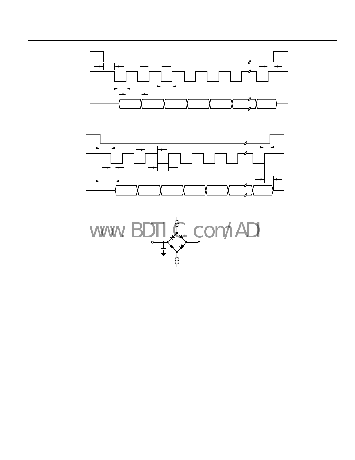
Page 5
ADIS16130
SCLK
www.BDTIC.com/ADI
CS
t
11
SCLK
t
12
t
13
SDI MSB LSB
t
14
t
15
t
16
07238-002
Figure 2. Input Timing for Write Operation
CS
t
8
t
9
07238-003
SDO
t
4
t
5
t
5A
MSB LSB
t
6
t
7
Figure 3. Output Timing for Read Operation
(800µA AT DVDD = 5V
I
SINK
100µA AT DV
DD
= 3V)
TO OUTPUT
PIN
50pF
I
SOURCE
1.6V
(200µA AT DVDD = 5V
100µA AT DV
DD
= 3V)
07328-024
Figure 4. Load Circuit for Access Time and Bus Relinquish Time
Rev. A | Page 5 of 16
Page 6

ADIS16130
www.BDTIC.com/ADI
ABSOLUTE MAXIMUM RATINGS
Table 3.
Parameter Rating
Acceleration (Any Axis, Unpowered, 0.5 ms) 2000 g
Acceleration (Any Axis, Powered, 0.5 ms) 2000 g
+V
S
Output Short-Circuit Duration
(Any Pin to Common)
Operating Temperature Range −40°C to +85°C
Storage Temperature Range −65°C to +150°C
−0.3 V to +6.0 V
Indefinite
Stresses above those listed under Absolute Maximum Ratings
may cause permanent damage to the device. This is a stress
rating only; functional operation of the device at these or any
other conditions above those indicated in the operational
section of this specification is not implied. Exposure to absolute
maximum rating conditions for extended periods may affect
device reliability.
Dropping the device onto a hard surface may cause a shock of
reater than 2000 g and exceed the absolute maximum rating of
g
the device. Care should be exercised when handling the device
to avoid damage.
THERMAL RESISTANCE
The ADIS16130 provides a temperature output that is
representative of the junction temperature. This can be used
for system-level monitoring and power management/thermal
characterization.
Table 4. Thermal Characteristics
Package Type
24-Lead Module 15.7 1.48 °C/W
1
Weight = 28.5 g typical.
1
θ
RATE
AXIS
+
JA
θ
JC
POSITIVE
ROTATIO N
DIRECTIO N
Unit
07238-026
Figure 5. Rotational Measurement Orientation
ESD CAUTION
Rev. A | Page 6 of 16
Page 7

ADIS16130
www.BDTIC.com/ADI
PIN CONFIGURATION AND FUNCTION DESCRIPTIONS
ADIS16130
TOP VIEW
(Not to Scale)
STSTST
23456789101112131415161718192021222324
1
STSTSTSTST
CS
RDY
SDO
SDI
VCC
VCC
Figure 6. Pin Configuration
Table 5. Pin Function Descriptions
Pin No. Mnemonic Description
1 to 7, 9 ST Self-Test (see the Self-Test Function section)
8
10
CS
RDY
Chip Select of the SPI
Data Ready
11, 13, 15 VCC Power Supply
12 SDO Data Output of the SPI
14 SDI Data Input of the SPI
16 SCLK Serial Clock of the SPI
17, 19 to 22 GND Power Supply Ground
18
SYNC
Synchronization Input
23 ROA1 Analog Filter Node 1
24 ROA2 Analog Filter Node 2
SCLK
SYNC
GND
GND
ROA2
VCC
GND
GND
GND
07328-004
ROA1
Rev. A | Page 7 of 16
Page 8

ADIS16130
www.BDTIC.com/ADI
TYPICAL PERFORMANCE CHARACTERISTICS
2.5
2.0
1.5
1.0
0.5
0
–0.5
BIAS SHIFT (°/sec)
–1.0
–1.5
–2.0
–2.5
–60 –40 –20 0 20 40 60 80 100 120
TEMPERATURE ( °C)
σ
µ
σ
Figure 7. Bias Shift vs. Temperature, VCC = 5 V
07328-018
0.01
µ+ σ
ROOT ALL EN VARIANCE (° /sec)
0.001
1 10010 1000
INTEGRAT ION TI ME, (sec)
µ
µ – σ
Figure 10. Root Allen Variance, VCC = 5 V, 25°C
07328-021
1.00
0.75
0.50
0.25
0
–0.25
SENSITIV ITY ERROR (%)
–0.50
–0.75
–1.00
–60 –40 –20 0 20 40 60 80 100 120
TEMPERATURE ( °C)
Figure 8. Sensitivity Error vs. Temperature, VCC = 5 V
0.05
0
–0.05
2
1
0
SENSITIV ITY ERROR (%)
–1
07328-019
–2
0 50 100 150 200 250 300 350 400
ANGULAR RATE (° /sec)
07328-022
Figure 11. Sensitivity Error vs. Angular Rate, VCC = 5 V, 25°C
90
85
80
75
SENSITIV ITY ERROR (%)
–0.10
–0.15
4.75 5.0 5.25
POWER SUPPLY (V)
07328-020
Figure 9. Sensitivity Error vs. Power Supply, 25°C
Rev. A | Page 8 of 16
70
SELF-TEST RESPONSE (°/sec)
65
60
–60 –40 –20 0 20 40 80
TEMPERATURE (°C)
60 100 120
Figure 12. Self-Test Response vs. Temperature, VCC = 5 V
07328-023
Page 9

ADIS16130
www.BDTIC.com/ADI
BASIC OPERATION
The ADIS16130 produces digital angular rate (RATE) and
temperature (TEMP) data. The digital communication employs
a simple 4-wire SPI that provides access to output data and
several configuration features. A set of communication and
configuration registers govern the operation in the ADIS16130.
See
Tabl e 8 for a summary of these registers.
QUICK START
The ADIS16130 SPI operates in 8-bit segments. The first byte of
a SPI sequence goes into the COM register, which contains the
read/write control bit and the address of the target register. When
writing information into control registers, the next byte contains
the configuration information. When reading output data, the
next one to three bytes contain the contents of the register selected.
Configuration Sequence
The sequence in Table 6 provides the recommended configuration
sequence. Tabl e 2 and Figure 2 provide the timing information
r each segment of this configuration sequence.
fo
Table 6. Configuration Sequence
Step SDI1Register Purpose
1 0x01 COM Start a write sequence for IOP.
2 0x38 IOP
3 0x28 COM
4 0x0A RATECS
5 0x30 COM
6 0x05 RATECONV Initialize the RATE conversion.
7 0x2A COM
8 0x0A TEMPCS
9 0x32 COM
10 0x05 TEMPCONV Initialize the TEMP conversion.
11 0x38 COM
12 0x22 MODE
1
The SDI column lists the hexadecimal code representation of the SDI bit
input sequence.
Configure the data-ready signal to
w when the RATEDATA and
pulse lo
TEMPDATA output registers
contain new data. The data-ready
signal goes high after reading
either of these registers.
Start a write sequence for the
TECS register.
RA
Enable and configure the
oscope data channel.
gyr
Start a write sequence for
TECONV register.
RA
Start a write sequence for the
register.
TEMPCS
Enable and configure the
emperature data channel.
t
Start a write sequence for
ONV.
TEMPC
Start a write sequence for the
egister.
MODE r
Establish the data output
esolution to 24 bits and start the
r
conversion process with the
RATEDATA channel.
Reading RATE Output Data
After the configuration sequence in Tab le 6 is complete, reading the
output data is very simple. The ADIS16130 converts the RATE
and TEMP data continuously. To better understand this process,
Figure 13 provides an example read sequence, and Tab l e 2 and
Figure 3 provide critical timing details for the output signal.
The first byte of the sequence uses SDI to establish a read of the
ATE output register. This is accomplished by writing 0x48 to the
R
COM register.
The most significant byte is first in the SDO sequence, followed
y the next significant, and then the least significant. When 16-bit
b
resolution is in use, only two bytes are output from the SDO during
the read sequence.
CS
SCLK
SDO
SDI
RDY
0x48
Figure 13. Read Sequence Example
The data-ready signal,
DATA
RDY
, indicates that unread data is
DATA DATA
07328-005
available on both RATE and TEMP output registers. After the
RATE or TEMP channel is read, the signal returns high, as
shown in
s
equentially, and each has a sample rate of 5.7 kSPS. The
Figure 13. The RATE and TEMP channels update
internal sample rate is not dependent on the SPI signals or read
rates. Using the data-ready signal to drive data collection helps
avoid losing data due to data collision, which is when a userdriven read cycle coincides with the internal update time. In
this case, the old data remains and the new data is lost.
If a lower sample rate meets system-level requirements, the
ta-ready signal can still be useful in facilitating SPI read
da
sequences. In this case, the data-ready signal pulses high for
approximately 26 μs before returning low and then repeats this
pattern at two times the internal sample rate. This signal can
feed a counter circuit (or firmware), which drives a processor
interrupt routine at a reduced sample rate.
Reading TEMP Output Data
Reading TEMP data requires a sequence that is very similar to
that of Figure 13, except that the initial SDI sequence must be
hanged from 0x48 to 0x4A. If the TEMP data is not used, Step 7
c
to Step 10 of the configuration sequence are not required.
Rev. A | Page 9 of 16
Page 10

ADIS16130
www.BDTIC.com/ADI
CONFIGURATION OPTIONS
Synchronization Input
SYNC
The
other devices in the system. When the
register (IOP) is set and the
does not process any conversions. Instead, it waits until the
SYNC
the conversion to start from a known point in time (for example,
the rising edge of the
Self-Test Function
The self-test function enables system-level diagnostic checks for the
entire ADIS16130 sensor/signal conditioning circuit. To activate
the self-test function, there must be a logic high signal on all
ST pins (see
in a r
with the limits specified in this data sheet, users can determine
the pass/fail criteria for system-level diagnostic routines.
For normal gyroscope operation, place a logic low input on
all S
ST pins to GND.
Analog Bandwidth
The typical −3 dB cutoff frequency for the ADIS16130 is
300 Hz, which is the combined response of two single-pole
filters, as shown in Figure 14. Pin ROA1 and Pin ROA2 provide
he opportunity for further bandwidth reduction in the first
t
filter stage, as shown in the following relationship:
where:
R = 25 kΩ.
C = 6800 pF
C
ext
The relationship between the −3 dB cutoff frequency and the
exter
Tabl e 7 .
pin can be used to synchronize the ADIS16130 with
SYNC
bit in the I/O port
SYNC
pin is low, the ADIS16130
pin goes high, and then starts the operation. This allows
SYNC
pin).
Tabl e 5). When activated, the self-test function results
ate measurement shift. By comparing the observed shift
T pins. For systems that do not require this feature, tie all
=
dB
−
3
2
1
()
CCRf+××π×
ext
.
is as defined in Figure 15 and Ta bl e 7.
nal capacitance of the ADIS16130 is shown in Figure 15 and
0
–1
–2
–3
–4
–5
–6
AMPLITUDE (dB)
–7
–8
–9
–10
1 10 100 1k 10k
Figure 15. Frequency Response: C
C
ext
= 0.15µF
FREQUENCY (Hz)
C
ext
= 0 μF vs. C
ext
= 0µF
= 0.15 μF
ext
07328-007
Table 7. Nominal Bandwidth for Standard Capacitor Values
C
(pF) BW (Hz) C
ext
(pF) BW (Hz) C
ext
(pF) BW (Hz)
ext
1000 276.8 10,000 198.9 100,000 52.2
1200 274.4 12,000 187.2 120,000 44.8
1500 270.9 15,000 172.1 150,000 37.0
1800 267.5 18,000 159.2 180,000
31.5
2200 263.1 22,000 144.7 220,000 26.3
2700 257.7 27,000 129.9 270,000
21.8
3300 251.6 33,000 115.7 330,000 18.1
3900 245.8 39,000 104.4 390,000
15.5
4300 242.1 43,000 97.9 430,000 14.1
4700 238.4 47,000 92.3 470,000
12.9
5100 234.9 51,000 87.2 510,000 12.0
5600 230.7 56,000 81.6 560,000
10.9
6200 225.8 62,000 75.8 620,000 9.9
7500 215.8 75,000 65.6 750,000
8200 210.8 82,000 61.2 820,000
8.2
7.6
9100 204.7 91,000 56.3 910,000 6.8
327Hz 1kHz
Figure 14. Frequency Response Block Diagram
ADC
07328-006
Rev. A | Page 10 of 16
Page 11

ADIS16130
www.BDTIC.com/ADI
CONTROL REGISTERS
Table 8. Register Descriptions
Name Address Type Purpose
COM 0x00 W Facilitate communications in the SPI port (see Table 9)
IOP 0x01 R/W Data-ready and synchronization controls (see Table 10)
0x02 to 0x07 Reserved
RATEDATA 0x08 R Gyroscope output, rate of rotation
TEMPDATA 0x0A R Temperature output
0x10 to 0x22 Reserved
RATECS 0x28 R/W Gyroscope channel setup (see Table 11)
TEMPCS 0x2A R/W Temperature channel setup (see Table 12)
RATECONV 0x30 R/W Gyroscope conversion time control (see Table 13)
TEMPCONV 0x32 R/W Temperature conversion time control (see Table 13)
0x33 to 0x37 Reserved
MODE 0x38 R/W Resolution mode control (see Table 14)
CONTROL REGISTER DETAILS
Table 9. COM Register Bit Assignments
Bit Description
[7] 0
[6]
1 = read;
ite
0 = wr
[5:0] Register address
Table 10. IOP Register Bit Assignments
Bit Description
[7:4] 0011
[3]
1 = data-ready signal low when unread data on all channels;
data-ready signal low when unread data on one channel
0 =
[2:1] 00
[0]
0 = synchronization disabled;
1 = synchr
Table 11. RATECS Register Bit Assignments
Bit Description
[7:4] 0000
[3]
1 = channel enable;
0 = channe
[2:0] 010
onization enabled
l disable
Table 12. TEMPCS Register Bit Assignments
Bit Description
[7:4] 0000
[3]
1 = channel enable;
0 = channe
[2:0] 010
Table 13. RATECONV/TEMPCONV Bit Assignments
Bit Description
[7:0] 00000101
Table 14. MODE Register Bit Assignments
Bit Description
[7:2] 001000
[1]
1 = 24-bit resolution;
0 = 16-bit r
[0] 0
l disable
esolution
Rev. A | Page 11 of 16
Page 12

ADIS16130
C
0
www.BDTIC.com/ADI
APPLICATIONS INFORMATION
ACHIEVING OPTIMAL NOISE PERFORMANCE
Several system-level considerations can have an impact on the
noise and accuracy of the ADIS16130. Understanding and
managing these factors can influence the behavior of any high
performance system.
Supply and Common Considerations
The ADIS16130 provides approximately 1.8 μF of decoupling
capacitance. This capacitance is distributed throughout the
device and should be taken into account when considering
potential noise threats on the power supply lines.
Bandwidth Setting
If C
is applied to reduce the bandwidth of the ADIS16130
OUT
response, it should be placed close to the device. Long cable
leads and PCB traces increase the risk of introducing noise into
the system.
SECOND-LEVEL ASSEMBLY
The ADIS16130 package supports two mounting approaches:
a bulkhead mount, where the interface is separate from the
attachment surface, and a PCB mount that provides the
mechanical and electrical connections on the same surface.
Figure 16 provides a suggested design for the ADIS16130’s
echanical attachment. The hole pattern shown in Figure 16
m
ca
n support either mounting approach and enables the integration
of the mating socket layout that is illustrated in
The mating socket layout uses the Samtec CLM-112-02 family of
co
nnectors. The 24 holes that are inside the pad accommodate the
pins on the ADIS16130, which can extend beyond the package
body. The stress relief provided by these holes is important for
maintaining reliability and optimal bias stability performance.
Figure 17.
15.600 BSC
39.60 BSC
19.800 BSC
4x 2.500 BSC
0.019685
[0.5000]
(TYP)
.054 [1.37]
0.022± DIA (T YP)
NONPLATED
THRU HOLE 2×
Figure 17. Mating Socket Recommended Pad Layout with
31.200 BS
2x 0.560 BSC
ALIGNMENT HOLES
17.520
2.280
5.00 BSC
Figure 16. Suggested Hole Pattern for Mounting
0.4334 [11.0]
0.022 DIA THRU HO LE (TYP)
NONPLATED T HRU HOLE
Dim
ensions Shown in Inches and (Millimeters)
FOR MATING SOCKET
5.00 BSC
0.0240 [0.610]
0.0394 [1.00]
0.0394 [1.00]
0.1800
[4.57]
07238-025
7328-017
Rev. A | Page 12 of 16
Page 13

ADIS16130
www.BDTIC.com/ADI
OUTLINE DIMENSIONS
35.854
35.600
35.346
31.350
31.200
31.050
15.700
2.200
TYP
15.600
15.500
2.400 THRU HOL E
(4 PLACES)
39.750
39.600
39.450
2.200 TYP
3.27
3.07
2.87
44.254
44.000
43.746
010908-A
14.054
13.800
13.546
17.670
17.520
17.370
19.900
19.800
19.700
1.00 BSC
(LEAD PITCH)
5.50 BSC
TOP VIEW
END VIEW
0.30 BSC SQ
(PIN SIZE)
Figure 18. PCB Module with Connector Interface
(M
L-24-3)
Dimensions shown in millimeters
ORDERING GUIDE
Model Temperature Range Package Description Package Option
ADIS16130AMLZ
1
Z = RoHS Compliant Part.
1
−40°C to +85°C PCB Module with Connector Interface ML-24-3
Rev. A | Page 13 of 16
Page 14

ADIS16130
www.BDTIC.com/ADI
NOTES
Rev. A | Page 14 of 16
Page 15

ADIS16130
www.BDTIC.com/ADI
NOTES
Rev. A | Page 15 of 16
Page 16

ADIS16130
www.BDTIC.com/ADI
NOTES
©2008 Analog Devices, Inc. All rights reserved. Trademarks and
registered trademarks are the property of their respective owners.
D07238-0-3/08(A)
Rev. A | Page 16 of 16
 Loading...