

Page 1
Low Voltage, 300 MHz Quad 2:1 Mux Analog
FEATURES
Bandwidth: 300 MHz
Low insertion loss and on resistance: 5 Ω typical
On resistance flatness: 0.68 Ω typical
Single 3 V/5 V supply operation
Low quiescent supply current: 1 nA typical
Fast switching times:
, 7 ns
t
ON
t
, 5 ns
OFF
TTL/CMOS compatible
APPLICATIONS
RGB switches
HDTV
DVD-R
Audio/video switches
GENERAL DESCRIPTION
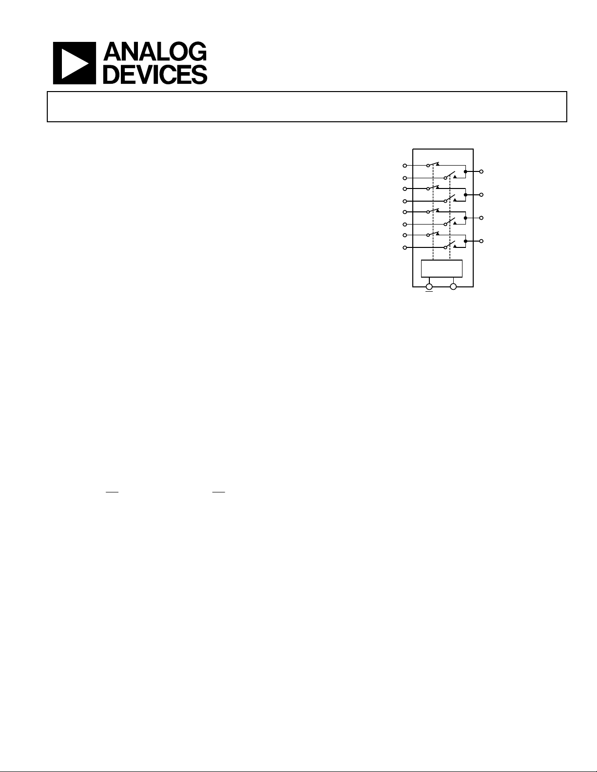
The ADG794 is a monolithic CMOS device comprising four
2:1 multiplexer/demultiplexers with high impedance outputs.
The CMOS process provides low power dissipation yet gives
high switching speed and low on resistance. The on resistance
variation is typically less than 1.2 Ω over the input signal range.
The bandwidth of the ADG794 is typically 300 MHz and this,
coupled with low distortion (typically 0.68%), makes the part
suitable for switching analog audio/video signals.
HDTV Audio/Video Switch
ADG794
FUNCTIONAL BLOCK DIAGRAM
S1A
S1B
S2A
S2B
S3A
S3B
S4A
S4B
These switches conduct equally well in both directions when on.
In the off condition, signal levels up to the supplies are blocked.
The ADG794 switches exhibit break-before-make switching
action.
The ADG794 is available in a 16-pin QSOP package.
PRODUCT HIGHLIGHTS
1. Wide bandwidth: 300 MHz.
ADG794
1 OF 2
DECODER
EN
Figure 1.
D1
D2
D3
D4
IN
05150-001
The ADG794 operates from a single 3.3 V/5 V supply and is
TTL logic compatible. The switches are controlled by the logic
EN
inputs IN and
as shown in Table 4. The EN pin allows the
user to disable all switches.
Rev. 0
Information furnished by Analog Devices is believed to be accurate and reliable.
However, no responsibility is assumed by Analog Devices for its use, nor for any
infringements of patents or other rights of third parties that may result from its use.
Specifications subject to change without notice. No license is granted by implication
or otherwise under any patent or patent rights of Analog Devices. Trademarks and
registered trademarks are the property of their respective owners.
2. Ultralow power dissipation.
3. Crosstalk is typically −70 dB at 10 MHz.
4. Off isolation is typically −65 dB at 10 MHz.
One Technology Way, P.O. Box 9106, Norwood, MA 02062-9106, U.S.A.
Tel: 781.329.4700
Fax: 781.326.8703 © 2004 Analog Devices, Inc. All rights reserved.
www.analog.com
Page 2

ADG794
TABLE OF CONTENTS
Specifications..................................................................................... 3
Typical Perfor m a n c e Character i stics ..............................................8
Single Supply ................................................................................. 3
Absolute Maximum Ratings............................................................ 5
ESD Caution.................................................................................. 5
Pin Configuration and Function Descriptions............................. 6
Te r m in o l o g y ...................................................................................... 7
REVISION HISTORY
10/04—Revision 0: Initial Version
Typical Application .......................................................................8
Tes t Ci rc u it s ........................................................................................9
Outline Dimensions....................................................................... 11
Ordering Guide .......................................................................... 11
Rev. 0 | Page 2 of 12
Page 3
ADG794
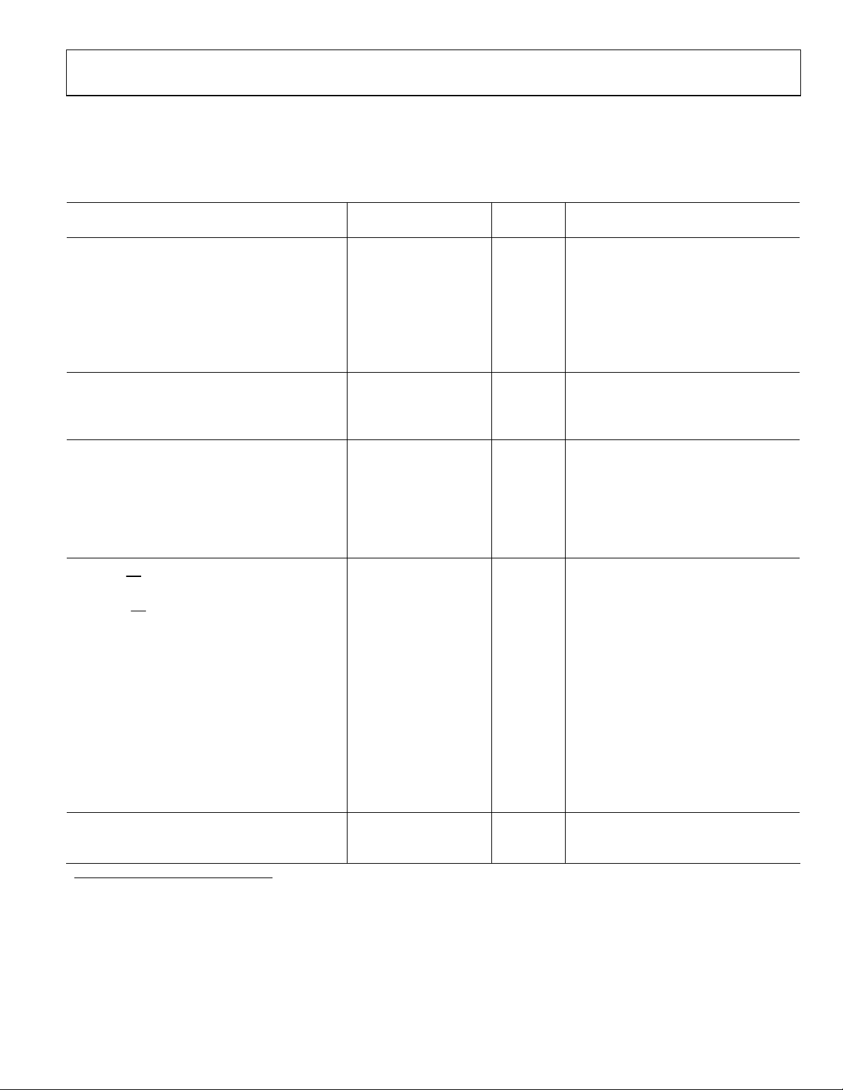
SPECIFICATIONS
SINGLE SUPPLY
VDD = 5 V ± 10%, GND = 0 V. All specifications T
Table 1.
Parameter 25°C T
ANALOG SWITCH
Analog Signal Range 0 to 2.5 V
On Resistance (RON) 5 Ω typ VD = 0 V to 1 V; IS = −10 mA; Figure 6
7 8 Ω max
On Resistance Match between Channels (∆RON) 0.4 Ω typ VD = 0 V to 1 V; IS = −10 mA
1.2 Ω max
On Resistance Flatness (R
) 0.7 Ω typ VD = 0 V to 1 V; IS = −10 mA
FLAT(ON)
1.35 Ω max
LEAKAGE CURRENTS
Source Off Leakage, IS (Off) ±0.001 nA typ VS = 3 V/1 V; VD = 1 V/3 V; Figure 7
Drain Off Leakage, ID (Off) ±0.001 nA typ VS = 3 V/1 V; VD = 1 V/3 V; Figure 7
Channel On Leakage, ID, IS (On) ±0.001 nA typ VD = VS = 3 V/1 V; Figure 8
DIGITAL INPUTS
Input High Voltage, V
Input Low Voltage, V
INH
INL
Input Current
I
or I
INL
INH
±0.1 µA max
Digital Input Capacitance, C
DYNAMIC CHARACTERISTICS
IN
2
tON, tON (EN)
14 ns max VS = 2 V; Figure 9
t
, t
(EN)
OFF
OFF
8 ns max VS = 2 V; Figure 9
Break-Before-Make Time Delay, t
D
1 ns min VS1 = VS2 = 2 V; Figure 10
Off Isolation −65 dB typ f = 10 MHz; RL = 50 Ω; Figure 12
Channel-to-Channel Crosstalk −70 dB typ f = 10 MHz; RL = 50 Ω; Figure 13
Bandwidth −3 dB 300 MHz typ RL = 50 Ω; Figure 11
Distortion 0.7 % typ RL = 100 Ω
Charge Injection 6 pC typ CL = 1 nF; VS = 0 V; Figure 14
CS (Off) 6 pF typ
CD (Off) 7.5 pF typ
CD, CS (On) 13.5 pF typ
POWER REQUIREMENTS VDD = 5.5 V; digital inputs = 0 V or V
I
DD
1 µA max
1
Temperature range for B Version is −40°C to +85°C.
2
Guaranteed by design, not subject to production test.
MIN
to T
, unless other wise no ted.
MAX
MIN
1
to T
MAX
B Version
Unit Test Conditions/Comments
2.4 V min
0.8 V max
0.001 µA typ VIN = V
INL
or V
3 pF typ
7 ns typ C
5 ns typ C
= 35 pF; RL = 50 Ω
L
= 35 pF; RL = 50 Ω
L
3 ns typ CL = 35 pF; RL = 50 Ω
0.001 µA typ
INH
DD
Rev. 0 | Page 3 of 12
Page 4

ADG794
VDD = 3 V ± 10%, GND = 0 V. All specifications T
Table 2.
B Version
Parameter 25°C T
ANALOG SWITCH
Analog Signal Range 0 to 1.5 V
On Resistance (RON) 7 Ω typ VD = 0 V to 1 V; IS = −10 mA; Figure 6
9.5 11 Ω max
On Resistance Match between Channels (∆RON)
0.9 Ω max
On Resistance Flatness (R
) 2.6 Ω typ VD = 0 V to 1 V; IS = −10 mA
FLAT(ON)
5 Ω max
LEAKAGE CURRENTS
Source Off Leakage, IS (Off) ±0.001 nA typ VS = 2 V/1 V; VD = 1 V/2 V; Figure 7
Drain Off Leakage, ID (Off) ±0.001 nA typ VS = 2 V/1 V; VD = 1 V/2 V; Figure 7
Channel On Leakage, ID, IS (On) ±0.001 nA typ VD = VS = 2 V/1 V; Figure 8
DIGITAL INPUTS
Input High Voltage, V
Input Low Voltage, V
INH
INL
Input Current
I
or I
INL
INH
±0.1 µA max
Digital Input Capacitance, C
DYNAMIC CHARACTERISTICS
IN
2
tON, tON (EN)
16 ns max VS = 1.5 V; Figure 9
t
, t
(EN)
OFF
OFF
10 ns max VS = 1.5 V; Figure 9
Break-Before-Make Time Delay, t
D
1 ns min VS1 = VS2 = 1.5 V; Figure 10
Off Isolation −65 dB typ f = 10 MHz; RL = 50 Ω; Figure 12
Channel-to-Channel Crosstalk −70 dB typ f = 10 MHz; RL = 50 Ω; Figure 13
Bandwidth −3 dB 300 MHz typ RL = 50 Ω; Figure 11
Distortion 2.6 % typ RL = 100 Ω
Charge Injection 4 pC typ CL = 1 nF; VS = 0 V; Figure 14
CS (Off) 6 pF typ
CD (Off) 7.5 pF typ
CD, CS (On) 13.5 pF typ
POWER REQUIREMENTS VDD = 3.3 V; digital inputs = 0 V or V
I
DD
1 µA max
1
Temperature range for B Version is −40°C to +85°C.
2
Guaranteed by design, not subject to production test.
MIN
to T
, unless other wise no ted.
MAX
1
to T
MIN
Unit Test Conditions/Comments
MAX
0.3 Ω typ VD = 0 V to 1 V; IS = −10 mA
2.0 V min
0.4 V max
0.001 µA typ VIN = V
INL
or V
3 pF typ
8 ns typ C
6 ns typ C
= 35 pF; RL = 50 Ω
L
= 35 pF; RL = 50 Ω
L
3 ns typ CL = 35 pF; RL = 50 Ω
0.001 µA typ
INH
DD
Rev. 0 | Page 4 of 12
Page 5

ADG794
ABSOLUTE MAXIMUM RATINGS
TA = 25°C, unless otherwise noted.
Table 3.
Parameters Ratings
VDD to GND −0.3 V to +6 V
Analog, Digital Inputs
Continuous Current, S or D 100 mA
Peak Current, S or D
Operating Temperature Range
Industrial (B Version) −40°C to +85°C
Storage Temperature Range −65°C to +150°C
Junction Temperature 150°C
QSOP Package, Power Dissipation 566 mW
θJA Thermal Impedance 149.97°C/W
Lead Temperature, Soldering
Vapor Phase (60 s) 215°C
Infrared (15 s) 220°C
1
−0.3 V to VDD + 0.3 V or
30 mA, whichever occurs
first
300 mA (pulsed at 1 ms,
10% duty cycle max)
1
Overvoltages at IN, S, or D are clamped by internal diodes. Current should be
limited to the maximum ratings given.
Stresses above those listed under Absolute Maximum Ratings
may cause permanent damage to the device. This is a stress
rating only; functional operation of the device at these or any
other conditions above those listed in the operational sections
of this specification is not implied. Exposure to absolute
maximum rating conditions for extended periods may affect
device reliability. Only one absolute maximum rating may be
applied at any one time.
Table 4. Truth Table
EN
1 X Hi-Z Hi-Z Hi-Z Hi-Z Disable
0 0 S1A S2A S3A S4A IN = 0
0 1 S1B S2B S3B S4B IN = 1
IN D1 D2 D3 D4 Function
ESD CAUTION
ESD (electrostatic discharge) sensitive device. Electrostatic charges as high as 4000 V readily accumulate on the
human body and test equipment and can discharge without detection. Although this product features
proprietary ESD protection circuitry, permanent damage may occur on devices subjected to high energy
electrostatic discharges. Therefore, proper ESD precautions are recommended to avoid performance
degradation or loss of functionality.
Rev. 0 | Page 5 of 12
Page 6

ADG794
PIN CONFIGURATION AND FUNCTION DESCRIPTIONS
1
IN
2
S1A
3
S1B
S2A
S2B
GND D3
D1
D2
ADG794
TOP VIEW
4
(Not to Scale)
5
6
7
8
16
V
DD
15
EN
14
S4A
13
S4B
12
D4
11
S3A
10
S3B
9
05150-002
Figure 2. Pin Configuration
Table 5. Pin Function Descriptions
Pin Number Mnemonic Description
1 IN Logic Control Input. The logic level at this input controls the operation of the multiplexers (see Table 4).
2 S1A A-Side Source Terminal of MUX1. Can be an input or output.
3 S1B B-Side Source Terminal of MUX1. Can be an input or output.
4 D1 Drain Terminal of MUX1. Can be an input or output.
5 S2A A-Side Source Terminal of MUX2. Can be an input or output.
6 S2B B-Side Source Terminal of MUX2. Can be an input or output.
7 D2 Drain Terminal of MUX2. Can be an input or output.
8 GND Ground Reference.
9 D3 Drain Terminal of MUX3. Can be an input or output.
10 S3B B-Side Source Terminal of MUX3. Can be an input or output.
11 S3A A-Side Source Terminal of MUX3. Can be an input or output.
12 D4 Drain Terminal of MUX4. Can be an input or output.
13 S4B B-Side Source Terminal of MUX4. Can be an input or output.
14 S4A A-Side Source Terminal of MUX4. Can be an input or output.
15
16 V
EN
DD
MUX Enable Logic Input. Enables or disables the multiplexers (see Table 4).
Positive Power Supply Voltage.
Rev. 0 | Page 6 of 12
Page 7

ADG794
TERMINOLOGY
VDD
Most positive power supply potential.
I
DD
Positive supply current.
GND
Ground (0 V) reference.
S
Source terminal. Can be either an input or an output.
D
Drain terminal. Can be either an input or an output.
IN
Logic control input.
(VS)
V
D
Analog voltage on terminals D, S.
R
ON
Ohmic resistance between D and S.
R
FLAT (ON)
Flatness is defined as the difference between the maximum and
minimum value of on resistance as measured.
∆R
ON
On resistance match between any two channels.
(Off)
I
S
Source leakage current with the switch off.
(Off)
I
D
Drain leakage current with the switch off.
, IS (On)
I
D
Channel leakage current with the switch on.
V
INL
Maximum input voltage for Logic 0.
V
INH
Minimum input voltage for Logic 1.
(I
INL
INH
)
I
Input current of the digital input.
(Off)
C
S
Off switch source capacitance. Measured with reference to
ground.
C
(Off)
D
Off switch drain capacitance. Measured with reference to
ground.
C
, CS (On)
D
On switch capacitance. Measured with reference to ground.
C
IN
Digital input capacitance.
t
ON
Delay time between the 50% and the 90% points of the digital
input and switch on condition.
t
OFF
Delay time between the 50% and the 90% points of the digital
input and switch off condition.
t
BBM
On or off time measured between the 80% points of both
switches when switching from one to another.
Charge Injection
A measure of the glitch impulse transferred from the digital
input to the analog output during on/off switching.
Off Isolation
A measure of unwanted signal coupling through an off switch.
Crosstalk
A measure of unwanted signal that is coupled through from one
channel to another as a result of parasitic capacitance.
−3 dB Bandwidth
The frequency at which the output is attenuated by 3 dB.
On Response
The frequency response of the on switch.
Insertion Loss
The loss due to the on resistance of the switch.
THD + N
The ratio of the harmonic amplitudes plus noise of a signal to
the fundamental.
Rev. 0 | Page 7 of 12
Page 8

ADG794
TYPICAL PERFORMANCE CHARACTERISTICS
0
0
–20
–40
–60
ATTENUATION (dB)
–80
–100
0.01
0.1 1 10 100 1000
Figure 3. Off Is olation vs. Fre quency
TYPICAL APPLICATION
FREQUENCY (MHz)
SIGNAL SOURCE
AUDIO/SYNC/OTHER
SIGNAL SOURCE 1
RGB VIDEO
1
–20
–40
–60
ATTENUATION (dB)
–80
05150-003
–100
0.01
0.1 1 10 100 1000
FREQUENCY (MHz)
05150-004
Figure 4. Crosstalk vs. Frequenc y
ADG794
R
G
B
R
R OUTPUT
G OUTPUT
B OUTPUT
AUDIO/SYNC/
OTHER OUTPUT
RGB VIDEO
SIGNAL SOURCE
2
AUDIO/SYNC/OTHER
SIGNAL SOURCE 2
G
B
EN
Figure 5. Audio/Video Switch
Rev. 0 | Page 8 of 12
IN
05150-005
Page 9

ADG794
V
V
TEST CIRCUITS
I
DS
V1
SD
V
S
RON = V1/I
DS
05150-006
IS (OFF) ID (OFF)
SD
A
V
S
A
V
D
05150-007
NC
SD
NC = NO CONNECT
Figure 6. On Resistance Figure 7. Off Leakage Figure 8. On Leakage
5V
0.1µF
3V
V
V
DD
V
C
L
35pF
OUT
SD
V
S
IN
GND
EN
R
L
100Ω
IN
V
OUT
50% 50%
90% 90%
t
ON
t
OFF
05150-009
Figure 9. Switching Times
5V
0.1µF
V
DD
S1A
S1B
S
V
EN
S
DECODER
IN
GND
D1
R
L
100Ω
V
C
L
35pF
OUT
3V
V
IN
0V
V
OUT
V
S
50% 50%
50% 50%
t
D
t
D
ID (ON)
A
V
D
05150-008
05150-010
Figure 10. Break-Before-Make Time Delay
V
DD
0.1µF
ADG794
S1A
IN
IN
EN
D1
GND
NETWORK
ANALYZER
50Ω
V
S
V
OUT
50Ω
05150-011
Figure 11. Bandwidth
Rev. 0 | Page 9 of 12
Page 10

ADG794
V
0.1µF
V
DD
ADG794
S1A
IN
IN
EN
GND
50Ω
D1
NETWORK
ANALYZER
50Ω
V
S
V
50Ω
OUT
05150-012
Figure 12. Off Isolation
V
DD
0.1µF
ADG794
S1A
S2A
IN
D2
V
IN
EN
D1
GND
50Ω
50Ω
NETWORK
ANALYZER
50Ω
V
OUT
R
L
50Ω
V
S
05150-013
Figure 13. Channel-to-Channel Crosstalk
5V
V
DD
R
S
V
S
S1A
S1B
S2A
S2B
S3A
S3B
S4A
S4B
ADG794
1 OF 2
DECODER
EN
D1 V
D2 V
D3 V
D4 V
OUT
OUT
OUT
OUT
C
L
1nF
C
L
1nF
C
L
1nF
C
L
1nF
IN
3V
V
EN
V
OUT
Q
= CL×∆V
INJ
OUT
∆V
OUT
05150-014
Figure 14. Charge Injection
Rev. 0 | Page 10 of 12
Page 11

Preliminary Technical Data ADG794
OUTLINE DIMENSIONS
0.193 (4.90)
BSC
16
1
0.065 (1.65)
0.049 (1.24)
0.010 (0.25)
0.004 (0.10)
COPLANARITY
0.004 (0.10)
CONTROLLING DIMENSIONS ARE IN INCHES; MILLIMETERS DIMENSIONS
(IN PARENTHESES) ARE ROUNDED-OFF MILLIMETER EQUIVALENTS FOR
REFERENCE ONLY AND ARE NOT APPROPRIATE FOR USE IN DESIGN
PIN 1
0.025 (0.14)
BSC
COMPLIANT TO JEDEC STANDARDS MO-137AB
9
8
0.012 (0.30)
0.008 (0.20)
0.154
(3.91)
BSC
0.069 (1.75)
0.053 (1.35)
SEATING
PLANE
0.236
(5.99)
BSC
0.010 (0.25)
0.006 (0.15)
8°
0°
0.050 (1.27)
0.016 (0.41)
Figure 15. 16-Lead Shrink Small Outline Package [QSOP]
(RQ-16)
Dimensions shown in inches and (millimeters)
ORDERING GUIDE
Model Temperature Range Package Description Package Option
ADG794BRQZ
ADG794BRQZ-500RL71
ADG794BRQZ-REEL1
ADG794BRQZ-REEL71
1
Z = Pb-free part.
1
−40°C to +85°C
−40°C to +85°C
−40°C to +85°C
−40°C to +85°C
16-Lead Shrink Small Outline Package (QSOP) RQ-16
16-Lead Shrink Small Outline Package (QSOP) RQ-16
16-Lead Shrink Small Outline Package (QSOP) RQ-16
16-Lead Shrink Small Outline Package (QSOP) RQ-16
Rev. 0 | Page 11 of 12
Page 12

ADG794
NOTES
© 2004 Analog Devices, Inc. All rights reserved. Trademarks and
registered trademarks are the property of their respective owners.
D05150–0–10/04(0)
Rev. 0 | Page 12 of 12
 Loading...