

Page 1
CMOS, 1.8 V to 5.5 V/±2.5 V, 3 Ω
S1S
www.BDTIC.com/ADI
FEATURES
1.8 V to 5.5 V single supply
±2.5 V dual supply
3 Ω on resistance
0.75 Ω on resistance flatness
100 pA leakage currents
14 ns switching times
Single 8-to-1 multiplexer ADG708
Differential 4-to-1 multiplexer ADG709
16-lead TSSOP package
Low power consumption
TTL-/CMOS-compatible inputs
APPLICATIONS
Data acquisition systems
Communication systems
Relay replacement
Audio and video switching
Battery-powered systems
Low Voltage 4-/8-Channel Multiplexers
ADG708/ADG709
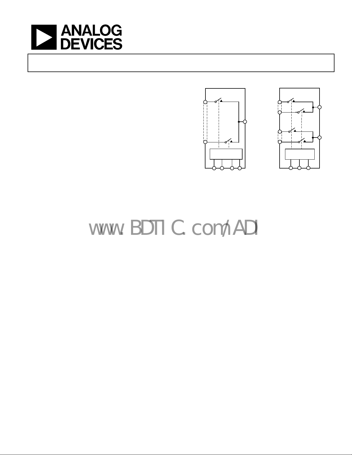
FUNCTIONAL BLOCK DIAGRAMS
ADG708
S1A
S4A
S1B
8
1 OF 8
DECODER
A0DA1 A2
Figure 1. Figure 2.
EN
S4B
00041-001
ADG709
1 OF 4
DECODER
A0
A1
EN
DA
DB
00041-002
GENERAL DESCRIPTION
The ADG708 and ADG709 are low voltage, CMOS analog
multiplexers comprising eight single channels and four
differential channels, respectively. The ADG708 switches one of
eight inputs (S1 to S8) to a common output, D, as determined
by the 3-bit binary address lines A0, A1, and A2. The ADG709
switches one of four differential inputs to a common differential
output as determined by the 2-bit binary address lines A0 and
A1. An EN input on both devices is used to enable or disable
the device. When disabled, all channels are switched off.
Low power consumption and an operating supply range of
1.8 V to 5.5 V make the ADG708 and ADG709 ideal for
battery-powered, portable instruments. All channels exhibit
break-before-make switching action preventing momentary
shorting when switching channels.
These switches are designed on an enhanced submicron process
that provides low power dissipation yet gives high switching
speed, very low on resistance, and leakage currents.
On resistance is in the region of a few ohms and is closely
matched between switches and very flat over the full signal
range. These parts can operate equally well as either multiplexers
or demultiplexers and have an input signal range that extends to
the supplies.
The ADG708 and ADG709 are available in 16-lead TSSOP
packages.
PRODUCT HIGHLIGHTS
1. Single-/dual-supply operation. The ADG708 and ADG709
are fully specified and guaranteed with 3 V and 5 V single
supply and ±2.5 V dual-supply rails.
2. Low R
3. Low power consumption (<0.01 μW).
4. Guaranteed break-before-make switching action.
5. Small 16-lead TSSOP package.
(3 Ω typical).
ON
Rev. B
Information furnished by Analog Devices is believed to be accurate and reliable. However, no
responsibility is assumed by Anal og Devices for its use, nor for any infringements of patents or ot her
rights of third parties that may result from its use. Specifications subject to change without notice. No
license is granted by implication or otherwise under any patent or patent rights of Analog Devices.
Trademarks and registered trademarks are the property of their respective owners.
One Technology Way, P.O. Box 9106, Norwood, MA 02062-9106, U.S.A.
Tel: 781.329.4700 www.analog.com
Fax: 781.461.3113 ©2006 Analog Devices, Inc. All rights reserved.
Page 2

ADG708/ADG709
www.BDTIC.com/ADI
TABLE OF CONTENTS
Features.............................................................................................. 1
ESD Caution...................................................................................9
Applications....................................................................................... 1
Functional Block Diagrams............................................................. 1
General Description ......................................................................... 1
Product Highlights ........................................................................... 1
Revision History ............................................................................... 2
Specifications..................................................................................... 3
Dual Supply................................................................................... 7
Absolute Maximum Ratings............................................................ 9
REVISION HISTORY
8/06−Rev. A to Rev. B
Updated Format.................................................................. Universal
Changes to Absolute Maximum Ratings Section..........................9
Added Table 7 and Table 8 .............................................................10
Updated Outline Dimensions........................................................18
Changes to Ordering Guide...........................................................18
4/02—Rev. 0 to Rev. A
E
dits to FEATURES and PRODUCT HIGHLIGHTS..................1
Change to SPECIFICATIONS.................................................... 2–4
Edits to ABSOLUTE MAXIMUM RATINGS Notes ....................5
Edits to TPCs 2, 5, 6–9, 11, and 15............................................. 7–9
Edits to Test Circuits 9 and 10 .......................................................11
Addition of Test Circuit 11.............................................................11
Pin Configuration and Function Descriptions........................... 10
Terminology.................................................................................... 11
Typical Performance Characteristics........................................... 12
Test Circuits..................................................................................... 15
Power-Supply Sequencing......................................................... 17
Outline Dimensions....................................................................... 18
Ordering Guide............................................................................... 18
10/00—Revision 0: Initial Version
Rev. B | Page 2 of 20
Page 3
ADG708/ADG709
www.BDTIC.com/ADI
SPECIFICATIONS
VDD = 5 V ± 10%, VSS = 0 V, GND = 0 V, unless otherwise noted.
Table 1.
B Version C Version
−40°C to
Parameter +25°C
ANALOG SWITCH
Analog Signal Range 0 V to VDD 0 V to VDD V
On Resistance (RON) 3 3 Ω typ VS = 0 V to VDD, IDS = 10 mA;
4.5 5 4.5 5 Ω max see Figure 20
On Resistance Match Between 0.4 0.4 Ω typ
Channels (ΔRON) 0.8 0.8 Ω max VS = 0 V to VDD, IDS = 10 mA
On Resistance Flatness (R
1.2 1.2 Ω max
LEAKAGE CURRENTS VDD = 5.5 V
Source Off Leakage IS (OFF) ±0.01 ±0.01 nA typ VD = 4.5 V/1 V, VS = 1 V/4.5 V;
±20 ±0.1 ±0.3 nA max see Figure 21
Drain Off Leakage ID (OFF) ±0.01 ±0.01 nA typ VD = 4.5 V/1 V, VS = 1 V/4.5 V;
±20 ±0.1 ±0.75 nA max see Figure 22
Channel On Leakage ID, IS (ON) ±0.01 ±0.01 nA typ VD = VS = 1 V or 4.5 V; see Figure 23
±20 ±0.1 ±0.75 nA max
DIGITAL INPUTS
Input High Voltage, V
Input Low Voltage, V
Input Current
I
or I
0.005 0.005 μA typ VIN = V
INL
INH
±0.1 ±0.1 μA max
Digital Input Capacitance, CIN 2 2 pF typ
DYNAMIC CHARACTERISTICS2
t
25 25 ns max VS1 = 3 V/0 V, VS8 = 0 V/3 V
Break-Before-Make Time Delay, t
1 1 ns min VS = 3 V; see Figure 25
tON (EN) 14 14 ns typ RL = 300 Ω, CL = 35 pF
25 25 ns max VS = 3 V; see Figure 26
t
12 12 ns max VS = 3 V; see Figure 26
Charge Injection ±3 ±3 pC typ VS = 2.5 V, RS = 0 Ω, CL = 1 nF;
see Figure 27
Off Isolation −60 −60 dB typ RL = 50 Ω, CL = 5 pF, f = 10 MHz
−80 −80 dB typ RL = 50 Ω, CL = 5 pF, f = 1 MHz;
see Figure 28
Channel-to-Channel Crosstalk −60 −60 dB typ RL = 50 Ω, CL = 5 pF, f = 10 MHz
−80 −80 dB typ RL = 50 Ω, CL = 5 pF, f = 1 MHz;
see Figure 29
−3 dB Bandwidth 55 55 MHz typ RL = 50 Ω, CL = 5 pF; see Figure 30
CS (OFF) 13 13 pF typ f = 1 MHz
CD (OFF)
14 14 ns typ RL = 300 Ω, CL = 35 pF; see Figure 24
TRANSITION
(EN) 7 7 ns typ RL = 300 Ω, CL = 35 pF
OFF
ADG708 85 85 pF typ f = 1 MHz
ADG709 42 42 pF typ f = 1 MHz
INH
0.8 0.8 V max
INL
) 0.75 0.75 Ω typ VS = 0 V to VDD, IDS = 10 mA
FLAT(ON)
2.4 2.4 V min
8 8 ns typ RL = 300 Ω, CL = 35 pF
OPEN
+85°
1
−40°C to
C
+25°C
+85°C
Unit Test Conditions/Comments
or V
INH
INL
Rev. B | Page 3 of 20
Page 4
ADG708/ADG709
www.BDTIC.com/ADI
B Version C Version
−40°C to
Parameter +25°C
CD, CS (ON)
ADG708 96 96 pF typ f = 1 MHz
ADG709 48 48 pF typ f = 1 MHz
POWER REQUIREMENTS VDD = 5.5 V
IDD 0.001 0.001 μA typ Digital inputs = 0 V or 5.5 V
1.0 1.0 μA max
1
Temperature range is as follows: B Version and C Version: −40°C to +85°C.
2
Guaranteed by design, not subject to production test.
+85°C
+25°C
−40°C to
+85°C
Unit Test Conditions/Comments
Rev. B | Page 4 of 20
Page 5
ADG708/ADG709
www.BDTIC.com/ADI
VDD = 3 V ± 10%, VSS = 0 V, GND = 0 V, unless otherwise noted.
Table 2.
B Version C Version
−40°C to
+85°
Parameter +25°C
C
ANALOG SWITCH
Analog Signal Range 0 V to VDD 0 V to VDD V
On Resistance (RON) 8 8 Ω typ VS = 0 V to VDD, IDS = 10 mA;
11 12 11 12 Ω max see Figure 20
On Resistance Match Between 0.4 0.4 Ω typ VS = 0 V to VDD , IDS = 10 mA
Channels (ΔRON) 1.2 1.2 Ω max
LEAKAGE CURRENTS VDD = 3.3 V
Source Off Leakage IS (OFF) ±0.01 ±0.01 nA typ VS = 3 V/1 V, VD = 1 V/3 V;
±20 ±0.1 ±0.3 nA max see Figure 21
Drain Off Leakage ID (OFF) ±0.01 ±0.01 nA typ VS = 3 V/1 V, VD = 1 V/3 V;
±20 ±0.1 ±0.75 nA max see Figure 22
Channel On Leakage ID, IS (ON) ±0.01 ±0.01 nA typ VS = VD = 1 V or 3 V; see Figure 23
±20 ±0.1 ±0.75 nA max
DIGITAL INPUTS
Input High Voltage, V
Input Low Voltage, V
2.0 2.0 V min
INH
0.8 0.8 V max
INL
Input Current
I
or I
0.005 0.005 μA typ VIN = V
INL
INH
±0.1 ±0.1 μA max
Digital Input Capacitance, CIN 2 2 pF typ
DYNAMIC CHARACTERISTICS2
t
18 18 ns typ RL = 300 Ω, CL = 35 pF; see Figure 24
TRANSITION
30 30 ns max VS1 = 2 V/0 V, VS2 = 0 V/2 V
Break-Before-Make Time Delay, t
8 8 ns typ RL = 300 Ω, CL = 35 pF
OPEN
1 1 ns min VS = 2 V; see Figure 25
tON (EN) 18 18 ns typ RL = 300 Ω, CL = 35 pF
30 30 ns max VS = 2 V; see Figure 26
t
(EN) 8 8 ns typ RL = 300 Ω, CL = 35 pF
OFF
15 15 ns max VS = 2 V; see Figure 26
Charge Injection ±3 ±3 pC typ VS = 1.5 V, RS = 0 Ω, CL = 1 nF;
see Figure 27
Off Isolation −60 −60 dB typ RL = 50 Ω, CL = 5 pF, f = 10 MHz
−80 −80 dB typ RL = 50 Ω, CL = 5 pF, f = 1 MHz;
see Figure 28
Channel-to-Channel Crosstalk −60 −60 dB typ RL = 50 Ω, CL = 5 pF, f = 10 MHz
−80 −80 dB typ RL = 50 Ω, CL = 5 pF, f = 1 MHz;
see Figure 29
−3 dB Bandwidth 55 55 MHz typ RL = 50 Ω, CL = 5 pF; see Figure 30
CS (OFF) 13 13 pF typ f = 1 MHz
CD (OFF)
ADG708 85 85 pF typ f = 1 MHz
ADG709 42 42 pF typ f = 1 MHz
CD, CS (ON)
ADG708 96 96 pF typ f = 1 MHz
ADG709 48 48 pF typ f = 1 MHz
1
−40°C to
+25°C
Rev. B | Page 5 of 20
+85°C
Unit Test Conditions/Comments
or V
INH
INL
Page 6

ADG708/ADG709
www.BDTIC.com/ADI
B Version C Version
−40°C to
Parameter +25°C
POWER REQUIREMENTS VDD = 3.3 V
IDD 0.001 0.001 μA typ Digital inputs = 0 V or 3.3 V
1.0 1.0 μA max
1
Temperature ranges are as follows: B Version and C Version: −40°C to +85°C.
2
Guaranteed by design, not subject to production test.
+85°C
+25°C
−40°C to
+85°C
Unit Test Conditions/Comments
Rev. B | Page 6 of 20
Page 7

ADG708/ADG709
www.BDTIC.com/ADI
DUAL SUPPLY
VDD = +2.5 V ± 10%, V
Table 3.
B Version C Version
Parameter +25°C
ANALOG SWITCH
Analog Signal Range VSS to VDD VSS to VDD V
On Resistance (RON) 2.5 2.5 Ω typ VS = VSS to VDD, IDS = 10 mA;
4.5 5 4.5 5 Ω max see Figure 20
On Resistance Match Between 0.4 0.4 Ω typ
Channels (ΔRON) 0.8 0.8 Ω max VS = VSS to VDD, IDS = 10 mA
On Resistance Flatness (R
1.0 1.0 Ω max
LEAKAGE CURRENTS VDD = +2.75 V, VSS = −2.75 V
Source Off Leakage IS (OFF) ±0.01 ±0.01 nA typ VS = +2.25 V/−1.25 V, VD = −1.25 V/+2.25 V;
±20 ±0.1 ±0.3 nA max see Figure 21
Drain Off Leakage ID (OFF) ±0.01 ±0.01 nA typ VS = +2.25 V/−1.25 V, VD = −1.25 V/+2.25 V;
±20 ±0.1 ±0.75 nA max see Figure 22
Channel On Leakage ID, IS (ON) ±0.01 ±0.01 nA typ VS = VD = +2.25 V/−1.25 V; see Figure 23
±20 ±0.1 ±0.75 nA max
DIGITAL INPUTS
Input High Voltage, V
Input Low Voltage, V
Input Current
I
or I
0.005 0.005 μA typ VIN = V
INL
INH
±0.1 ±0.1 μA max
Digital Input Capacitance, CIN 2 2 pF typ
DYNAMIC CHARACTERISTICS2
t
14 14 ns typ RL = 300 Ω, CL = 35 pF; see Figure 24
TRANSITION
25 25 ns max VS = 1.5 V/0 V; see Figure 24
Break-Before-Make Time Delay, t
1 1 ns min VS = 1.5 V; see Figure 25
tON (EN) 14 14 ns typ RL = 300 Ω, CL = 35 pF
25 25 ns max VS = 1.5 V; see Figure 26
t
(EN) 8 8 ns typ RL = 300 Ω, CL = 35 pF
OFF
15 15 ns max VS = 1.5 V; see Figure 26
Charge Injection ±3 ±3 pC typ VS = 0 V, RS = 0 Ω, CL = 1 nF; see Figure 27
Off Isolation –60 –60 dB typ RL = 50 Ω, CL = 5 pF, f = 10 MHz
–80 –80 dB typ RL = 50 Ω, CL = 5 pF, f = 1 MHz; see Figure 28
Channel-to-Channel Crosstalk –60 –60 dB typ RL = 50 Ω, CL = 5 pF, f = 10 MHz
–80 –80 dB typ RL = 50 Ω, CL = 5 pF, f = 1 MHz; see Figure 29
−3 dB Bandwidth 55 55 MHz typ RL = 50 Ω, CL = 5 pF; see Figure 30
CS (OFF) 13 13 pF typ f = 1 MHz
CD (OFF)
ADG708 85 85 pF typ f = 1 MHz
ADG709 42 42 pF typ f = 1 MHz
CD, CS (ON)
ADG708 96 96 pF typ f = 1 MHz
ADG709 48 48 pF typ f = 1 MHz
= –2.5 V ± 10%, GND = 0 V, unless otherwise noted.1
SS
−40°C
to +85°C +25°C
0.6 0.6 Ω typ VS = VSS to VDD, IDS = 10 mA
FLAT(ON))
1.7 1.7 V min
INH
0.7 0.7 V max
INL
8 8 ns typ RL = 300 Ω, CL = 35 pF
OPEN
−40°C
to +85°C Unit Test Conditions/Comments
INL
or V
INH
Rev. B | Page 7 of 20
Page 8

ADG708/ADG709
www.BDTIC.com/ADI
B Version C Version
−40°C
Parameter +25°C
POWER REQUIREMENTS VDD = 2.75 V
IDD 0.001 0.001 μA typ Digital inputs = 0 V or 2.75 V
1.0 1.0 μA max
ISS 0.001 0.001 μA typ VSS = −2.75 V
1.0 1.0 μA max Digital inputs = 0 V or 2.75 V
1
Temperature range is as follows: B Version and C Version: −40°C to +85°C.
2
Guaranteed by design not subject to production test.
to +85°C
+25°C
−40°C
to +85°C
Unit Test Conditions/Comments
Rev. B | Page 8 of 20
Page 9

ADG708/ADG709
www.BDTIC.com/ADI
ABSOLUTE MAXIMUM RATINGS
TA = 25°C, unless otherwise noted.
Table 4.
Parameter Rating
VDD to VSS 7 V
VDD to GND −0.3 V to +7 V
VSS to GND +0.3 V to −3.5 V
Analog Inputs1
Digital Inputs1
Peak Current, S or D (Pulsed at 1 ms,
10% Duty Cycle Maximum)
Continuous Current, S or D 30 mA
Operating Temperature Range
Industrial (B and C Versions) −40°C to +85°C
Storage Temperature Range −65°C to +150°C
Junction Temperature 150°C
TSSOP Package, Power Dissipation 432 mW
θJA Thermal Impedance 150.4°C/W
θJC Thermal Impedance 27.6°C/W
Lead Temperature, Soldering
Vapor Phase (60 sec) 215°C
Infrared (15 sec) 220°C
1
Overvoltages at A, EN, S, or D are clamped by internal codes. Current should
be limited to the maximum ratings given.
− 0.3 V to VDD + 0.3 V
V
SS
or 30 mA, whichever
occurs first
−0.3 V to V
30 mA, whichever occurs
first
100 mA
+ 0.3 V or
DD
Table 5. ADG708 Truth Table
A2 A1 A0 EN Switch Condition
x1 x1 x1 0 NONE
0 0 0 1 1
0 0 1 1 2
0 1 0 1 3
0 1 1 1 4
1 0 0 1 5
1 0 1 1 6
1 1 0 1 7
1 1 1 1 8
1
x = don’t care.
Table 6. ADG709 Truth Table
A1 A0 EN ON Switch Pair
1
x
0 0 1 1
0 1 1 2
1 0 1 3
1 1 1 4
1
x = don’t care.
1
x
0 NONE
ESD CAUTION
Stresses above those listed under Absolute Maximum Ratings
may cause permanent damage to the device. This is a stress
rating only; functional operation of the device at these or any
other conditions above those indicated in the operational
section of this specification is not implied. Exposure to absolute
maximum rating conditions for extended periods may affect
device reliability.
Only one absolute maximum rating can be applied at any one time.
Rev. B | Page 9 of 20
Page 10

ADG708/ADG709
V
AS3AS4A
A
www.BDTIC.com/ADI
PIN CONFIGURATION AND FUNCTION DESCRIPTIONS
V
S1
S2
A0
EN
SS
DA
1
2
3
ADG709
4
TOP VIEW
5
(Not to Scale)
6
7
8
16
A1
15
GND
14
V
DD
13
S1B
12
S2B
11
S3B
S4B
10
9
DB
00041-004
A0
EN
SS
S1
S2
S3
S4
D
1
2
3
ADG708
4
TOP VIEW
5
(Not to Scale)
6
7
8
16
A1
15
A2
14
GND
V
13
DD
12
S5
11
S6
10
S7
9
S8
00041-003
Figure 3. ADG708 TSSOP Figure 4. ADG709 TSSOP
Table 7. ADG708 Pin Function Descriptions
Pin No. Mnemonic Description
1 A0 Digital Input. Controls the configuration of the switch, as shown in the truth table (see Table 5 ).
2 EN Digital Input. Controls the configuration of the switch, as shown in the truth table (see Tabl e 5).
3 V
SS
Most Negative Power Supply Pin in Dual Supply Applications. For single supply applications, it should be tied
to GND.
4 S1
5 S2
6 S3
7 S4
8 D
9 S8
10 S7
11 S6
12 S5
13 V
Most Positive Power Supply Pin.
DD
14 GND
15 A2
16 A1 Digital Input. Controls the configuration of the swit
Source Terminal. Can be an input or output.
Source Terminal. Can be an input or output.
Source Terminal. Can be an input or output.
Source Terminal. Can be an input or output.
Drain Terminal. Can be an input or output.
Source Terminal. Can be an input or output.
Source Terminal. Can be an input or output.
Source Terminal. Can be an input or output.
Source Terminal. Can be an input or output.
Ground (0 V) Reference.
Digital Input. Controls the configuration of the switch, as shown in the truth table (see Table 5).
ch, as shown in the truth table (see Table 5).
Table 8. ADG709 Pin Function Descriptions
Pin No. Mnemonic Description
1 A0 Digital Input. Controls the configuration of the switch, as shown in the truth table (see Tabl e 6).
2 EN Digital Input. Controls the configuration of the switch, as shown in the truth table (see Table 6).
3 V
SS
Most negative power supply pin in dual supply applications. For single supply applications, it should be tied
to GND.
4 S1A
5 S2A
6 S3A
7 S4A
8 DA
9 DB
10 S4B
11 S3B
12 S2B
13 S1B
14 V
Most Positive Power Supply Pin.
DD
15 GND
16 A1 Digital Input. Controls the configuration of the swit
Source Terminal. Can be an input or output.
Source Terminal. Can be an input or output.
Source Terminal. Can be an input or output.
Source Terminal. Can be an input or output.
Drain Terminal. Can be an input or output.
Drain Terminal. Can be an input or output.
Source Terminal. Can be an input or output.
Source Terminal. Can be an input or output.
Source Terminal. Can be an input or output.
Source Terminal. Can be an input or output.
Ground (0 V) Reference.
ch, as shown in the truth table (see Table 6).
Rev. B | Page 10 of 20
Page 11

ADG708/ADG709
www.BDTIC.com/ADI
TERMINOLOGY
VDD
Most positive power supply potential.
C
IN
Digital input capacitance.
VSS
Most negative power supply in a dual-supply application. In
sin
gle-supply applications, this should be tied to ground at the
device.
GND
Ground (0 V) reference.
S
Source terminal. Can be an input or output.
D
Drain terminal. Can be an input or output.
Ax
Logic control input.
EN
Active high enable.
R
ON
Ohmic resistance between D and S.
R
FLAT(ON)
Flatness is defined as the difference between the maximum and
minimum value of on resistance as measured over the specified
analog signal range.
I
(OFF)
S
Source leakage current with the switch off.
I
(OFF)
D
Drain leakage current with the switch off.
I
, IS (ON)
D
Channel leakage current with the switch on.
V
(VS)
D
Analog voltage on Terminal D and Terminal S.
C
(OFF)
S
Off switch source capacitance. Measured with reference to
round.
g
(OFF)
C
D
Off switch drain capacitance. Measured with reference to
round.
g
, CS (ON)
C
D
On switch capacitance. Measured with reference to ground.
t
TRANSITION
Delay time measured between the 50% and 90% points of the
dig
ital inputs and the switch on condition when switching from
one address state to another.
(EN)
t
ON
Delay time between the 50% and 90% points of the EN digital
input and the switch on condition.
t
(EN)
OFF
Delay time between the 50% and 90% points of the EN digital
input and the switch off condition.
t
OPEN
Off time measured between the 80% points of both switches
hen switching from one address state to another.
w
Off Isolation
A measure of unwanted signal coupling through an off switch.
Crosstalk
A measure of unwanted signal that is coupled through from one
nnel to another as a result of parasitic capacitance.
cha
Charge
A measure of the glitch impulse transferred from injection of
e digital input to the analog output during switching.
th
Bandwidth
The frequency at which the output is attenuated by 3 dB.
On Response
The frequency response of the on switch.
On Loss
The loss due to the on resistance of the switch.
V
INL
Maximum input voltage for Logic 0.
V
INH
Minimum input voltage for Logic 1.
I
(I
)
INL
INH
Input current of the digital input.
I
DD
Positive supply current.
I
SS
Negative supply current.
Rev. B | Page 11 of 20
Page 12

ADG708/ADG709
www.BDTIC.com/ADI
TYPICAL PERFORMANCE CHARACTERISTICS
8
7
6
5
4
3
ON RESISTANCE (Ω)
2
1
0
012345
VD OR VS – DRAIN OR SOURCE VOLTAGE (V)
Figure 5. On Resistance as a Function of V
8
7
6
5
4
3
ON RESISTANCE (Ω)
2
1
0
–2.5 –2.0 –1.5 –1.0 –0.5 1.0 1.5 2.0 2.5 3.00.50
–3.0
VD OR VS – DRAIN OR SOURCE VO LTAGE (V)
VDD = 2.7V
VDD = 3.3V
VDD = +2.25V
V
= –2.25V
SS
VDD = 4.5V
= +2.75V
V
DD
V
= –2.75V
SS
D
Figure 6. On Resistance as a Function of V
TA = 25°C
V
= 0V
SS
VDD= 5.5V
(VS) for Single Supply
= 25°C
T
A
(VS) for Dual Supply
D
8
7
6
5
4
3
ON RESISTANCE (Ω)
2
1
0
0 0.5 1.0 1.5 2.0 3.02.5
OR VS – DRAIN OR SOURCE VOLTAG E (V)
V
00041-005
D
Figure 8. On Resistance as a Function of V
–40°C
(VS) for Different Temperatures,
D
+85°C
+25°C
V
= 3V
DD
V
= 0V
SS
00041-008
Single Supply
8
7
6
5
4
3
ON RESISTANCE (Ω)
2
1
0
–3.0 –2.5 –2.0 –1.5 –1.0 0 0.5 1.0 1.5 2.0 2.5–0.5 3.0
OR VS – DRAIN OR SOURCE VO LTAGE (V)
V
00041-006
D
Figure 9. On Resistance as a Function of V
+85°C
–40°C
(VS) for Different Temperatures,
D
VDD = +2.5V
V
= –2.5V
SS
+25°C
0041-009
Dual Supply
8
7
6
5
4
3
ON RESISTANCE (Ω)
2
1
0
0123 4
VD OR VS – DRAIN OR SOURCE VOLTAGE (V)
Figure 7. On Resistance as a Function of V
+85°C
–40°C
(VS) for Different Temperatures,
D
+25°C
V
= 5V
DD
V
= 0V
SS
5
0041-007
Single Supply
Rev. B | Page 12 of 20
0.12
0.08
0.04
0
CURRENT (nA)
–0.04
–0.08
–0.12
012345
VS, (VD = VDD – VS) (V)
ID (ON)
IS (OFF)
Figure 10. Leakage Currents as a Function of V
VDD = 5V
V
SS
T
A
ID (OFF)
(VS)
D
= 0V
= 25°C
00041-010
Page 13

ADG708/ADG709
www.BDTIC.com/ADI
0.12
0.08
0.04
VDD = 3V
V
= 0V
SS
T
= 25°C
A
I
(ON)
D
0.35
0.30
0.25
0.20
VDD = 3V
V
= 0V
SS
0
CURRENT (nA)
–0.04
–0.08
–0.12
00.5
1.0 1.5 2.0 3.0
VD, (VS = VDD – VD) (V)
I
S
(OFF)
Figure 11. Leakage Currents as a Function of V
0.12
0.08
I
D
IS (OFF)
(ON), VS = V
ID (OFF)
CURRENT (nA)
–0.04
–0.08
–0.12
0.04
0
–3.0
–2.5 –2.0 –1.5 –1.0 0 0.5 1.0 1.5 2.0 2.5
–0.5 3.0
, (VD = VDD – VS) (V)
V
S
Figure 12. Leakage Currents as a Function of V
0.35
VDD = +5V
V
= 0V
SS
AND
0.30
V
= +2.5V
DD
V
= –2.5V
SS
0.25
0.20
0.15
CURRENT (nA)
–0.05
0.10
0.05
0
25 35 45 55 65 75 85
15
TEMPERATURE ( °C)
ID (OFF)
IS (OFF)
Figure 13. Leakage Currents as a Function of Temperature
(OFF)
I
D
2.5
(VS)
D
VDD = +2.5V
V
= –2.5V
SS
= 25°C
T
A
D
(VS)
D
ID (ON)
0.15
0.10
CURRENT (nA)
I
S
ID (OFF)
(OFF)
ID (ON)
00041-014
0.05
0
–0.05
0041-011
25 35 45 55 65 75 85
15
TEMPERATURE (°C)
Figure 14. Leakage Currents as a Function of Temperature
10m
TA = 25°C
1m
100µ
10µ
1µ
CURRENT (A)
100n
10n
1n
10
0041-012
00041-013
Figure 15. Supply Current vs. Input Switching Frequency
0
–20
–40
–60
–80
ATTENUATIO N (dB)
–100
–120
30k 100M10M100k 1M
Figure 16. Off Isolation vs. Fr
VDD= +2.5V
V
= –2.5V
SS
VDD = +3V
FREQUENCY (Hz)
FREQUENCY (Hz)
VDD = +5V
equency
V
DD
T
A
= 5V
= 25°C
10M1M10k 100k1k100
0041-015
00041-016
Rev. B | Page 13 of 20
Page 14

ADG708/ADG709
www.BDTIC.com/ADI
ATTENUATIO N (dB)
–100
–20
–40
–60
–80
0
VDD = 5V
T
= 25°C
A
20
10
0
= +3V
V
= +2.5V
= –2.5V
DD
V
= 0V
SS
(pC)
–10
INJ
Q
–20
–30
V
DD
V
SS
V
V
DD
SS
TA = 25°C
= +5V
= 0V
–120
ATTENUATION (dB)
–10
–15
–20
0
–5
30k
VDD = 5V
T
30k
FREQUENCY (Hz)
Figure 17. Crosstalk vs. Frequency
= 25°C
A
FREQUENCY (Hz)
100M10M100k 1M
0041-017
100M10M100k 1M
00041-018
–40
–3
–1 1 2 5
–2
VOLTAGE (V)
40
3
00041-019
Figure 19. Charge Injection vs. Source Voltage
Figure 18. On Response vs. Frequency
Rev. B | Page 14 of 20
Page 15

ADG708/ADG709
VSSV
VSSV
VSSV
*
V
V
V
V
www.BDTIC.com/ADI
TEST CIRCUITS
I
DS
V1
S
V
S
RON = V1/I
Figure 20. On Resistance
V
DD
V
I
V
(OFF)
S
S
A
V
D
DD
S1
S2
S8
Figure 21. I
DD
V
DD
A2
IN
50Ω
A1
A0
ADG708*
2.4V
SIMILAR CO NNECTION F OR ADG709.
V
IN
50Ω
EN
DD
V
DD
A2
A1
S2 TO S7
A0
ADG708*
2.4V
*SIMILAR CONNECTIO N FOR ADG709.
EN
GND
GND
(OFF)
S
GND
V
DS
V
SS
V
SS
EN
V
SS
S2 TO S7
SS
SS
S1
S8
D
D
0041-020
D
0.8V
00041-021
V
S1
S8
S1
V
S8
D
R
L
300Ω
C
L
35pF
V
OUT
Figure 24. Switching Time of Multiplexer, t
V
S
V
OUT
R
300Ω
C
L
L
35pF
Figure 25. Break-Before-Make Delay, t
ADDRESS
DRIVE (V
ADDRESS
DRIVE (V
DD
GND
Figure 22. I
DD
DD
Figure 23. I
90%
GND
t
V
OPEN
SS
I
(OFF)
D
D
A
V
90%
D
00041-022
V
D
00041-023
0041-024
00041-025
0.8V
EN
(OFF)
D
V
SS
I
(ON)
D
D
A
2.4V
EN
(ON)
D
50%
t
TRANSITI ON
80%
V
DD
S1
S2
S8
V
S
V
S1
S8
V
S
3V
t
TRANSITION
50%
80%
)
IN
0V
V
S1
V
OUT
V
S8
TRANSITION
3
)
IN
0V
V
OUT
OPEN
Rev. B | Page 15 of 20
Page 16

ADG708/ADG709
VDDV
V
V
V
V
2.4V
V
VDDV
www.BDTIC.com/ADI
ENABLE
DRIVE (V
OUTPUT
3
(V
IN
0V
V
OUT
)
3V
IN
0V
V
0V
ON
)
O
(EN), t
OFF
(EN)
50%
Q
INJ
0.9V
t
ON
= CL× ΔV
O
(EN)
OUT
50%
ΔV
OUT
0.9V
t
OFF
(EN)
O
0041-026
00041-027
SS
V
DDVSS
A2
A1
S2 TO S8
A0
ADG708*
EN
V
IN
50Ω
*SIMILAR CO NNECTION F OR ADG709.
R
S
V
S
V
IN
*SIMILAR CO NNECTION F OR ADG709.
GND
A2
A1
A0
S
EN
DD
V
DD
ADG708*
GND
V
S1
S
D
R
L
300Ω
C
L
35pF
V
OUT
Figure 26. Enable Delay, t
SS
V
LOGIC INPUT
OUT
V
SS
D
C
L
1nF
Figure 27. Charge Injection
0.1µF
OFF ISOLATION = 20 log
NETWORK
ANALYZER
50Ω
V
S
A2
A1
A0
EN
DD
SS
0.1µF
V
V
DD
SS
S
D
GND
50Ω
V
OUT
V
S
NETWORK
ANALYZER
50Ω
V
V
OUT
R
L
50Ω
S
00041-028
Figure 28. Off Isolation
V
DD
ADG708*
GND
SS
SS
EN
2.4V
NETWO RK
ANALYZER
D
R
50Ω
V
OUT
L
0.1µF 0.1µ F
V
A2
A1
A0
50Ω
S1
S2
S8
*SIMILAR CONNECTION FOR ADG709.
CHANNEL-TO-CHANNEL CROSSTALK = 20 log
Figure 29. Channel-to-Channel Crosstalk
Rev. B | Page 16 of 20
V
OUT
V
S
00041-029
Page 17

ADG708/ADG709
V
V
www.BDTIC.com/ADI
DD
V
DDVSS
S
GND
SS
D
0.1µF 0.1µF
A2
A1
A0
2.4V
INSERTION LOSS = 20 log
EN
Figure 30. Bandwidth
POWER-SUPPLY SEQUENCING
When using CMOS devices, care must be taken to ensure
correct power supply sequencing. Incorrect power supply
sequencing can result in the device being subjected to stresses
beyond the maximum ratings listed in the data sheet.
V
WITH SWITCH
OUT
V
WITHOUT SWITCH
OUT
NETWO RK
ANALYZER
50Ω
V
S
V
OUT
R
L
50Ω
0041-030
Digital and analog inputs should always be applied after power
su
pplies and ground. For single-supply operation, V
should be
SS
tied to GND as close to the device as possible.
Rev. B | Page 17 of 20
Page 18

ADG708/ADG709
www.BDTIC.com/ADI
OUTLINE DIMENSIONS
5.10
5.00
4.90
16
4.50
4.40
4.30
PIN 1
0.15
0.05
0.65
BSC
COPLANARITY
COMPLIANT TO JEDEC STANDARDS MO-153-AB
Figure 31. 16-Lead Thin Shrink S
0.10
0.30
0.19
9
81
1.20
MAX
SEATING
PLANE
6.40
BSC
0.20
0.09
8°
0°
mall Outline Package [TSSOP]
0.75
0.60
0.45
(RU-16)
Dimensions shown in millimeters
ORDERING GUIDE
Model Temperature Range Package Description Package Option
ADG708BRU −40°C to +85°C 16-Lead Thin Shrink Small Outline Package (TSSOP) RU-16
ADG708BRU-REEL −40°C to +85°C 16-Lead Thin Shrink Small Outline Package (TSSOP) RU-16
ADG708BRU-REEL7 −40°C to +85°C 16-Lead Thin Shrink Small Outline Package (TSSOP) RU-16
ADG708BRUZ
ADG708BRUZ-REEL
ADG708BRUZ-REEL7
ADG708CRU −40°C to +85°C 16-Lead Thin Shrink Small Outline Package (TSSOP) RU-16
ADG708CRU-REEL −40°C to +85°C 16-Lead Thin Shrink Small Outline Package (TSSOP) RU-16
ADG708CRU-REEL7 −40°C to +85°C 16-Lead Thin Shrink Small Outline Package (TSSOP) RU-16
ADG708CRUZ
ADG708CRUZ-REEL
ADG708CRUZ-REEL7
ADG709BRU −40°C to +85°C 16-Lead Thin Shrink Small Outline Package (TSSOP) RU-16
ADG709BRU-REEL −40°C to +85°C 16-Lead Thin Shrink Small Outline Package (TSSOP) RU-16
ADG709BRU-REEL7 −40°C to +85°C 16-Lead Thin Shrink Small Outline Package (TSSOP) RU-16
ADG709BRUZ
ADG709BRUZ-REEL
ADG709BRUZ-REEL7
ADG709CRU −40°C to +85°C 16-Lead Thin Shrink Small Outline Package (TSSOP) RU-16
ADG709CRU-REEL −40°C to +85°C 16-Lead Thin Shrink Small Outline Package (TSSOP) RU-16
ADG709CRU-REEL7 −40°C to +85°C 16-Lead Thin Shrink Small Outline Package (TSSOP) RU-16
ADG709CRUZ
ADG709CRUZ-REEL
ADG709CRUZ-REEL7
1
Z = Pb-free part.
1
1
1
1
1
1
1
1
1
1
1
1
−40°C to +85°C 16-Lead Thin Shrink Small Outline Package (TSSOP) RU-16
−40°C to +85°C 16-Lead Thin Shrink Small Outline Package (TSSOP) RU-16
−40°C to +85°C 16-Lead Thin Shrink Small Outline Package (TSSOP) RU-16
−40°C to +85°C 16-Lead Thin Shrink Small Outline Package (TSSOP) RU-16
−40°C to +85°C 16-Lead Thin Shrink Small Outline Package (TSSOP) RU-16
−40°C to +85°C 16-Lead Thin Shrink Small Outline Package (TSSOP) RU-16
−40°C to +85°C 16-Lead Thin Shrink Small Outline Package (TSSOP) RU-16
−40°C to +85°C 16-Lead Thin Shrink Small Outline Package (TSSOP) RU-16
−40°C to +85°C 16-Lead Thin Shrink Small Outline Package (TSSOP) RU-16
−40°C to +85°C 16-Lead Thin Shrink Small Outline Package (TSSOP) RU-16
−40°C to +85°C 16-Lead Thin Shrink Small Outline Package (TSSOP) RU-16
−40°C to +85°C 16-Lead Thin Shrink Small Outline Package (TSSOP) RU-16
Rev. B | Page 18 of 20
Page 19

ADG708/ADG709
www.BDTIC.com/ADI
NOTES
Rev. B | Page 19 of 20
Page 20

ADG708/ADG709
www.BDTIC.com/ADI
NOTES
©2006 Analog Devices, Inc. All rights reserved. Trademarks and
registered trademarks are the property of their respective owners.
C00041-0-8/06(B)
Rev. B | Page 20 of 20
 Loading...