

Page 1
1 pC Charge Injection, 100 pA Leakage,
www.BDTIC.com/ADI
FEATURES
1 pC charge injection
±2.7 V to ±5.5 V dual supply
+2.7 V to +5.5 V single supply
Automotive temperature range: −40°C to +125°C
100 pA (maximum at 25°C) leakage currents
85 Ω typical on resistance
Rail-to-rail operation
Fast switching times
Typical power consumption (<0.1 μW)
TTL-/CMOS-compatible inputs
14-lead TSSOP package
APPLICATIONS
Automatic test equipment
Data acquisition systems
Battery-powered instruments
Communication systems
Sample-and-hold systems
Remote-powered equipment
Audio and video signal routing
Relay replacement
Avio nics
CMOS, ±5 V/+5 V/+3 V Dual SPDT Switch
ADG636
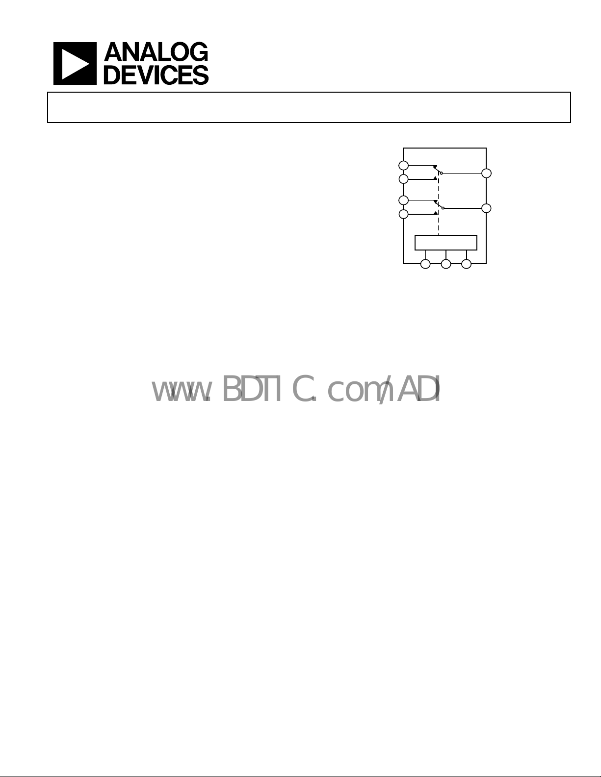
FUNCTIONAL BLOCK DIAGRAM
ADG636
4
S1A
S1B
S2A
S2B
5
11
10
LOGIC
14
1
A0
A1
Figure 1.
EN
6
D1
9
D2
2
02754-001
GENERAL DESCRIPTION
The ADG636 is a monolithic device, comprising two independently selectable CMOS single pole, double throw (SPDT)
switches. When on, each switch conducts equally well in both
directions.
The ADG636 operates from a dual ±2.7 V to ±5.5 V supply, or
from a single supply of +2.7 V to +5.5 V.
This switch offers ultralow charge injection of ±1.5 pC over the
entire signal range and leakage current of 10 pA typical at 25°C.
In addition, it offers on resistance of 85 Ω typical, which is matched
to within 2 Ω between channels. The ADG636 also has low power
dissipation yet is capable of high switching speeds.
The ADG636 exhibits break-before-make switching action and
is available in a 14-lead TSSOP package.
PRODUCT HIGHLIGHTS
1. Ultralow charge injection. Q
full signal range.
2. Leakage current <0.25 nA maximum at 85°C.
3. Dual ±2.7 V to ±5 V or single +2.7 V to +5.5 V supply.
4. Automotive temperature range: −40°C to +125°C.
5. Small 14-lead TSSOP package.
: ±1.5 pC typical over the
INJ
Rev. A
Information furnished by Analog Devices is believed to be accurate and reliable. However, no
responsibility is assumed by Analog Devices for its use, nor for any infringements of patents or other
rights of third parties that may result from its use. Specifications subject to change without notice. No
license is granted by implication or otherwise under any patent or patent rights of Analog Devices.
Trademarks and registered trademarks are the property of their respective owners.
One Technology Way, P.O. Box 9106, Norwood, MA 02062-9106, U.S.A.
Tel: 781.329.4700 www.analog.com
Fax: 781.461.3113 ©2002–2008 Analog Devices, Inc. All rights reserved.
Page 2

ADG636
www.BDTIC.com/ADI
TABLE OF CONTENTS
Features .............................................................................................. 1
Applications ....................................................................................... 1
Functional Block Diagram .............................................................. 1
General Description ......................................................................... 1
Product Highlights ........................................................................... 1
Revision History ............................................................................... 2
Specifications ..................................................................................... 3
Dual Supply ................................................................................... 3
Single Supply ................................................................................. 5
REVISION HISTORY
8/08—Rev. 0 to Rev. A
Updated Format .................................................................. Universal
Changes to Analog Switch Parameter ............................................ 3
Changes to Analog Switch Parameter ............................................ 5
Changes to Analog Switch Parameter ............................................ 7
Change to I
Changes to Absolute Maximum Ratings ....................................... 9
Added Table 5; Renumbered Sequentially .................................. 10
Moved Truth Table ......................................................................... 10
Added Endnote to Table 6 ............................................................. 10
Changes to Figure 19 ...................................................................... 13
Updated Outline Dimensions ....................................................... 16
Changes to Ordering Guide .......................................................... 16
1/02—Revision 0: Initial Version
Parameter .................................................................. 8
DD
Absolute Maximum Ratings ............................................................9
ESD Caution...................................................................................9
Pin Configuration and Function Descriptions ........................... 10
Typical Performance Characteristics ........................................... 11
Test Circuits ..................................................................................... 13
Terminology .................................................................................... 15
Outline Dimensions ....................................................................... 16
Ordering Guide .......................................................................... 16
Rev. A | Page 2 of 16
Page 3
ADG636
www.BDTIC.com/ADI
SPECIFICATIONS
DUAL SUPPLY
VDD = 5 V ± 10%, VSS = −5 V ± 10%, GND = 0 V. All specifications −40°C to +125°C, unless otherwise noted.
Table 1.
Parameter +25°C −40°C to +85°C −40°C to +125°C Unit Test Conditions/Comments
ANALOG SWITCH
Analog Signal Range VSS to VDD V
V
On Resistance, RON 85 Ω typ VS = ±3 V, IDS = −1 mA, Figure 14
115 140 160 Ω max VS = ±3 V, IDS = −1 mA, Figure 14
On-Resistance Match Between
Channels, ΔR
ON
2 Ω typ VS = ±3 V, IDS = −1 mA
4 5.5 6.5 Ω max VS = ±3 V, IDS = −1 mA
On-Resistance Flatness, R
25 Ω typ VS = ±3 V, IDS = −1 mA
FLAT(ON)
40 55 60 Ω max VS = ±3 V, IDS = −1 mA
LEAKAGE CURRENTS VDD = +5.5 V, VSS = −5.5 V
Source Off Leakage, IS (Off) ±0.01 nA typ VS = ±4.5 V, VD = 4.5 V, Figure 15
±0.1 ±0.25 ±2 nA max VS = ±4.5 V, VD = 4.5 V, Figure 15
Drain Off Leakage, ID (Off) ±0.01 nA typ VS = ±4.5 V, VD = 4.5 V, Figure 15
±0.1 ±0.25 ±2 nA max VS = ±4.5 V, VD = 4.5 V, Figure 15
Channel On Leakage, ID (On), IS (On) ±0.01 nA typ VS = VD = ±4.5 V, Figure 16
±0.1 ±0.25 ±6 nA max VS = VD = ±4.5 V, Figure 16
DIGITAL INPUTS
Input High Voltage, V
Input Low Voltage, V
Input Current, I
INL
2.4 V min
INH
0.8 V max
INL
or I
0.005 μA typ VIN = V
INH
±0.1 μA max VIN = V
Digital Input Capacitance, CIN 2 pF typ
DYNAMIC CHARACTERISTICS1
Transition Time 70 ns typ
100 120 150 ns max
tON Enable 100 ns typ
135 170 190 ns max
t
Enable 55 ns typ
OFF
80 90 100 ns max
Break-Before-Make Time Delay, t
20 ns typ
BBM
10 ns min
Charge Injection −1.2 pC typ
Off Isolation −65 dB typ
Channel-to-Channel Crosstalk −65 dB typ
Bandwidth −3 dB 610 MHz typ RL = 50 Ω, CL = 5 pF, Figure 22
= +4.5 V, VSS = −4.5 V
DD
or V
INL
INL
= +3 V, V
V
S1A
= 35 pF, Figure 17
C
L
= +3 V, V
V
S1A
C
= 35 pF, Figure 17
L
= 300 Ω, CL = 35 pF, VS = 3 V,
R
L
Figure 19
= 300 Ω, CL = 35 pF, VS = 3 V,
R
L
Figure 19
= 300 Ω, CL = 35 pF, VS = 3 V,
R
L
Figure 19
= 300 Ω, CL = 35 pF, VS = 3 V,
R
L
Figure 19
= 300 Ω, CL = 35 pF, VS = 3 V,
R
L
Figure 18
= 300 Ω, CL = 35 pF, VS = 3 V,
R
L
Figure 18
= 0 V, RS = 0 Ω, CL = 1 nF,
V
S
Figure 20
= 50 Ω, CL = 5 pF, f = 10 MHz,
R
L
Figure 21
= 50 Ω, CL = 5 pF, f = 10 MHz,
R
L
Figure 23
INH
or V
INH
= −3 V, RL = 300 Ω,
S1B
= −3 V, RL = 300 Ω,
S1B
Rev. A | Page 3 of 16
Page 4
ADG636
www.BDTIC.com/ADI
Parameter +25°C −40°C to +85°C −40°C to +125°C Unit Test Conditions/Comments
CS (Off) 5 pF typ f = 1 MHz
CD (Off) 8 pF typ f = 1 MHz
CD (On), CS (On) 8 pF typ f = 1 MHz
POWER REQUIREMENTS VDD = +5.5 V, VSS = −5.5 V
IDD 0.001 μA typ Digital inputs = 0 V or 5.5 V
1.0 μA max Digital inputs = 0 V or 5.5 V
ISS 0.001 μA typ Digital inputs = 0 V or 5.5 V
1.0 μA max Digital inputs = 0 V or 5.5 V
1
Guaranteed by design; not subject to production test.
Rev. A | Page 4 of 16
Page 5
ADG636
www.BDTIC.com/ADI
SINGLE SUPPLY
VDD = 5 V ± 10%, VSS = 0 V, GND = 0 V. All specifications −40°C to +125°C, unless otherwise noted.
Table 2.
Parameter +25°C −40°C to +85°C −40°C to +125°C Unit Test Conditions/Comments
ANALOG SWITCH
Analog Signal Range 0 V to VDD V
V
On Resistance, RON 210 Ω typ VS = 3.5 V, IDS = −1 mA, Figure 14
290 350 380 Ω max VS = 3.5 V, IDS = −1 mA, Figure 14
On Resistance Match Between Channels, ΔRON 3 Ω typ VS = 3.5 V, IDS = −1 mA
12 13 Ω max VS = 3.5 V, IDS = −1 mA
LEAKAGE CURRENTS VDD = 5.5 V
Source Off Leakage, IS (Off) ±0.01 nA typ
±0.1 ±0.25 ±2 nA max
Drain Off Leakage, ID (Off) ±0.01 nA typ
±0.1 ±0.25 ±2 nA max
Channel On Leakage, ID (On), IS (On) ±0.01 nA typ VS = VD = 4.5 V/1 V, Figure 16
±0.1 ±0.25 ±6 nA max VS = VD = 4.5 V/1 V, Figure 16
DIGITAL INPUTS
Input High Voltage, V
Input Low Voltage, V
Input Current, I
INL
2.4 V min
INH
0.8 V max
INL
or I
0.005 μA typ VIN = V
INH
±0.1 μA max VIN = V
Digital Input Capacitance, CIN 2 pF typ
DYNAMIC CHARACTERISTICS1
Transition Time 90 ns typ
150 185 210 ns max
tON Enable 135 ns typ
180 235 275 ns max
t
Enable 70 ns typ
OFF
105 120 135 ns max
Break-Before-Make Time Delay, t
30 ns typ
BBM
10 ns min
Charge Injection 0.3 pC typ VS = 0 V, RS = 0 Ω, CL = 1 nF,
Figure 20
Off Isolation −60 dB typ
Channel-to-Channel Crosstalk −65 dB typ
Bandwidth −3 dB 530 MHz typ RL = 50 Ω, CL = 5 pF, Figure 22
CS (Off) 5 pF typ f = 1 MHz
CD (Off) 8 pF typ f = 1 MHz
CD (On), CS (On) 8 pF typ f = 1 MHz
= 4.5 V, VSS = 0 V
DD
= 1 V/4.5 V, VD = 4.5 V/1 V,
V
S
Figure 15
V
Figure 15
V
Figure 15
V
Figure 15
V
C
V
C
R
Figure 19
R
Figure 19
R
Figure 19
R
Figure 19
R
Figure 18
R
Figure 18
R
Figure 21
R
Figure 23
= 1 V/4.5 V, VD = 4.5 V/1 V,
S
= 1 V/4.5 V, VD = 4.5 V/1 V,
S
= 1 V/4.5 V, VD = 4.5 V/1 V,
S
or V
INL
INL
= 3 V, V
S1A
= 35 pF, Figure 17
L
= 3 V, V
S1A
= 35 pF, Figure 17
L
= 300 Ω, CL = 35 pF, VS = 3 V,
L
= 300 Ω, CL = 35 pF, VS = 3 V,
L
= 300 Ω, CL = 35 pF, VS = 3 V,
L
= 300 Ω, CL = 35 pF, VS = 3 V,
L
= 300 Ω, CL = 35 pF, VS = 3 V,
L
= 300 Ω, CL = 35 pF, VS = 3 V,
L
= 50 Ω, CL = 5 pF, f = 10 MHz,
L
= 50 Ω, CL = 5 pF, f = 10 MHz,
L
INH
or V
INH
= 0 V, RL = 300 Ω,
S1B
= 0 V, RL = 300 Ω,
S1B
Rev. A | Page 5 of 16
Page 6

ADG636
www.BDTIC.com/ADI
Parameter +25°C −40°C to +85°C −40°C to +125°C Unit Test Conditions/Comments
POWER REQUIREMENTS VDD = 5.5 V
IDD 0.001 μA typ Digital inputs = 0 V or 5.5 V
1.0 μA max Digital inputs = 0 V or 5.5 V
1
Guaranteed by design; not subject to production test.
Rev. A | Page 6 of 16
Page 7

ADG636
www.BDTIC.com/ADI
VDD = 3 V ± 10%, VSS = 0 V, GND = 0 V. All specifications −40°C to +125°C, unless otherwise noted.
Table 3.
Parameter +25°C −40°C to +85°C −40°C to +125°C Unit Test Conditions/Comments
ANALOG SWITCH
Analog Signal Range 0 V to VDD V
V
On Resistance, RON 380 420 460 Ω typ VS = 1.5 V, IDS = −1 mA, Figure 14
On Resistance Match Between Channels, ΔRON 5 Ω typ VS = 1.5 V, IDS = −1 mA
LEAKAGE CURRENTS VDD = 3.3 V
Source Off Leakage, IS (Off) ±0.01 nA typ
±0.1 ±0.25 ±2 nA max
Drain Off Leakage, ID (Off) ±0.01 nA typ
±0.1 ±0.25 ±2 nA max
Channel On Leakage, ID (On), IS (On) ±0.01 nA typ VS = VD = 1 V/3 V, Figure 16
±0.1 ±0.25 ±6 nA max VS = VD = 1 V/3 V, Figure 16
DIGITAL INPUTS
Input High Voltage, V
Input Low Voltage, V
Input Current, I
INL
2.0 V min
INH
0.8 V max
INL
or I
0.005 μA typ VIN = V
INH
±0.1 μA max VIN = V
Digital Input Capacitance, CIN 2 pF typ
DYNAMIC CHARACTERISTICS1
Transition Time 170 ns typ
320 390 450 ns max
tON Enable 250 ns typ
360 460 530 ns max
t
Enable 110 ns typ
OFF
175 205 230 ns max
Break-Before-Make Time Delay, t
80 ns typ
BBM
10 ns min
Charge Injection 0.6 pC typ
Off Isolation −60 dB typ
Channel-to-Channel Crosstalk −65 dB typ
Bandwidth −3 dB 530 MHz typ RL = 50 Ω, CL = 5 pF, Figure 22
CS (Off) 5 pF typ f = 1 MHz
CD (Off) 8 pF typ f = 1 MHz
CD (On), CS (On) 8 pF typ f = 1 MHz
= 2.7 V, VSS = 0 V
DD
= 1 V/3 V, VD = 3 V/1 V,
V
S
Figure 15
V
Figure 15
V
Figure 15
V
Figure 15
V
C
V
C
R
Figure 19
R
Figure 19
R
Figure 19
R
Figure 19
R
Figure 18
R
Figure 18
V
Figure 20
R
Figure 21
R
Figure 23
= 1 V/3 V, VD = 3 V/1 V,
S
= 1 V/3 V, VD = 3 V/1 V,
S
= 1 V/3 V, VD = 3 V/1 V,
S
or V
INL
INL
= 2 V, V
S1A
= 35 pF, Figure 17
L
= 2 V, V
S1A
= 35 pF, Figure 17
L
= 300 Ω, CL = 35 pF, VS = 2 V,
L
= 300 Ω, CL = 35 pF, VS = 2 V,
L
= 300 Ω, CL = 35 pF, VS = 2 V,
L
= 300 Ω, CL = 35 pF, VS = 2 V,
L
= 300 Ω, CL = 35 pF, VS1 = 2 V,
L
= 300 Ω, CL = 35 pF, VS1 = 2 V,
L
= 0 V, RS = 0 Ω, CL = 1 nF,
S
= 50 Ω, CL = 5 pF, f = 10 MHz,
L
= 50 Ω, CL = 5 pF, f = 10 MHz,
L
INH
or V
INH
= 0 V, RL = 300 Ω,
S1B
= 0 V, RL = 300 Ω,
S1B
Rev. A | Page 7 of 16
Page 8

ADG636
www.BDTIC.com/ADI
Parameter +25°C −40°C to +85°C −40°C to +125°C Unit Test Conditions/Comments
POWER REQUIREMENTS VDD = 3.3 V
IDD 0.001 μA typ Digital inputs = 0 V or 3.3 V
1.0 μA max Digital inputs = 0 V or 3.3 V
1
Guaranteed by design; not subject to production test.
Rev. A | Page 8 of 16
Page 9

ADG636
www.BDTIC.com/ADI
ABSOLUTE MAXIMUM RATINGS
TA = 25°C, unless otherwise noted.
Table 4.
Parameter Rating
VDD to VSS 13 V
VDD to GND −0.3 V to +6.5 V
VSS to GND +0.3 V to −6.5 V
Analog Inputs1 V
Digital Inputs1
Peak Current, S or D (Pulsed at 1 ms,
10% Duty Cycle Maximum)
Continuous Current, S or D 10 mA
Operating Temperature Range −40°C to +125°C
Storage Temperature Range −65°C to +150°C
Junction Temperature 150°C
TSSOP Package
θJA Thermal Impedance 150°C/W
θJC Thermal Impedance 27°C/W
Lead Soldering
Lead Temperature, Soldering (10 sec) 300°C
IR Reflow, Peak Temperature (<20 sec) 220°C
Pb-Free Soldering
Reflow, Peak Temperature 260(+0/−5)°C
Time at Peak Temperature 20 sec to 40 sec
1
Overvoltages at EN, A0, A1, S, or D are clamped by internal diodes. Current
should be limited to the maximum ratings given.
− 0.3 V to VDD + 0.3 V
SS
−0.3 V to V
30 mA, whichever
occurs first
20 mA
+ 0.3 V or
DD
Stresses above those listed under Absolute Maximum Ratings
may cause permanent damage to the device. This is a stress
rating only; functional operation of the device at these or any
other conditions above those indicated in the operational
section of this specification is not implied. Exposure to absolute
maximum rating conditions for extended periods may affect
device reliability.
ESD CAUTION
Rev. A | Page 9 of 16
Page 10

ADG636
S
S
www.BDTIC.com/ADI
PIN CONFIGURATION AND FUNCTION DESCRIPTIONS
1
A0
2
EN
3
V
S
S
4
1
A
(Not to Scale)
5
B
1
6
D1
7
NC
NC = NO CONNECT
ADG636
TOP VIEW
14
A1
13
GND
12
V
DD
11
S2A
10
S2B
9
D2
8
NC
02754-002
Figure 2. Pin Configuration
Table 5. Pin Function Descriptions
Pin number Mnemonic Description
1 A0 Digital Input (LSB).
2 EN Active High Digital Input.
3 VSS Negative Power Supply. For single-supply operation, connect this pin to GND.
4 S1A Source Terminal. Can be an input or output.
5 S1B Source Terminal. Can be an input or output.
6 D1 Drain Terminal. Can be an input or output.
7 NC Not Electrically Connected.
8 NC Not Electrically Connected.
9 D2 Drain Terminal. Can be an input or output.
10 S2B Source Terminal. Can be an input or output.
11 S2A Source Terminal. Can be an input or output.
12 VDD Positive Power Supply.
13 GND Ground (0 V) Power Supply.
14 A1 Digital Input (MSB).
Table 6. Truth Table
A1 A0 EN On Switch
1
X
X
1
0 None
0 0 1 S1A, S2A
0 1 1 S1B, S2A
1 0 1 S1A, S2B
1 1 1 S1A, S2B
1
X = logic state doesn’t matter; it can be either 0 or 1.
Rev. A | Page 10 of 16
Page 11

ADG636
www.BDTIC.com/ADI
TYPICAL PERFORMANCE CHARACTERISTICS
250
TA = 25°C
200
VDD,VSS = ±2.5V
150
VDD,VSS = ±3.3V
100
ON RESISTANCE (Ω)
50
VDD,VSS = ±4.5V
VDD,VSS = ±3V
VDD,VSS = ±5V
350
VDD = 5V
= 0V
V
SS
300
250
200
TA = +125°C
150
ON RESISTANCE (Ω)
100
50
TA = +85°C
TA = +25°C
TA = –40°C
0
–5 –4 –3
V
D,VS
(V)
Figure 3. On Resistance vs. VD (VS), Dual Supply
600
TA = 25°C
V
= 0V
SS
500
400
300
200
ON RESISTANCE (Ω)
100
VDD = 2.7V
VDD = 3V
VDD = 4.5V
VDD = 3.3V
0
0
0.5 1.0 1.5 2.0 2.5 3.0 3.5 4.0 4. 5 5.0
V
D
, VS (V)
Figure 4. On Resistance vs. VD (VS), Single Supply
VDD = 5V
5234–2 –1 0 1
02754-003
0
0 0.5 1.0 1.5 2.0 2. 5 3.0 3. 5 4.0 4.5 5.0
V
D,VS
(V)
02754-006
Figure 6. On Resistance vs. VD (VS) for Different Temperatures, Single Supply
5
3
1
–1
–3
–5
–7
CURRENT (nA)
–9
–11
VDD = +5V
–13
V
= –5V
SS
–15
06040 80 100
02754-004
TEMPERATURE (° C)
IS (OFF)
ID (OFF)
ID (ON), IS (ON)
12020
02754-007
Figure 7. Leakage Currents vs. Temperatures, Dual Supply
180
VDD = +5V
V
= –5V
SS
160
140
120
100
80
60
ON RESISTANCE (Ω)
40
20
0
–5 –4 54–3 –2 –1 3210
TA = +125°C
TA = +25°C
TA = +85°C
VD, VS (V)
TA = –40°C
02754-005
Figure 5. On Resistance vs. VD (VS) for Different Temperatures, Dual Supply
Rev. A | Page 11 of 16
5
3
1
–1
–3
–5
–7
CURRENT (nA)
–9
–11
–13
–15
VDD = 5V
V
= 0V
SS
06040 80 100 12020
TEMPERATURE ( °C)
IS (OFF)
ID (OFF)
ID (ON), IS (ON)
Figure 8. Leakage Currents vs. Temperature, Single Supply
02754-008
Page 12

ADG636
A
A
A
A
www.BDTIC.com/ADI
1.0
TA = 25°C
0.5
0
–0.5
–1.0
CHARGE INJECTI ON (pC)
–1.5
–2.0
–5 –4 54–3 –2 –1 3210
Figure 9. Charge Injection vs. Source Voltage
VDD= +3V
V
= 0V
SS
= +5V
V
DD
V
= 0V
SS
= +5V
V
DD
V
= –5V
SS
(V)
V
S
02754-009
0
TA = 25°C
–10
–20
–30
–40
TION (dB)
–50
TTENU
–60
–70
–80
–90
1
FREQUENCY (MHz)
V
= +5V
DD
V
= 0V
SS
VDD= +5V
V
= –5V
SS
1000100100.3
02754-012
Figure 12. Crosstalk vs. Frequency
250
200
150
TIME (ns)
100
50
0
TA = 25 C
VDD= +5V
V
SS
t
ON
–
2
0
Figure 10. tON/t
V
= +5V
DD
V
= 0V
SS
= –5V
t
OFF
V
= +5V
DD
V
= 0V
SS
06040–40 80 100 12020
TEMPERATURE (° C)
Enable Timing vs. Temperature
OFF
VDD= +5V
V
= –5V
SS
02754-010
0
TA = 25 C
–2
–4
–6
–8
TION (dB)
–10
TTENU
–12
–14
–16
–18
FREQUENCY (MHz)
VDD= +5V
V
= –5V
SS
= +5V
V
DD
V
= 0V
SS
1000100100.3 1
02754-013
Figure 13. On Response vs. Frequency
0
TA = 25 C
–10
–20
= +5V
V
–30
–40
–50
–60
AT T E NUAT IO N ( d B)
–70
–80
–90
DD
V
= 0V
SS
FREQUENCY (MHz)
VDD= +5V
V
= –5V
SS
1000100100.3 1
02754-011
Figure 11. Off Isolation vs. Frequency
Rev. A | Page 12 of 16
Page 13

ADG636
V
V
V
V
V
V
V
V
www.BDTIC.com/ADI
TEST CIRCUITS
I
DS
V1
IS(OFF) ID(OFF)
SD
S
RON = V1/I
DS
02754-014
V
S
SD
A
A
V
D
02754-015
NC
SD
NC = NO CONNECT
Figure 14. On Resistance Figure 15. Off Leakage Figure 16. On Leakage
DD
0.1µF 0.1µF
A1
V
S
2.4V
50Ω
A0
EN
SS
V
OUT
3V
)
IN
0V
V
OUT
TRANSITION
50%
t
TRANSITION
90%
50%
t
TRANSITION
90%
02754-017
S1A
S1B
ADDRESS
DRIVE (V
C
L
35pF
V
V
SS
DD
S1A
S1B
D1
GND
R
L
300Ω
V
V
Figure 17. Transition Time, t
DD
0.1µF 0. 1µF
A0
A1
2.4V
50Ω
EN
S
SS
V
V
SS
DD
S1A
S1B
D1
GND
R
L
300Ω
V
S
Figure 18. Break-Before-Make Delay, t
C
L
35pF
ADDRESS
DRIVE (V
V
OUT
3V
)
IN
0V
V
OUT
80%
BBM
t
BBM
80%
2754-018
DD
0.1µF 0.1µF
A0
A1
EN
V
50Ω
S
SS
IN
OUTPUT
(EN), t
ON
3V
)
0V
V
OUT
0V
(EN)
OFF
50%
90%
t
(EN)
ON
50%
90%
t
(EN)
OFF
02754-019
C
L
35pF
ENABLE
DRIVE (V
V
OUT
V
V
SS
DD
S1A
S1B
D1
GND
R
L
300Ω
V
S
Figure 19. Enable Delay, t
ID(ON)
A
V
D
02754-016
Rev. A | Page 13 of 16
Page 14

ADG636
V
V
V
V
V
V
VDDV
www.BDTIC.com/ADI
DD
SS
V
V
DD
SS
R
S
V
S
SD
DECODER
GND
A2A1
EN
C
1nF
V
OUT
L
V
OUT
V
IN
SW OFF SW OFF
SW OFF
V
IN
CHARGE INJECTI ON = ΔV
Q
INJ
OUT
= CL × ΔV
SW ON
SW ON
×C
L
OUT
ΔV
OUT
SW OFF
02754-020
Figure 20. Charge Injection
DD
0.1µF 0.1µF
V
OFF ISOLATION = 20 log
SS
NETWORK
V
DD
SS
S
D
GND
50Ω
V
OUT
V
S
ANALYZER
50Ω
V
V
OUT
R
L
50Ω
S
02754-021
Figure 21. Off Isolation
DD
0.1µF 0.1µF
SS
V
V
DD
SS
S
D
GND
INSERTION LOSS = 20 log
WITH SWITCH
V
OUT
V
WITHOUT SWITCH
OUT
NETWORK
ANALYZER
50Ω
V
V
OUT
R
L
50Ω
S
02754-022
Figure 22. Bandwidth
0.1µF 0. 1µF
NETWORK
ANALYZER
V
OUT
CHANNEL-TO-CHANNEL CROSSTAL K = 20 log
50Ω
V
R
L
50Ω
S
V
S1
S2
SS
V
DD
SS
D
R
L
50Ω
GND
V
OUT
V
S
02754-023
Figure 23. Channel-to-Channel Crosstalk
Rev. A | Page 14 of 16
Page 15

ADG636
www.BDTIC.com/ADI
TERMINOLOGY
I
VDD
Most positive supply potential.
V
SS
Most negative power supply in a dual-supply application.
In single-supply applications, this should be tied to ground at
the device.
GND
Ground (0 V) reference.
I
DD
Positive supply current.
I
SS
Negative supply current.
S
Source terminal. May be an input or output.
D
Drain terminal. May be an input or output.
R
ON
Ohmic resistance between Terminal D and Terminal S.
ΔR
ON
On resistance match between any two channels (that is,
R
max − RON min).
ON
R
FLAT(ON)
Flatness is defined as the difference between the maximum and
minimum values of on resistance as measured over the specified
analog signal range.
I
(Off)
S
Source leakage current with the switch off.
I
(Off)
D
Drain leakage current with the switch off.
I
(On), IS (On)
D
Channel leakage current with the switch on.
V
, VS
D
Analog voltage on Terminal D and Terminal S.
V
INL
Maximum input voltage for Logic 0.
V
INH
Minimum input voltage for Logic 1.
INL(IINH)
Input current of the digital input.
C
(Off)
S
Channel input capacitance for the off condition.
C
(Off)
D
Channel output capacitance for the off condition.
C
(On), CS (On)
D
On switch capacitance.
C
IN
Digital input capacitance.
t
(EN)
ON
Delay time between the 50% and 90% points of the digital input
and the switch on condition.
t
(EN)
OFF
Delay time between the 50% and 90% points of the digital input
and the switch off condition.
t
TRANSITION
Delay time between the 50% and 90% points of the digital input
and the switch on condition when switching from one address
state to another.
t
BBM
Off time or on time measured between the 80% points of both
switches when switching from one address state to another.
Charge Injection
A measure of the glitch impulse transferred from the digital
input to the analog output during switching.
Crosstalk
A measure of unwanted signal that is coupled through from one
channel to another as a result of parasitic capacitance.
Off Isolation
A measure of unwanted signal coupling through an off switch.
Bandwidth
The frequency response of the on switch.
Insertion Loss
Loss due to the on resistance of the switch.
Rev. A | Page 15 of 16
Page 16

ADG636
www.BDTIC.com/ADI
OUTLINE DIMENSIONS
5.10 (0.201)
5.00 (0.197)
4.90 (0.193)
4.50 (0.177)
4.40 (0.173)
4.30 (0.169)
PIN 1
1.05 (0.041)
1.00 (0.039)
0.80 (0.031)
0.15 (0.006)
0.05 (0.002)
COPLANARITY
0.10 (0.004)
14
1
0.65 (0.025)
BSC
0.30 (0.012)
0.19 (0.007)
CONTROLLING DIMENSIONSARE IN MILLIMETERS; INCH DIMENSIONS
(IN PARENTHESES) ARE ROUNDED-O FF MIL LIMETE R EQUIVALENTS FOR
REFERENCE ON LY AND ARE NOT APPROPRI ATE FOR USE IN DESIGN.
8
6.40 (0.252)
BSC
7
1.20 (0.047)
MAX
0.20 (0.008)
0.09 (0.003)
SEATING
PLANE
COMPLIANT TO JEDEC ST ANDARDS MO-153-AB-1
8°
0°
0.75 (0.029)
0.60 (0.023)
0.45 (0.018)
061908-A
Figure 24. 14-Lead Thin Shrink Small Outline Package [TSSOP]
(RU-14)
Dimensions shown in millimeters and (inches)
ORDERING GUIDE
Model Temperature Range Package Description Package Option
ADG636YRU −40°C to +125°C 14-Lead Thin Shrink Small Outline Package [TSSOP] RU-14
ADG636YRU-REEL −40°C to +125°C 14-Lead Thin Shrink Small Outline Package [TSSOP] RU-14
ADG636YRUZ1 −40°C to +125°C 14-Lead Thin Shrink Small Outline Package [TSSOP] RU-14
ADG636YRUZ-REEL1 −40°C to +125°C 14-Lead Thin Shrink Small Outline Package [TSSOP] RU-14
ADG636YRUZ-REEL 7
1
Z = RoHS Compliant Part.
1
−40°C to +125°C 14-Lead Thin Shrink Small Outline Package [TSSOP] RU-14
©2002–2008 Analog Devices, Inc. All rights reserved. Trademarks and
registered trademarks are the property of their respective owners.
D02754-0-8/08(A)
Rev. A | Page 16 of 16
 Loading...