

Page 1
CMOS ±5 V/+5 V,
R
R
www.BDTIC.com/ADI
FEATURES
5.5 Ω (maximum) on resistance
0.9 Ω (maximum) on resistance flatness
2.7 V to 5.5 V single supply
±2.7 V to ±5.5 V dual supply
Rail-to-rail operation
10-lead MSOP package
Typical power consumption (<0.01 μW)
TTL-/CMOS-compatible inputs
APPLICATIONS
Automatic test equipment
Power routing
Communication systems
Data acquisition systems
Sample-and-hold systems
Avio nics
Relay replacements
Battery-powered systems
GENERAL DESCRIPTION
The ADG621/ADG622/ADG623 are monolithic, CMOS,
single-pole, single-throw (SPST) switches. Each switch of the
ADG621/ADG622/ADG623 conducts equally well in both
directions when on.
The ADG621/ADG622/ADG623 contain two independent
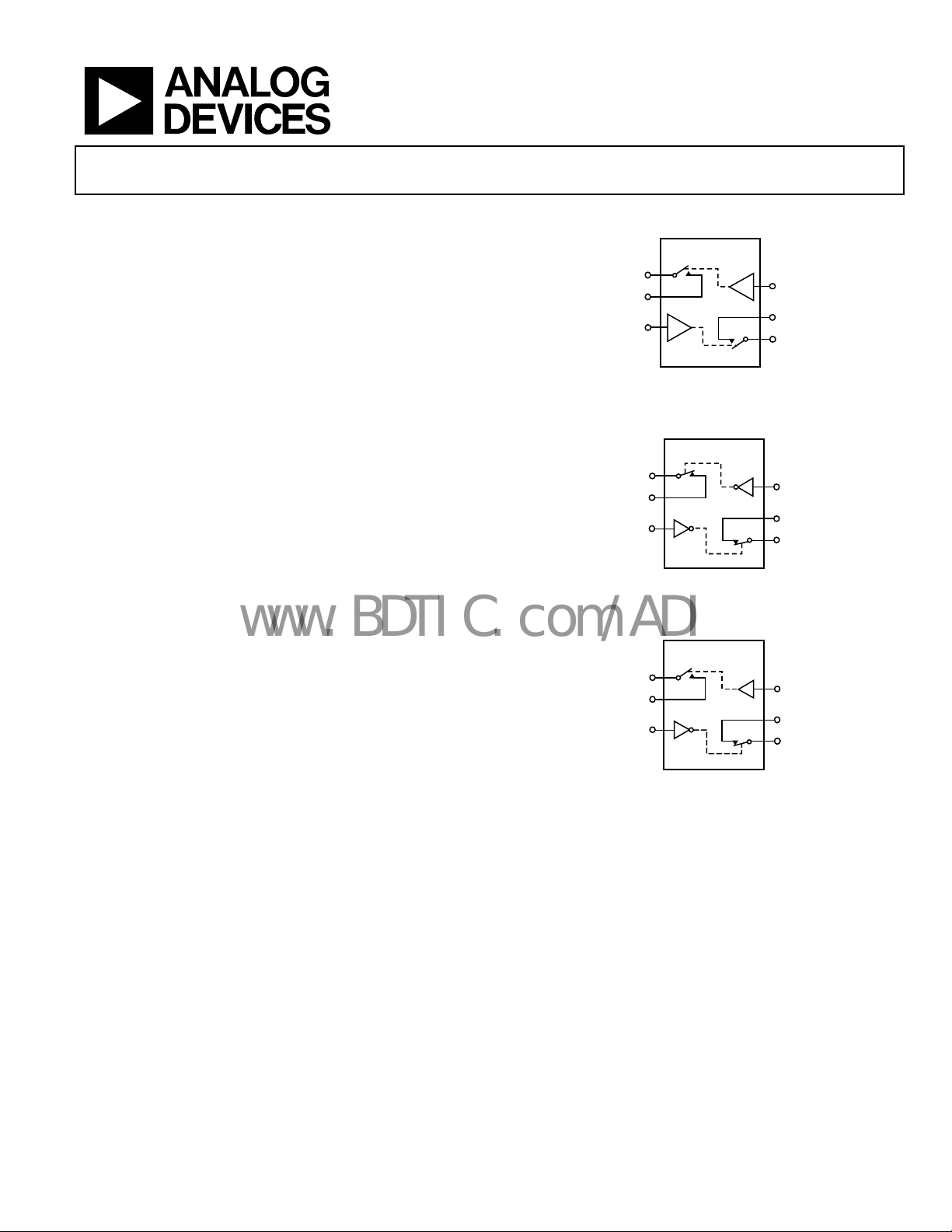
switches. The ADG621 and ADG622 differ only in that both
switches are normally open and normally closed. In the ADG623,
Switch 1 is normally open, and Switch 2 is normally closed. The
ADG623 exhibits break-before-make switching action.
The ADG621/ADG622/ADG623 offer low on resistance of
4 Ω, which is matched to within 0.25 Ω between channels.
These switches also provide low power dissipation yet give
high switching speeds. The ADG621/ADG622/ADG623 are
available in a 10-lead MSOP package.
4 Ω Dual SPST Switches
ADG621/ADG622/ADG623
FUNCTIONAL BLOCK DIAGRAMS
ADG621
S1
D1
IN2
NOTES
1. SWITCHES SHOWN FO
Figure 1.
ADG622
S1
D1
IN2
NOTES
1. SWITCHES SHOWN FOR A LOGIC 0 INPUT
Figure 2.
ADG623
S1
D1
IN2
NOTES
1. SWITCHES SHOWN FO
Figure 3.
PRODUCT HIGHLIGHTS
1. Low on resistance, R
2. Dual ±2.7 V to ±5.5 V or single +2.7 V to +5.5 V.
3. Low power dissipation; CMOS construction ensures low
power dissipation.
4. Tiny 10-lead MSOP package.
(4 Ω typical).
ON
IN1
D2
S2
A LOGIC 0 INPUT
IN1
D2
S2
IN1
D2
S2
A LOGIC 0 INPUT
02616-001
02616-002
02616-003
Rev. A
Information furnished by Analog Devices is believed to be accurate and reliable. However, no
responsibility is assumed by Anal og Devices for its use, nor for any infringements of patents or ot her
rights of third parties that may result from its use. Specifications subject to change without notice. No
license is granted by implication or otherwise under any patent or patent rights of Analog Devices.
Trademarks and registered trademarks are the property of their respective owners.
One Technology Way, P.O. Box 9106, Norwood, MA 02062-9106, U.S.A.
Tel: 781.329.4700 www.analog.com
Fax: 781.461.3113 ©2001–2007 Analog Devices, Inc. All rights reserved.
Page 2

ADG621/ADG622/ADG623
www.BDTIC.com/ADI
TABLE OF CONTENTS
Features.............................................................................................. 1
Applications....................................................................................... 1
General Description ......................................................................... 1
Functional Block Diagrams............................................................. 1
Product Highlights ........................................................................... 1
Revision History ............................................................................... 2
Specifications..................................................................................... 3
Dual Supply................................................................................... 3
Single Supply................................................................................. 4
REVISION HISTORY
6/07—Rev. 0 to Rev. A
Change to On Resistance Flatness, R
Specification (Table 1)...................................................................... 3
Change to On Resistance Flatness, R
Specification (Table 2)...................................................................... 4
Added Table 6.................................................................................... 6
Changes to Terminology Section.................................................... 7
Changes to Figure 13........................................................................ 9
Updated Outline Dimensions....................................................... 12
Changes to Ordering Guide.......................................................... 12
11/01—Revision 0: Initial Version
FLAT(ON)
FLAT(ON)
Absolute Maximum Ratings ............................................................5
ESD Caution...................................................................................5
Pin Configuration and Function Descriptions..............................6
Terminology.......................................................................................7
Typical Performance Characteristics..............................................8
Test Circuits..................................................................................... 10
Outline Dimensions....................................................................... 12
Ordering Guide .......................................................................... 12
Rev. A | Page 2 of 12
Page 3
ADG621/ADG622/ADG623
www.BDTIC.com/ADI
SPECIFICATIONS
DUAL SUPPLY1
VDD = +5 V ± 10%, VSS = −5 V ± 10%, GND = 0 V, unless otherwise noted.
Table 1.
Parameter +25°C −40°C to +85°C Unit Test Conditions/Comments
ANALOG SWITCH
Analog Signal Range VSS to VDD V VDD = +4.5 V, VSS = −4.5 V
On Resistance, RON 4 Ω typ
5.5 7 Ω max
On Resistance Match Between Channels, ∆RON 0.25 Ω typ VS = ±4.5 V, IS = −10 mA
0.35 0.4 Ω max
On Resistance Flatness, R
0.9 0.9 Ω typ VS = ±3.3 V, IS = −10 mA
FLAT(ON)
1.5 Ω max
LEAKAGE CURRENTS VDD = +5.5 V, VSS = −5.5 V
Source Off Leakage, IS (Off) ±0.01 nA typ
±0.25 ±1 nA max
Drain Off Leakage, ID (Off) ±0.01 nA typ
±0.25 ±1 nA max
Channel On Leakage, ID, IS (On) ±0.01 nA typ
±0.25 ±1 nA max
DIGITAL INPUTS
Input High Voltage, V
Input Low Voltage, V
Input Current, I
2.4 V min
INH
0.8 V max
INL
or I
0.005 μA typ VIN = V
INL
INH
±0.1 μA max
Digital Input Capacitance, CIN 2 pF typ
DYNAMIC CHARACTERISTICS2
tON 75 ns typ
120 155 ns max
t
45 ns typ
OFF
70 85 ns max
Break-Before-Make Time Delay, t
(ADG623 Only) 30 ns typ RL = 300 Ω, CL = 35 pF; V
BBM
10 ns min
Charge Injection 110 pC typ
Off Isolation −65 dB typ
Channel-to-Channel Crosstalk −90 dB typ
Bandwidth −3 dB 230 MHz typ
CS (Off) 20 pF typ f = 1 MHz
CD (Off) 20 pF typ f = 1 MHz
CD, CS (On) 70 pF typ f = 1 MHz
POWER REQUIREMENTS VDD = 5.5 V, VSS = –5.5 V
IDD 0.001 μA typ Digital inputs = 0 V or 5.5 V
1.0 μA max
ISS 0.001 μA typ Digital inputs = 0 V or 5.5 V
1.0 μA max
1
Temperature range is as follows: B version, –40°C to +85°C.
2
Guaranteed by design; not subject to production test.
V
= ±4.5 V, IS = −10 mA, see Figure 16
S
V
= ±4.5 V, VD = m 4.5 V, see Figure 17
S
V
= ±4.5 V, VD = m 4.5 V, see Figure 17
S
V
= VD = ±4.5 V, see Figure 18
S
or V
INL
R
= 300 Ω, CL = 35 pF; VS = 3.3 V, see Figure 19
L
R
= 300 Ω, CL = 35 pF; VS = 3.3 V, see Figure 19
L
See
Figure 20
V
= 0 V, RS = 0 Ω, CL = 1 nF, see Figure 21
S
R
= 50 Ω, CL = 5 pF, f = 1 MHz, see Figure 22
L
R
= 50 Ω, CL = 5 pF, f = 1 MHz, see Figure 23
L
R
= 50 Ω, CL = 5 pF, see Figure 24
L
INH
= VS2 = 3.3 V
S1
Rev. A | Page 3 of 12
Page 4
ADG621/ADG622/ADG623
www.BDTIC.com/ADI
SINGLE SUPPLY1
VDD = 5 V ± 10%, VSS = 0 V, GND = 0 V, unless otherwise noted.
Table 2.
Parameter +25°C –40°C to +85°C Unit Test Conditions/Comments
ANALOG SWITCH
Analog Signal Range 0 to VDD V VDD = 4.5 V, VSS = 0 V
On Resistance, RON 7 Ω typ
10 12.5 Ω max
On Resistance Match Between Channels, ∆RON 0.5 Ω typ VS = 0 V to 4.5 V, IS = −10 mA
0.75 1 Ω max
On Resistance Flatness, R
0.5 0.5 Ω typ VS = 1.5 V to 3.3 V, IS = −10 mA
FLAT(ON)
1.2 Ω max
LEAKAGE CURRENTS VDD = 5.5 V
Source Off Leakage IS (Off) ±0.01 nA typ
±0.25 ±1 nA max
Drain Off Leakage ID (Off) ±0.01 nA typ
±0.25 ±1 nA max
Channel On Leakage, ID, IS (On) ±0.01 nA typ
±0.25 ±1 nA max
DIGITAL INPUTS
Input High Voltage, V
Input Low Voltage, V
Input Current, I
2.4 V min
INH
0.8 V max
INL
or I
0.005 μA typ VIN = V
INL
INH
±0.1 μA max
Digital Input Capacitance, CIN 2 pF typ
DYNAMIC CHARACTERISTICS2
tON 120 ns typ
210 260 ns max
t
50 ns typ
OFF
75 100 ns max
Break-Before-Make Time Delay, t
(ADG623 Only) 70 ns typ RL = 300 Ω, CL = 35 pF, VS1 = VS2 = 3.3 V
BBM
10 ns min
Charge Injection 6 pC typ
Off Isolation –65 dB typ
Channel-to-Channel Crosstalk –90 dB typ
Bandwidth −3 dB 230 MHz typ
CS (Off) 20 pF typ f = 1 MHz
CD (Off) 20 pF typ f = 1 MHz
CD, CS (On) 70 pF typ f = 1 MHz
POWER REQUIREMENTS VDD = 5.5 V
IDD 0.001 μA typ Digital Inputs = 0 V or 5.5 V
1.0 μA max
1
Temperature range is as follows: B Version, –40°C to +85°C.
2
Guaranteed by design; not subject to production test.
V
= 0 V to 4.5 V, IS = –10 mA, see Figure 16
S
V
= 1 V/4.5 V, VD = 4.5 V/1 V, see Figure 17
S
V
= 1 V/4.5 V, VD = 4.5 V/1 V, see Figure 17
S
V
= VD = 1 V/4.5 V, see Figure 18
S
or V
INL
R
= 300 Ω, CL = 35 pF; VS = 3.3 V, see Figure 19
L
R
= 300 Ω, CL = 35 pF; VS = 3.3 V, see Figure 19
L
See
Figure 20
V
= 0 V; RS = 0 Ω, CL = 1 nF, see Figure 21
S
R
= 50 Ω, CL = 5 pF, f = 1 MHz, see Figure 22
L
R
= 50 Ω, CL = 5 pF, f = 1 MHz, see Figure 23
L
R
= 50 Ω, CL = 5 pF, see Figure 24
L
INH
Rev. A | Page 4 of 12
Page 5

ADG621/ADG622/ADG623
www.BDTIC.com/ADI
ABSOLUTE MAXIMUM RATINGS
TA = 25°C, unless otherwise noted.
Table 3.
Parameter Rating
VDD to V
VDD to GND −0.3 V to +6.5 V
VSS to GND +0.3 V to –6.5 V
Analog Inputs
Digital Inputs
Peak Current, S or D
Continuous Current, S or D 50 mA
Operating Temperature Range
Storage Temperature Range –65°C to +150°C
Junction Temperature 150°C
MSOP Package
Lead Soldering
Pb-Free Soldering
1
Overvoltages at INx, S, or D must be clamped by internal diodes. Currents
should be limited to the maximum ratings given.
13 V
SS
1
1
Industrial (B Version) –40°C to +85°C
θJA Thermal Impedance 206°C/W
θJC Thermal Impedance 44°C/W
Lead Temperature, Soldering
(10 sec)
IR Reflow, Peak Temperature 220°C
Reflow, Peak Temperature 260(+0/−5)°C
Time at Peak Temperature 20 sec to 40 sec
VSS – 0.3 V to VDD + 0.3 V
–0.3 V to VDD + 0.3 V or 30 mA,
whichever occurs first
100 mA (pulsed at 1 ms,
10% duty c
300°C
ycle maximum)
Stresses above those listed under Absolute Maximum Ratings
ma
y cause permanent damage to the device. This is a stress
rating only; functional operation of the device at these or any
other conditions above those listed in the operational sections
of this specification is not implied. Exposure to absolute
maximum rating conditions for extended periods may affect
device reliability.
Only one absolute maximum rating may be applied at any
time.
one
Table 4. ADG621/ADG622 Truth Table
ADG621 INx ADG622 INx Switch Sx Condition
0 1 Off
1 0 On
Table 5. ADG623 Truth Table
INx Switch S1 Switch S2
0 Off On
1 On Off
ESD CAUTION
Rev. A | Page 5 of 12
Page 6

ADG621/ADG622/ADG623
www.BDTIC.com/ADI
PIN CONFIGURATION AND FUNCTION DESCRIPTIONS
1
S1
ADG621/
2
D1
ADG622/
3
IN2
ADG623
4
GND
V
TOP VIEW
(Not to Scale)
5
SS
NC = NO CONNECT
Figure 4. 10-Lead MSOP (RM-10)
Table 6. Pin Function Descriptions
Pin No. Mnemonic Description
1, 7 S1, S2 Source Terminal. May be an input or an output.
2, 8 D1, D2 Drain Terminal. May be an input or an output.
3, 9 IN2, IN1 Control Input.
4 GND Ground (0 V) Reference.
5 VSS
Most Negative Power Supply in a Dual-Supply Applica
ground at the device.
6 NC No Connect.
10 VDD Most Positive Power Supply Potential.
10
V
DD
9
IN1
8
D2
7
S2
NC
6
02616-004
tion. In single-supply applications, this should be tied to
Rev. A | Page 6 of 12
Page 7

ADG621/ADG622/ADG623
www.BDTIC.com/ADI
TERMINOLOGY
IDD
Positive supply current.
I
SS
Negative supply current
(VS)
V
D
Analog voltage on Terminal D and Terminal S.
R
ON
Ohmic resistance between Terminal D and Terminal S.
R
FLAT (ON)
On resistance flatness is defined as the difference between the
maximum and minimum value of on resistance as measured
over the specified analog signal range.
ΔR
ON
On resistance match between any two channels.
I
(Off)
S
Source leakage current with the switch off.
I
(Off)
D
Drain leakage current with the switch off.
I
, IS (On)
D
Channel leakage current with the switch on.
V
INL
Maximum input voltage for Logic 0.
V
INH
Minimum input voltage for Logic 1.
I
(I
)
INL
INH
Input current of the digital input.
C
(Off)
S
Off switch source capacitance. Measured with reference to
ground.
(Off)
C
D
Off switch drain capacitance. Measured with reference to
ground.
C
, CS (On)
D
On switch capacitance. Measured with reference to ground.
C
IN
Digital input capacitance.
t
ON
Delay time between the 50% and the 90% points of the digital
input and switch on condition.
t
OFF
Delay time between the 50% and the 90% points of the digital
input and switch off condition.
t
BBM
On or off time measured between the 90% points of both
switches when switching from one address state to another.
Charge Injection
A measure of the glitch impulse transferred from the digital
input to the analog output during on-off switching.
Off Isolation
A measure of an unwanted signal coupling through an
off switch.
Crosstalk
A measure of an unwanted signal that is coupled through from
one channel to another as a result of parasitic capacitance.
−3 dB Bandwidth
The frequency at which the output is attenuated by 3 dB.
On Response
The frequency response of the on switch.
Insertion Loss
The attenuation between the input and output ports of the
switch when the switch is in the on condition and is due to
the on resistance of the switch.
Rev. A | Page 7 of 12
Page 8

ADG621/ADG622/ADG623
www.BDTIC.com/ADI
TYPICAL PERFORMANCE CHARACTERISTICS
8
TA = 25°C
7
6
5
V
4
, VSS = ±4.5V
V
DD
3
ON RESISTANCE (Ω)
2
1
0
–5 –4 –3 –2 –1 0 1 2 3 54
DD
Figure 5. On Resistance vs. V
20
16
12
VDD = 3.3V
8
ON RESIST ANCE (Ω)
4
0
VDD = 5V
123405
Figure 6. On Resistance vs. V
VDD, VSS = ±2.5V
V
DD
, VSS = ±3.3V
V
D
VDD = 2.7V
VDD = 3V
V
D
, VSS = ±3V
V
DD
, VS (V)
, VS (Dual Supply)
D
, VS (V)
, VS (Single Supply)
D
, VSS = ±5V
TA = 25°C
V
SS
VDD = 4.5V
= 0V
10
9
8
7
6
5
4
ON RESISTANCE (Ω)
3
2
1
02616-005
0
01234
Figure 8. On Resistance vs. V
T
= +85°C
A
T
= +25°C
A
TA = –40°C
VD, VS (V)
, VS for Different Temperature
D
VDD = 5V
= 0V
V
SS
02616-008
5
(Single Supply)
0.5
0.4
0.3
0.2
0.1
0
–0.1
–0.2
LEAKAGE CURRENT (nA)
VDD = +5V
–0.3
V
SS
=±4.5V
V
–0.4
D
= ±4.5V
V
02616-006
S
–0.5
0 1020304050
ID, IS (ON)
= 0V
TEMPERATURE (°C)
IS (OFF)
ID (OFF)
60
70 80
02616-009
Figure 9. Leakage Current vs. Temperature (Dual Supply)
6
5
4
3
2
ON RESISTANCE (Ω)
1
0
–5
–3 –1 1 53–4 –2 0 2 4
Figure 7. On Resistance vs. V
TA = +85°C
TA = +25°C
TA = –40°C
VD, VS (V)
, VS for Different Temperatures
D
VDD = +5V
=–5V
V
SS
02616-007
(Dual Supply)
Rev. A | Page 8 of 12
0.5
0.4
0.3
0.2
0.1
0
–0.1
–0.2
LEAKAGE CURRENT (nA)
–0.3
–0.4
–0.5
ID, IS (ON)
VDD = 5V
= 0V
V
SS
= 4.5V/1V
V
D
= 1V/4.5V
V
S
0 1020304050
TEMPERATURE (°C)
IS (OFF)
ID (OFF)
60
70 80
Figure 10. Leakage Current vs. Temperature (Single Supply)
02616-010
Page 9

ADG621/ADG622/ADG623
A
A
A
A
A
A
www.BDTIC.com/ADI
250
TA = 25°C
200
= +5V
V
DD
V
=–5V
150
100
CHARGE INJECTI ON (pC)
50
0
–5
–4 –3 –2 –1 0 1 2 3 5
SS
VDD = +5V
V
= 0V
SS
V
S
Figure 11. Charge Injection vs. Source Voltage
180
160
140
120
100
80
TIME (ns)
60
40
20
0
–40 –20 0 20 40 60 80
Figure 12. t
t
ON
t
OFF
VDD = +5V
V
= 0V
SS
ON/tOFF
VDD = +5V
= 0V
V
SS
TEMPERATURE (° C)
Times vs. Temperature
VDD = +5V
=–5V
V
SS
VDD = +5V
=–5V
V
SS
0
VDD = +5V
= –5V
V
SS
–10
= 25°C
T
A
–20
–30
–40
TION (dB)
–50
TTENU
–60
–70
–80
02616-011
4
–90
0.2 1 10 100
FREQUE NCY (MHz)
02616-014
Figure 14. Cross talk vs. Frequency
0
VDD = +5V
–2
= –5V
V
SS
= 25°C
T
A
–4
–6
TION (dB)
–8
TTENU
–10
–12
02616-012
–14
0.2 1k10
1 100
FREQUENCY ( MHz)
02616-015
Figure 15. On Response vs. Frequency
0
–10
–20
–30
–40
TION (dB)
–50
TTENU
–60
–70
–80
–90
0.2 1 10 100
FREQUE NCY (MHz)
VDD = +5V
V
T
= –5V
SS
= 25°C
A
02616-013
Figure 13. Off Isolation vs. Frequency
Rev. A | Page 9 of 12
Page 10

ADG621/ADG622/ADG623
V
V
V
V
V
www.BDTIC.com/ADI
TEST CIRCUITS
I
DS
V1
IS(OFF) ID(OFF)
SD
V
S
RON = V1/I
DS
02616-016
S
SD
A
A
V
D
02616-017
NC
SD
NC = NO CONNECT
Figure 16. On Resistance Figure 17. Off Leakage Figure 18. On Leakage
V
SS
DD
0.1µF
0.1µF
ID(ON)
A
V
D
02616-018
V
V
DD
SS
V
C
L
35pF
OUT
SD
R
V
S
IN
GND
L
300Ω
Figure 19. Switching Times (t
ADG621
V
IN
V
IN
ADG622
V
OUT
, t
ON
OFF
50% 50%
50% 50%
t
ON
)
90% 90%
t
OFF
02616-019
0.1µF
V
DD
S1
V
S1
S2
V
S2
IN1, IN2
V
IN
GND
0.1µF
V
V
SS
D1
V
R
OUT2
D2
R
C
L2
300Ω
35pF
L1
300Ω
L2
C
L1
35pF
V
OUT1
Figure 20. Break-Before-Make Time Delay, t
IN
0V
V
OUT1
0V
V
OUT2
0V
(ADG623 Only)
BBM
50% 50%
90%
90%
t
BBM
90%
90%
t
BBM
02616-020
SS
DD
V
DD
SS
V
V
DD
SS
R
S
V
S
SD
IN
GND
C
1nF
V
OUT
L
SW ON
V
IN
V
OUT
Q
INJ
SW OFF
= C
L
× ΔV
OUT
ΔV
OUT
Figure 21. Charge Injection
Rev. A | Page 10 of 12
02616-021
Page 11

ADG621/ADG622/ADG623
VDDV
VDDV
VDDV
www.BDTIC.com/ADI
0.1µF
V
IN
V
IN
OFF ISOLATION = 20 LOG
SS
0.1µF
NETWORK
V
DD
SS
S
D
GND
50Ω
V
OUT
V
S
ANALYZER
50Ω
V
V
OUT
R
L
50Ω
S
02616-022
Figure 22. Off Isolation
SS
0.1µF
V
DD
SS
D1
S2
GND
S1
D2
R
50Ω
R
50Ω
NETWORK
ANALYZER
V
OUT
50Ω
V
R
50Ω
S
0.1µF
V
L
IN
V
CHANNEL-TO -CHANNEL CROSSTALK = 20 LOG
OUT
V
S
02616-023
Figure 23. Channel-to-Channel Crosstalk
0.1µF
V
IN
V
IN
INSERTION LOSS = 20 LOG
SS
0.1µF
NETWORK
V
DD
SS
S
D
GND
V
OUT
V
WITHOUT SWITCH
OUT
ANALYZER
50Ω
R
L
50Ω
WITH SWITCH
V
S
V
OUT
02616-024
Figure 24. Bandwidth
Rev. A | Page 11 of 12
Page 12

ADG621/ADG622/ADG623
www.BDTIC.com/ADI
OUTLINE DIMENSIONS
3.10
3.00
2.90
6
10
3.10
3.00
2.90
1
PIN 1
0.50 BSC
0.95
0.85
0.75
0.15
0.05
0.33
0.17
COPLANARITY
0.10
COMPLIANT TO JEDEC STANDARDS MO-187-BA
Figure 25. 10-Lead Mini Small Outline Package [MSOP]
ORDERING GUIDE
Model Temperature Range Package Description Package Option Branding
ADG621BRM –40°C to +85°C 10-Lead Mini Small Outline Package [MSOP] RM-10 SXB
ADG621BRM-REEL –40°C to +85°C 10-Lead Mini Small Outline Package [MSOP] RM-10 SXB
ADG621BRM–REEL7 –40°C to +85°C 10-Lead Mini Small Outline Package [MSOP] RM-10
ADG621BRMZ
ADG621BRMZ-REEL
ADG622BRM –40°C to +85°C 10-Lead Mini Small Outline Package [MSOP] RM-10 SYB
ADG622BRM-REEL –40°C to +85°C 10-Lead Mini Small Outline Package [MSOP] RM-10 SYB
ADG622BRM-REEL7 –40°C to +85°C 10-Lead Mini S
ADG622BRMZ
ADG622BRMZ-REEL
ADG622BRMZ-REEL7
ADG623BRM –40°C to +85°C 10-Lead Mini Small Outline Package [MSOP] RM-10 SZB
ADG623BRM-REEL –40°C to +85°C 10-Lead Mini Small Outline Package [MSOP] RM-10 SZB
ADG623BRM-REEL7 –40°C to +85°C 10-Lead Mini S
ADG623BRMZ
ADG623BRMZ-REEL
ADG623BRMZ-REEL7
1
Z= RoHS Compliant Part, # denotes RoHS compliant product and may be top or bottom marked.
1
1
1
–40°C to +85°C 10-Lead Mini Small Outline Package [MSOP] RM-10 SXB#
1
–40°C to +85°C 10-Lead Mini Small Outline Package [MSOP] RM-10 SXB#
–40°C to +85°C 10-Lead Mini Small Outline Package [MSOP] RM-10 S12
1
–40°C to +85°C 10-Lead Mini Small Outline Package [MSOP] RM-10 S12
1
–40°C to +85°C 10-Lead Mini Small Outline Package [MSOP] RM-10 S12
–40°C to +85°C 10-Lead Mini Small Outline Package [MSOP] RM-10 S1F
1
–40°C to +85°C 10-Lead Mini Small Outline Package [MSOP] RM-10 S1F
1
–40°C to +85°C 10-Lead Mini Small Outline Package [MSOP] RM-10 S1F
5.15
4.90
4.65
5
1.10 MAX
SEATING
PLANE
(R
M-10)
0.23
0.08
8°
0°
Dimensions shown in millimeters
mall Outline Package [MSOP] RM-10 SYB
mall Outline Package [MSOP] RM-10 SZB
0.80
0.60
0.40
SXB
©2001–2007 Analog Devices, Inc. All rights reserved. Trademarks and
registered trademarks are the property of their respective owners.
C02616-0-6/07(A)
Rev. A | Page 12 of 12
 Loading...