

Datasheet ADG609BRU, ADG609BR, ADG609BN, ADG608TRU, ADG608BRU Datasheet (Analog Devices)
...Page 1
3 V/5 V , 4/8 Channel High
S1
S8
A0
D
A1 A2 EN
1 OF 8
DECODER
ADG608
S1A
A0
DA
A1
S4A
S1B
S4B
DB
EN
1 OF 4
DECODER
ADG609
a
Performance Analog Multiplexers
ADG608/ADG609
FEATURES
+3 V, +5 V, 65 V Power Supplies
VSS to VDD Analog Signal Range
Low On Resistance (30 V max)
Fast Switching Times
75 ns max
t
ON
45 ns max
t
OFF
Low Power Dissipation (1.5 mW max)
Break-Before-Make Construction
ESD > 5000 V as per Military Standard 3015.7
TTL and CMOS Compatible Inputs
APPLICATIONS
Automatic Test Equipment
Data Acquisition Systems
Communication Systems
Avionics and Military Systems
Microprocessor Controlled Analog Systems
Medical Instrumentation
Battery Powered Instruments
Remote Powered Equipment
Compatible with 65 V DACs and ADCs such as
AD7840/8, AD7870/1/2/4/5/6/8
The ability to operate from single +3 V, +5 V or ± 5 V bipolar
supplies makes the ADG608 and ADG609 perfect for use in
battery operated instruments and with the new generation of
DACs and ADCs from Analog Devices. The use of 5 V supplies and reduced operating currents gives much lower power
dissipation than devices operating from ± 15 V supplies.
GENERAL DESCRIPTION
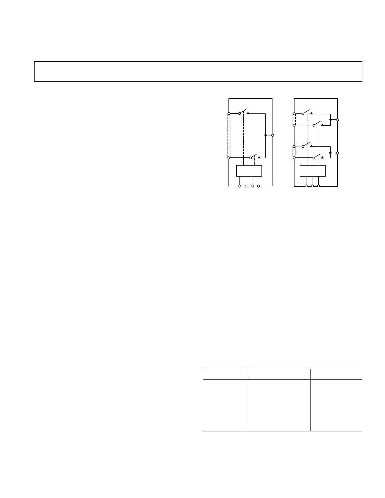
The ADG608 and ADG609 are monolithic CMOS analog multiplexers comprising eight single channels and four differential
channels respectively, fully specified for ± 5 V, +5 V and +3 V
power supplies. The ADG608 switches one of eight inputs to a
common output as determined by the 3-bit binary address lines
A0, A1 and A2. The ADG609 switches one of four differential
inputs to a common differential output as determined by the
2-bit binary address lines A0 and A1. An EN input on both devices is used to enable or disable the device. When disabled, all
channels are switched OFF. All the address and enable inputs
are TTL compatible over the full specified operating temperature range, making the parts suitable for bus-controlled systems
such as data acquisition systems, process controls, avionics and
ATEs since the TTL compatible address inputs simplify the digital
PRODUCT HIGHLIGHTS
1. Extended Signal Range
The ADG608/ADG609 are fabricated on an enhanced
LC
extends to the supplies.
2. Low Power Dissipation
3. Low R
4. Fast Switching Times
5. Break-Before-Make Switching
Switches are guaranteed break-before-make so that input
signals are protected against momentary shorting.
6. Single/Dual Supply Operation
interface design and reduce the board space requirements.
The ADG608/ADG609 are designed on an enhanced LC
process that provides low power dissipation yet gives high
switching speed and low on resistance. Each channel conducts
equally well in both directions when ON and has an input signal
range which extends to the supplies. In the OFF condition, signal levels up to the supplies are blocked. All channels exhibit
break-before-make switching action preventing momentary
shorting when switching channels. Inherent in the design is low
charge injection for minimum transients when switching the
digital inputs.
REV. A
Information furnished by Analog Devices is believed to be accurate and
reliable. However, no responsibility is assumed by Analog Devices for its
use, nor for any infringements of patents or other rights of third parties
which may result from its use. No license is granted by implication or
otherwise under any patent or patent rights of Analog Devices.
2
MOS
Model Temperature Range Package Option*
ADG608BN –40°C to +85°C N-16
ADG608BR – 40°C to +85°C R-16A
ADG608BRU – 40°C to +85°C RU-16
ADG608TRU – 55°C to +125°C RU-16
ADG609BN –40°C to +85°C N-16
ADG609BR –40°C to +85°C R-16A
ADG609BRU –40°C to +85°C RU-16
*N = Plastic DIP; RU = Thin Shrink Small Outline Package (TSSOP);
R = 0.15" Small Outline IC (SOIC).
One Technology Way, P.O. Box 9106, Norwood, MA 02062-9106, U.S.A.
Tel: 617/329-4700 Fax: 617/326-8703
FUNCTIONAL BLOCK DIAGRAMS
2
MOS process giving an increased signal range which
ON
ORDERING GUIDE
© Analog Devices, Inc., 1995
Page 2

ADG608/ADG609–SPECIFICA TIONS
1
DUAL SUPPLY
(VDD = +5 V 6 10%, VSS = –5 V 6 10%, GND = 0 V, unless otherwise noted)
Parameter B Version T Version
+258C –40°C to +258C –558C to Test Conditions/
+858C +1258C Units Comments
ANALOG SWITCH
Analog Signal Range V
R
ON
22 22 Ω typ –3.5 V < VS < +3.5 V, IS = –1 mA;
30 35 30 40 Ω max V
SS
to V
DD
VSS to V
DD
V
= +4.5 V, VSS = –4.5 V;
DD
Test Circuit 1
∆R
ON
Match 2 3 2 3 Ω max VS = 0 V, IDS = –1 mA;
R
ON
56 56 Ω max –3 V < VS < +3 V, IDS = –1 mA;
= +5 V, VSS = –5 V
V
DD
VDD = +5 V, VSS = –5 V
LEAKAGE CURRENTS V
Source OFF Leakage I
(OFF) ±0.05 ±0.05 nA typ VD = ±4.5 V, VS = 74.5 V;
S
= +5.5 V, VSS = –5.5 V
DD
±0.5 ±2 ±0.5 ±10 nA max Test Circuit 2
Drain OFF Leakage I
(OFF) ±0.05 ±0.05 nA typ VD = ±4.5 V, VS = 74.5 V;
D
ADG608 ±0.5 ±2 ±0.5 ±10 nA max Test Circuit 3
ADG609 ±0.5 ±1 ±0.5 ±5 nA max
Channel ON Leakage I
, IS (ON) ±0.05 ±0.05 nA typ VS = VD = ±4.5 V;
D
ADG608 ±0.5 ±3 ±0.5 ±20 nA max Test Circuit 4
ADG609 ±0.5 ±1.5 ±0.5 ±10 nA max
DIGITAL INPUTS
Input High Voltage, V
Input Low Voltage, V
INL
INH
2.4 2.4 V min
0.8 0.8 V max
Input Current
I
INL
or I
INH
±1 ±1 µA max VIN = 0 or V
CIN, Digital Input Capacitance 5 5 pF typ
DYNAMIC CHARACTERISTICS
t
TRANSITION
2
50 50 ns typ RL = 300 Ω, CL = 35 pF;
75 90 75 100 ns max V
= ±3.5 V, VS8 = 73.5 V;
S1
Test Circuit 5
t
OPEN
(EN) 50 50 ns typ RL = 300 Ω, CL = 35 pF;
t
ON
(EN) 30 30 ns typ RL = 300 Ω, CL = 35 pF;
t
OFF
Charge Injection 6 6 pC typ V
10 10 ns min RL = 300 Ω, CL = 35 pF;
= +3.5 V; Test Circuit 6
V
S
75 90 75 100 ns max V
45 60 45 75 ns max V
= +3.5 V; Test Circuit 7
S
= +3.5 V; Test Circuit 7
S
= 0 V, RS = 0 Ω, CL = 1 nF;
S
Test Circuit 8
OFF Isolation 85 85 dB typ R
Channel-to-Channel Crosstalk 85 85 dB typ R
= 1 kΩ, CL = 15 pF, f = 100 kHz;
L
= 3 V rms; Test Circuit 9
V
S
= 1 kΩ, CL = 15 pF, f = 100 kHz;
L
Test Circuit 10
(OFF) 9 9 pF typ
C
S
(OFF)
C
D
ADG608 40 40 pF typ
ADG609 20 20 pF typ
(ON)
C
D
ADG608 54 54 pF typ
ADG609 34 34 pF typ
DD
POWER REQUIREMENTS
I
DD
0.05 0.2 0.05 0.2 µA typ VIN = 0 V or V
0.2 2 0.2 2 µA max
I
SS
0.01 0.1 0.01 0.1 µA typ
0.1 1 0.1 1 µA m
NOTES
1
Temperature ranges are as follows: B Version: –40°C to +85°C; T Version: –55°C to +125°C.
2
Guaranteed by design, not subject to production test.
Specifications subject to change without notice.
–2–
DD
ax
REV. A
Page 3

SINGLE SUPPLY
1
(VDD = +5 V 6 10%, VSS = 0 V, GND = 0 V, unless otherwise noted)
ADG608/ADG609
Parameter B Version T Version
+258C –408C to +258C –558C to Test Conditions/
+858C +1258C Units Comments
ANALOG SWITCH
Analog Signal Range 0
R
ON
40 40 Ω typ VS = +3.5 V, IS = –1 mA;
50 60 50 70 Ω max V
to V
DD
0 to V
DD
V
= +4.5 V;
DD
Test Circuit 1
∆R
ON
Match 2 3 2 3 Ω max VS = 0 V, IDS = –1 mA;
R
ON
56 56 Ω max +1 V < VS < +3 V, IDS = –1 mA;
= +5 V
V
DD
VDD = +5 V
LEAKAGE CURRENTS V
Source OFF Leakage I
(OFF) ±0.05 ±0.05 nA typ VD = 4.5 V/0.1 V, VS = 0.1 V/4.5 V;
S
= +5.5 V
DD
±0.5 ±2 ±0.5 ±10 nA max Test Circuit 2
Drain OFF Leakage I
(OFF) ±0.05 ±0.05 nA typ VD = 4.5 V/0.1 V, VS = 0.1 V/4.5 V;
D
ADG608 ±0.5 ±2 ±0.5 ±10 nA max Test Circuit 3
ADG609 ±0.5 ±1 ±0.5 ±5 nA max
Channel ON Leakage I
, IS (ON) ±0.05 ±0.05 nA typ VS = VD = 4.5 V/0.1 V;
D
ADG608 ±0.5 ±3 ±0.5 ±20 nA max Test Circuit 4
ADG609 ±0.5 ±1.5 ±0.5 ±10 nA max
DIGITAL INPUTS
Input High Voltage, V
Input Low Voltage, V
INH
INL
2.4 2.4 V min
0.8 0.8 V max
Input Current
I
INL
or I
INH
±1 ±1 µA max VIN = 0 or V
CIN, Digital Input Capacitance 5 5 pF typ
DYNAMIC CHARACTERISTICS
t
TRANSITION
2
80 80 ns typ RL = 300 Ω, CL = 35 pF;
100 130 100 150 ns max V
= 3.5 V/0 V, VS8 = 0 V/3.5 V;
S1
Test Circuit 5
t
OPEN
(EN) 80 80 ns typ RL = 300 Ω, CL = 35 pF;
t
ON
(EN) 40 40 ns typ RL = 300 Ω, CL = 35 pF;
t
OFF
Charge Injection 0.5 0.5 pC typ V
10 10 ns min RL = 300 Ω, CL = 35 pF;
= +3.5 V; Test Circuit 6
V
S
100 130 100 150 ns max V
50 60 50 75 ns max V
= +3.5 V; Test Circuit 7
S
= +3.5 V; Test Circuit 7
S
= 0 V, RS = 0 Ω, CL = 1 nF;
S
3 3 pC max Test Circuit 8
OFF Isolation 85 85 dB typ R
Channel-to-Channel Crosstalk 85 85 dB typ R
= 1 kΩ, CL = 15 pF, f = 100 kHz;
L
= 1.5 V rms; Test Circuit 9
V
S
= 1 kΩ, CL = 15 pF, f = 100 kHz;
L
Test Circuit 10
(OFF) 9 9 pF typ
C
S
(OFF)
C
D
ADG608 40 40 pF typ
ADG609 20 20 pF typ
(ON)
C
D
ADG608 54 54 pF typ
ADG609 34 34 pF typ
DD
POWER REQUIREMENTS
I
DD
0.05 0.2 0.05 0.2 µA typ VIN = 0 V or V
0.2 2 0.2 2 µA max
NOTES
1
Temperature ranges are as follows: B Version: –40°C to +85°C; T Version: –55°C to +125°C.
2
Guaranteed by design, not subject to production test.
Specifications subject to change without notice.
REV. A
–3–
DD
Page 4

ADG608/ADG609–SPECIFICATIONS
1
SINGLE SUPPLY
Parameter B Version T Version
ANALOG SWITCH
Analog Signal Range 0
R
ON
RON Match 3 3 3 3 Ω max VS = 0 V, IDS = –1 mA, VDD = +3.3 V
(VDD = +3.3 V 6 10%, VSS = 0 V, GND = 0 V, unless otherwise noted)
+258C –408C to +258C –558C to Test Conditions/
60 60 Ω typ VS = +1.5 V, IS = –1 mA;
90 100 90 120 Ω max V
+858C +1258C Units Comments
to V
DD
0 to V
DD
V
= +3 V; Test Circuit 1
DD
LEAKAGE CURRENTS V
Source OFF Leakage I
(OFF) ±0.05 ±0.05 nA typ VD = 2.6 V/0.1 V, VS = 0.1 V/2.6 V;
S
= +3.6 V
DD
±0.5 ±2 ±0.5 ±10 nA max Test Circuit 2
Drain OFF Leakage I
(OFF) ±0.05 ±0.05 nA typ VD = 2.6 V/0.1 V, VS = 0.1 V/2.6 V;
D
ADG608 ±0.5 ±2 ±0.5 ±10 nA max Test Circuit 3
ADG609 ±0.5 ±1 ±0.5 ±5 nA max
Channel ON Leakage I
, IS (ON) ±0.05 ±0.05 nA typ VS = VD = 2.6 V/0.1 V;
D
ADG608 ±0.5 ±3 ±0.5 ±20 nA max Test Circuit 4
ADG609 ±0.5 ±1.5 ±0.5 ±10 nA max
DIGITAL INPUTS
Input High Voltage, V
Input Low Voltage, V
INL
INH
2.4 2.4 V min
0.8 0.8 V max
Input Current
I
INL
or I
INH
±1 ±1 µA max VIN = 0 or V
CIN, Digital Input Capacitance 5 5 pF typ
DYNAMIC CHARACTERISTICS
t
TRANSITION
2
120 120 ns typ RL = 300 Ω, CL = 35 pF;
170 225 170 250 ns max V
= 1.5 V/0 V, VS8 = 0 V/1.5 V;
S1
Test Circuit 5
t
OPEN
(EN) 120 120 ns typ RL = 300 Ω, CL = 35 pF;
t
ON
(EN) 40 40 ns typ RL = 300 Ω, CL = 35 pF;
t
OFF
Charge Injection 0.5 0.5 pC typ V
10 10 ns min RL = 300 Ω, CL = 35 pF;
= +1.5 V; Test Circuit 6
V
S
170 225 170 250 ns max V
60 75 60 90 ns max V
= +1.5 V; Test Circuit 7
S
= +1.5 V; Test Circuit 7
S
= 0 V, RS = 0 Ω, CL = 1 nF;
S
3 3 pC max Test Circuit 8
OFF Isolation 85 85 dB typ R
Channel-to-Channel Crosstalk 85 85 dB typ R
= 1 kΩ, CL = 15 pF, f = 100 kHz;
L
= 1 V rms; Test Circuit 9
V
S
= 1 kΩ, CL = 15 pF, f = 100 kHz;
L
Test Circuit 10
(OFF) 9 9 pF typ
C
S
(OFF)
C
D
ADG608 40 40 pF typ
ADG609 20 20 pF typ
(ON)
C
D
ADG608 54 54 pF typ
ADG609 34 34 pF typ
DD
POWER REQUIREMENTS
I
DD
0.05 0.2 0.05 0.2 µA typ VIN = 0 V or V
0.2 2 0.2 2 µA max
NOTES
1
Temperature ranges are as follows: B Version: –40°C to +85°C; T Version: –55°C to +125°C.
2
Guaranteed by design, not subject to production test.
Specifications subject to change without notice.
–4–
DD
REV. A
Page 5

ADG608/ADG609
ABSOLUTE MAXIMUM RATINGS
1
(TA = +25°C unless otherwise noted)
VDD to VSS . . . . . . . . . . . . . . . . . . . . . . . . . . . . . . . . . . +13 V
V
to GND . . . . . . . . . . . . . . . . . . . . . . . . . –0.3 V to +6.5 V
DD
V
to GND . . . . . . . . . . . . . . . . . . . . . . . . . +0.3 V to –6.5 V
SS
Analog, Digital Inputs
2
. . . . . . . . . . . . . . –0.3 V to VDD + 2 V
or 20 mA, Whichever Occurs First
Continuous Current, S or D . . . . . . . . . . . . . . . . . . . . 20 mA
Peak Current, S or D
(Pulsed at 1 ms, 10% Duty Cycle Max) . . . . . . . . . . 40 mA
Operating Temperature Range
Industrial (B Version) . . . . . . . . . . . . . . . . –40°C to +85°C
Extended (T Version) . . . . . . . . . . . . . . . –55°C to +125°C
Storage Temperature Range . . . . . . . . . . . . –65°C to +150°C
Junction Temperature . . . . . . . . . . . . . . . . . . . . . . . . +150°C
Plastic DIP Package
θ
, Thermal Impedance . . . . . . . . . . . . . . . . . . . . 117°C/W
JA
Lead Temperature, Soldering (10 sec) . . . . . . . . . . +260°C
Table I. ADG608 Truth Table
A2 A1 A0 EN ON SWITCH
X X X 0 NONE
00 0 1 1
00 1 1 2
01 0 1 3
01 1 1 4
10 0 1 5
10 1 1 6
11 0 1 7
11 1 1 8
X = Don’t Care
PIN CONFIGURATIONS
SOIC Package
θ
, Thermal Impedance . . . . . . . . . . . . . . . . . . . . . . 77°C/W
JA
Lead Temperature, Soldering
Vapor Phase (60 sec) . . . . . . . . . . . . . . . . . . . . . . +215°C
Infrared (15 sec) . . . . . . . . . . . . . . . . . . . . . . . . . . +220°C
TSSOP Package
θ
, Thermal Impedance . . . . . . . . . . . . . . . . . . . . . 158°C/W
JA
Lead Temperature, Soldering
Vapor Phase (60 sec) . . . . . . . . . . . . . . . . . . . . . . +215°C
Infrared (15 sec) . . . . . . . . . . . . . . . . . . . . . . . . . . +220°C
ESD Rating . . . . . . . . . . . . . . . . . . . . . . . . . . . . . . . . >5000 V
NOTES
1
Stresses above those listed under “Absolute Maximum Ratings” may cause
permanent damage to the device. This is a stress rating only and functional
operation of the device at these or any other conditions above those listed in the
operational sections of this specification is not implied. Exposure to absolute
maximum rating conditions for extended periods may affect device reliability.
Only one absolute maximum rating may be applied at any one time.
2
Overvoltages at A, S, D or EN will be clamped by internal diodes. Current should
be limited to the maximum ratings given.
Table II. ADG609 Truth Table
A1 A0 EN ON SWITCH PAIR
X X 0 NONE
00 11
01 12
10 13
11 14
X = Don’t Care
DIP/SOIC/TSSOP
1
A0
2
EN
V
3
SS
ADG608
S1
4
TOP VIEW
5
S2
(Not to Scale)
6
S3
7
S4
8
D
DIP/SOIC/TSSOP
1
16
A1
15
A2
GND
14
13
V
DD
12
S5
S6
11
10
S7
9
S8
EN
V
S1A
S2A
S3A
S4A
DA
A0
SS
2
3
ADG609
4
TOP VIEW
5
(Not to Scale)
6
7
8
16
A1
15
GND
V
14
DD
13
S1B
12
S2B
S3B
11
10
S4B
9
DB
REV. A
–5–
Page 6

ADG608/ADG609–Typical Performance Characteristics
100
ON RESISTANCE – Ω
90
0
0.0 5.00.5 2.5 4.0 4.5
50
30
20
10
80
60
40
70
1.0 1.5 2.0 3.0 3.5
VD (VS) – Volts
VDD = +3V
V
SS
= 0V
VDD = +5V
V
SS
= 0V
TA = +25oC
100
ON RESISTANCE – Ω
90
0
0.0 5.00.5 2.5 4.0 4.5
50
30
20
10
80
60
40
70
1.0 1.5 2.0 3.0 3.5
V
D
(VS) – Volts
VDD = +5V
V
SS
= 0V
+125oC
+85oC
+25oC
VS, VD – Volts
0.03
0.00
–0.03
–5 5–4
LEAKAGE CURRENTS – nA
–3 –2 –1 0 1 2 3 4
0.02
0.01
–0.01
–0.02
ID(OFF)
ID(ON)
IS(OFF)
VDD = +5V
V
SS
= –5V
T
A
= +25
o
C
50
TA = +25oC
45
40
35
30
25
20
ON RESISTANCE – Ω
15
10
5
0
–5.0 5.0–4.0 0.0 3.0 4.0–3.0 –2.0 –1.0 1.0 2.0
(VS) – Volts
V
D
VDD = +3V
V
= –3V
SS
VDD = +5V
V
= –5V
SS
Figure 1. RON as a Function of VD (VS): Dual Supply Voltage
50
VDD = +5V
45
V
= –5V
SS
40
35
30
25
20
ON RESISTANCE – Ω
15
10
5
0
–5.0 5.0–4.0 0.0 3.0 4.0
–3.0 –2.0 –1.0 1.0 2.0
Figure 2. RON as a Function of VD (VS) for Different
Temperatures
100
VDD = +3V
90
V
= 0V
SS
80
70
60
50
40
ON RESISTANCE – Ω
30
20
10
0
0.0 3.00.5 1.5
1.0 2.52.0
Figure 3. RON as a Function of VD (VS) for Different
Temperatures
(VS) – Volts
V
D
VD (VS) – Volts
+125oC
+85oC
+25oC
+125oC
+85oC
+25oC
Figure 4. RON as a Function of VD (VS): Single Supply Voltage
Figure 5. RON as a Function of VD (VS) for Different
Temperatures
Figure 6. Leakage Currents as a Function of VD (VS)
–6–
REV. A
Page 7

0.02
VS, VD – Volts
0.02
0.01
–0.01
0 3.00.5
LEAKAGE CURRENTS – nA
1.0 1.5 2.0 2.5
0.00
ID(OFF)
I
D
(ON)
I
S
(OFF)
VDD = +3V
V
SS
= 0V
T
A
= +25oC
VDD = +5V
V
= 0V
SS
T
= +25oC
A
0.01
0.00
LEAKAGE CURRENTS – nA
–0.01
051234
VS,VD – Volts
(OFF)
I
D
ID(ON)
I
(OFF)
S
ADG608/ADG609
Figure 7. Leakage Currents as a Function of VD (VS)
4
10
VDD = +5V
V
= –5V
SS
3
10
2
10
– µA
DD
I
1
10
0
10
–1
10
10 10M100 1k 10k 100k 1M
EN = 2.4V
EN = 0V
FREQUENCY – Hz
Figure 8. Positive Supply Current vs. Switching Frequency
30
CL = 1nF
20
Figure 10. Leakage Currents as a Function of VD (VS)
4
10
VDD = +5V
V
= –5V
SS
3
10
2
10
1
10
– µA
SS
I
0
10
–1
10
–2
10
10 10M100 1k 10k 100k 1M
EN = 2.4V
EN = 0V
FREQUENCY – Hz
Figure 11. Negative Supply Current vs. Switching Frequency
120
110
100
VDD = +5V
V
= –5V
SS
Figure 9. Charge Injection vs. Analog Voltage V
REV. A
10
VDD = +5V
V
= –5V
SS
0
CHARGE INJECTION – pC
–10
–5 5–4
–3 –2 –1 0 1 2 3 4
SOURCE VOLTAGE – V
VDD = +3V
V
= 0V
SS
VDD = +5V
V
= 0V
SS
90
dB
80
70
60
50
100 1M1k
S
Figure 12. Crosstalk and Off Isolation vs. Frequency
10k 100k
FREQUENCY – Hz
–7–
Page 8

ADG608/ADG609
V
D
S1
S2
S8
V
S
V
SS
V
DD
I
D
(OFF)
V
SS
V
DD
+0.8V
D
EN
A
GND
Test Circuits
I
DS
V1
S
V
S
R
= V1/I
ON
Test Circuit 1. On Resistance
I
(OFF)
S
A
V
S
S1
S2
S8
V
D
Test Circuit 2. IS (OFF)
V
DD
V
DD
A2
V
IN
50Ω
+2.4V
A1
A0
EN
S2 THRU S7
ADG608*
V
DD
V
GND
D
DS
Test Circuit 3. ID (OFF)
V
SS
V
SS
DD
D
GND
EN
+0.8V
V
S
V
S1
S8
V
DD
V
DD
GND
SS
V
SS
I
(ON)
D
D
A
V
D
EN
+2.4V
Test Circuit 4. ID (ON)
V
SS
V
SS
V
S1
S1
V
S8
S8
D
R
300Ω
C
L
L
35pF
DRIVE (V
V
OUT
ADDRESS
IN
V
OUT
3V
)
0V
50%
90%
50%
90%
* SIMILAR CONNECTION FOR ADG609
Test Circuit 5. Switching Time of Multiplexer, t
t
TRANSITION
TRANSITION
–8–
t
TRANSITION
REV. A
Page 9

ADG608/ADG609
V
V
V
A2
V
IN
50Ω
+2.4V
* SIMILAR CONNECTION FOR ADG609
A1
A0
EN
DD
DD
S2 THRU S7
ADG608
GND
SS
V
SS
S1
*
S8
D
R
L
300Ω
V
S
C
L
35pF
DRIVE (V
V
OUT
ADDRESS
V
OUT
3V
)
IN
0V
t
OPEN
80%
80%
V
DD
V
DD
A2
A1
A0
ADG608
EN
V
50Ω
IN
* SIMILAR CONNECTION FOR ADG609
V
V
A2
A1
R
S
V
S
V
IN
A0
S
EN
V
SS
V
SS
S2 THRU S8
*
GND
DD
DD
ADG608*
GND
Test Circuit 6. Break-Before-Make Delay, t
3V
ENABLE
S1
V
S
D
R
300Ω
C
L
L
35pF
DRIVE (V
V
OUT
OUTPUT
)
IN
0V
V
0
0V
Test Circuit 7. Enable Delay, tON (EN), t
V
SS
V
SS
D
C
1nF
V
OUT
L
LOGIC
INPUT (V
V
IN
OUT
3V
)
0V
OFF
OPEN
50%
(EN)
0.9V
Q
INJ
0
t
(EN)
ON
= CL x ∆V
50%
OUT
0.9V
∆ V
t
OFF
(EN)
0
OUT
REV. A
* SIMILAR CONNECTION FOR ADG609
Test Circuit 8. Charge Injection
–9–
Page 10

ADG608/ADG609
A2
V
OUT
V
SS
V
DD
D
A1
A0
EN
GND
ADG608
R
L
1kΩ
V
SS
V
DD
S1
V
S
S2
S8
2.4V
1kΩ
A2
A1
A0
EN
GND
V
DD
V
DD
ADG608
S1
S8
D
R
V
SS
V
SS
1kΩ
L
V
S
V
OUT
Test Circuit 9. OFF Isolation
TERMINOLOGY
V
DD
V
SS
Most positive power supply potential.
Most negative power supply potential in dual
supplies. In single supply applications, it may
be connected to ground.
GND Ground (0 V) reference.
R
∆R
ON
ON
Ohmic resistance between D and S.
RON variation due to a change in the analog
input voltage with a constant load current.
R
Match Difference between the RON of any two
ON
channels.
I
(OFF) Source leakage current when the switch is off.
S
(OFF) Drain leakage current when the switch is off.
I
D
, IS (ON) Channel leakage current when the switch is
I
D
on.
V
, V
D
S
(OFF) Channel input capacitance for “OFF”
C
S
Analog voltage on terminals D, S.
condition.
C
(OFF) Channel output capacitance for “OFF”
D
condition.
C
, CS (ON) “ON” switch capacitance.
D
C
IN
(EN) Delay time between the 50% and 90% points
t
ON
Digital input capacitance.
of the digital input and switch “ON”
condition.
Test Circuit 10. Channel-to-Channel Crosstalk
t
(EN) Delay time between the 50% and 90% points
OFF
of the digital input and switch “OFF”
condition.
t
TRANSITION
Delay time between the 50% and 90% points
of the digital inputs and the switch “ON”
condition when switching from one address
state to another.
t
OPEN
“OFF” time measured between the 80%
points of both switches when switching from
one address state to another.
V
V
I
INL
INH
INL
(I
) Input current of the digital input.
INH
Maximum input voltage for logic “0.”
Minimum input voltage for logic “1.”
Crosstalk A measure of unwanted signal which is
coupled through from one channel to another
as a result of parasitic capacitance.
Off Isolation A measure of unwanted signal coupling
through an “OFF” channel.
Charge Injection A measure of the glitch impulse transferred
from the digital input to the analog output
during switching.
I
DD
I
SS
Positive supply current.
Negative supply current.
–10–
REV. A
Page 11

OUTLINE DIMENSIONS
Dimensions shown in inches and (mm).
16-Pin Plastic (N-16)
ADG608/ADG609
PIN 1
0.210
(5.33)
0.200 (5.05)
0.125 (3.18)
16
18
0.840 (21.33)
0.745 (18.93)
0.022 (0.558)
0.014 (0.356)
0.100
(2.54)
BSC
0.070 (1.77)
0.045 (1.15)
9
0.280 (7.11)
0.240 (6.10)
0.060 (1.52)
0.015 (0.38)
0.150
(3.81)
SEATING
PLANE
16-Pin SOIC (R-16A)
0.3937 (10.00)
0.3859 (9.80)
PLANE
16 9
PIN 1
0.0192 (0.49)
0.0500
(1.27)
0.0138 (0.35)
BSC
0.2440 (6.20)
81
0.2284 (5.80)
0.0688 (1.75)
0.0532 (1.35)
0.0099 (0.25)
0.0075 (0.19)
8°
0°
0.1574 (4.00)
0.1497 (3.80)
0.0098 (0.25)
0.0040 (0.10)
SEATING
0.325 (8.25)
0.300 (7.62)
0.015 (0.381)
0.008 (0.204)
0.0196 (0.50)
0.0099 (0.25)
0.0500 (1.27)
0.0160 (0.41)
0.195 (4.95)
0.115 (2.93)
x 45°
REV. A
0.177 (4.50)
0.006 (0.15)
0.002 (0.05)
SEATING
PLANE
16-Pin TSSOP (RU-16)
0.201 (5.10)
0.193 (4.90)
16 9
0.169 (4.30)
1
PIN 1
0.0118 (0.30)
0.0256
(0.65)
0.0075 (0.19)
BSC
8
–11–
0.256 (6.50)
0.246 (6.25)
0.0433
(1.10)
MAX
0.0079 (0.20)
0.0035 (0.090)
8°
0°
0.028 (0.70)
0.020 (0.50)
Page 12

C2021a–18–4/96
–12–
PRINTED IN U.S.A.
 Loading...