

Page 1
High Voltage Latch-Up Proof,
FEATURES
Latch-up proof
8 kV HBM ESD rating
Low on resistance (<10 Ω)
±9 V to ±22 V dual-supply operation
9 V to 40 V single-supply operation
48 V supply maximum ratings
Fully specified at ±15 V, ±20 V, +12 V, and +36 V
V
to VDD analog signal range
SS
APPLICATIONS
Relay replacement
Automatic test equipment
Data acquisition
Instrumentation
Avio nics
Audio and video switching
Communication systems
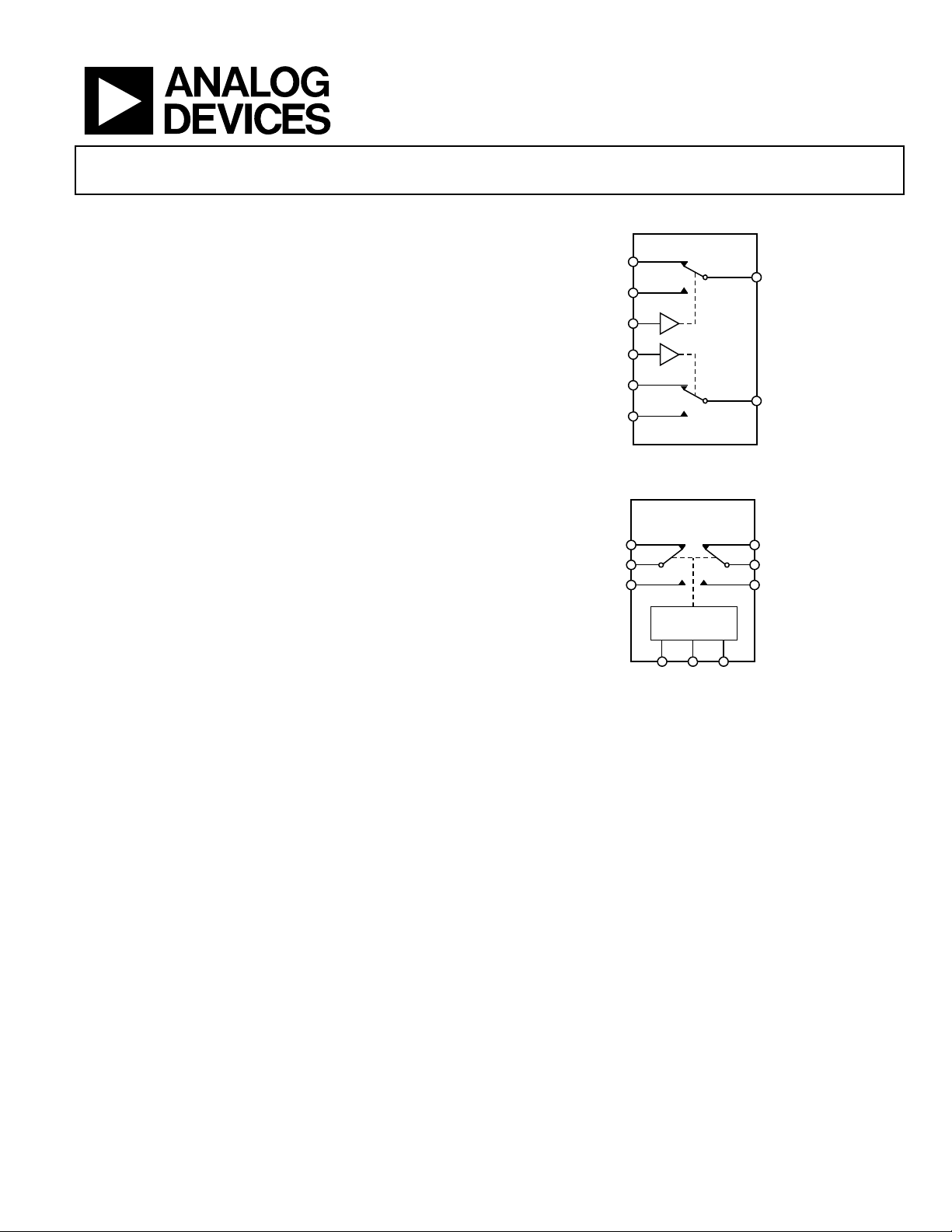
Dual SPDT Switches
ADG5436
FUNCTIONAL BLOCK DIAGRAMS
S1A
S1B
IN1
IN2
S2A
S2B
SWITCHES SHOWN FOR A LOGIC 1 I NP UT.
S1A
D1
S1B
ADG5436
Figure 1. TSSOP Package
ADG5436
D1
D2
S2A
D2
S2B
09204-001
GENERAL DESCRIPTION
The ADG5436 is a monolithic CMOS device containing two
independently selectable single-pole/single-throw (SPDT)
switches. An EN input on the LFCSP package enables or
disables the device. When disabled, all channels switch off. Each
switch conducts equally well in both directions when on and
has an input signal range that extends to the supplies. In the off
condition, signal levels up to the supplies are blocked. Both
switches exhibit break-before-make switching action for use in
multiplexer applications.
The on-resistance profile is very flat over the full analog input
range, ensuring excellent linearity and low distortion when
switching audio signals.
LOGIC
IN2 ENIN1
SWITCHES S HO WN FOR A LOGIC 1 INPUT.
Figure 2. LFCSP Package
09204-002
PRODUCT HIGHLIGHTS
1. Trench isolation guards against latch-up. A dielectric trench
separates the P and N channel transistors thereby preventing
latch-up even under severe overvoltage conditions.
2. Low R
3. Dual-supply operation. For applications where the analog
signal is bipolar, the ADG5436 can be operated from dual
supplies up to ±22 V.
4. Single-supply operation. For applications where the analog
signal is unipolar, the ADG5436 can be operated from a
single-rail power supply up to 40 V.
5. 3 V logic compatible digital inputs: V
6. No V
.
ON
logic power supply required.
L
= 2.0 V, V
INH
= 0.8 V.
INL
Rev. A
Information furnished by Analog Devices is believed to be accurate and reliable. However, no
responsibility is assumed by Analog Devices for its use, nor for any infringements of patents or other
rights of third parties that may result from its use. Specifications subject to change without notice. No
license is granted by implication or otherwise under any patent or patent rights of Analog Devices.
Trademarks and registered trademarks are the property of their respective owners.
One Technology Way, P.O. Box 9106, Norwood, MA 02062-9106, U.S.A.
Tel: 781.329.4700 www.analog.com
Fax: 781.461.3113 ©2010–2011 Analog Devices, Inc. All rights reserved.
Page 2

ADG5436
TABLE OF CONTENTS
Features .............................................................................................. 1
Applications ....................................................................................... 1
Functional Block Diagrams ............................................................. 1
General Description ......................................................................... 1
Product Highlights ........................................................................... 1
Revision History ............................................................................... 2
Specifications ..................................................................................... 3
±15 V Dual Supply ....................................................................... 3
±20 V Dual Supply ....................................................................... 4
12 V Single Supply ........................................................................ 5
36 V Single Supply ........................................................................ 6
Continuous Current per Channel, Sx or Dx ............................. 7
REVISION HISTORY
6/11—Rev. 0 to Rev. A
Added I
Updated Outline Dimensions ....................................................... 19
Changes to Ordering Guide .......................................................... 19
7/10—Revision 0: Initial Version
−40°C to +125°C Parameter .......................................... 5
SS
Absolute Maximum Ratings ............................................................8
ESD Caution...................................................................................8
Pin Configurations and Function Descriptions ............................9
Truth Table For Switches ..............................................................9
Typical Performance Characteristics ........................................... 10
Test Circuits ..................................................................................... 14
Terminology .................................................................................... 16
Trench Isolation .............................................................................. 17
Applications Information .............................................................. 18
Outline Dimensions ....................................................................... 19
Ordering Guide .......................................................................... 19
Rev. A | Page 2 of 20
Page 3

ADG5436
SPECIFICATIONS
±15 V DUAL SUPPLY
VDD = +15 V ± 10%, VSS = −15 V ± 10%, GND = 0 V, unless otherwise noted.
Table 1.
Parameter 25°C −40°C to +85°C −40°C to +125°C Unit Test Conditions/Comments
ANALOG SWITCH
Analog Signal Range VDD to VSS V
On Resistance, RON 9.8 Ω typ VS = ±10 V, IS = −10 mA; see Figure 25
11 14 16 Ω max VDD = +13.5 V, VSS = −13.5 V
On-Resistance Match
Between Channels, ∆R
ON
0.35 Ω typ V
0.7 0.9 1.1 Ω max
On-Resistance Flatness, R
1.2 Ω typ VS = ±10 V, IS = −10 mA
FL AT (ON)
1.6 2 2.2 Ω max
LEAKAGE CURRENTS
Source Off Leakage, IS (Off )
Drain Off Leakage, ID (Off )
Channel On Leakage, ID (On), IS (On)
DIGITAL INPUTS
Input High Voltage, V
Input Low Voltage, V
Input Current, I
INL
2.0 V min
INH
0.8 V max
INL
or I
0.002 µA typ VIN = V
INH
±0.05
±0.25 ±0.75 ±3.5
±0.1
±0.4 ±2 ±12
±0.1
±0.4 ±2 ±12
VDD = +16.5 V, VSS = −16.5 V
nA typ
nA max
nA typ
nA max
nA typ VS = VD = ±10 V; see Figure 24
nA max
±0.1 µA max
Digital Input Capacitance, CIN 5 pF typ
DYNAMIC CHARACTERISTICS1
Transition Time, t
170 ns typ RL = 300 Ω, CL = 35 pF
TRANSITION
235 285 316 ns max VS = 10 V; see Figure 31
tON 173 ns typ RL = 300 Ω, CL = 35 pF
230 280 351 ns max VS = 10 V; see Figure 33
t
124 ns typ RL = 300 Ω, CL = 35 pF
OFF
160 193 218 ns max VS = 10 V; see Figure 33
Break-Before-Make Time Delay, tD 55 ns typ RL = 300 Ω, CL = 35 pF
18 ns min VS1 = VS2 = 10 V; see Figure 32
Charge Injection, Q
200 pC typ VS = 0 V, RS = 0 Ω, CL = 1 nF;
INJ
Off Isolation −78 dB typ RL = 50 Ω, CL = 5 pF, f = 1 MHz;
Channel-to-Channel Crosstalk −58 dB typ RL = 50 Ω, CL = 5 pF, f = 1 MHz;
Total Harmonic Distortion + Noise 0.009 % typ RL = 1 kΩ, 15 V p-p, f = 20 Hz to 20 kHz;
−3 dB Bandwidth 102 MHz typ RL = 50 Ω, CL = 5 pF; see Figure 30
Insertion Loss −0.7 dB typ RL = 50 Ω, CL = 5 pF, f = 1 MHz;
CS (Off ) 18 pF typ VS = 0 V, f = 1 MHz
CD (Off ) 62 pF typ VS = 0 V, f = 1 MHz
CD (On), CS (On) 83 pF typ VS = 0 V, f = 1 MHz
= ±10 V , IS = −10 mA
S
V
= ±10 V, VD = 10 V; see Figure 28
S
V
= ±10 V, VD = 10 V; see Figure 28
S
or VDD
GND
see Figure 34
see Figure 27
see Figure 26
see Figure 29
see Figure 30
Rev. A | Page 3 of 20
Page 4

ADG5436
Parameter 25°C −40°C to +85°C −40°C to +125°C Unit Test Conditions/Comments
POWER REQUIREMENTS VDD = +16.5 V, VSS = −16.5 V
IDD
ISS
VDD/VSS ±9/±22 V min/V max GND = 0 V
1
Guaranteed by design; not subject to production test.
±20 V DUAL SUPPLY
VDD = +20 V ± 10%, VSS = −20 V ± 10%, GND = 0 V, unless otherwise noted.
Table 2.
Parameter 25°C −40°C to +85°C −40°C to +125°C Unit Test Conditions/Comments
ANALOG SWITCH
Analog Signal Range VDD to VSS V
On Resistance, RON
On-Resistance Match
Between Channels, ∆R
On-Resistance Flatness, R
LEAKAGE CURRENTS
Source Off Leakage, IS (Off )
Drain Off Leakage, ID (Off )
Channel On Leakage, ID (On), IS (On)
DIGITAL INPUTS
Input High Voltage, V
Input Low Voltage, V
Input Current, I
or I
INL
±0.1 µA max
Digital Input Capacitance, CIN 5 pF typ
DYNAMIC CHARACTERISTICS1
Transition Time, t
TRANSITION
217 260 293 ns max VS = 10 V; see Figure 31
tON 164 ns typ RL = 300 Ω, CL = 35 pF
213 256 287 ns max VS = 10 V; see Figure 33
t
110 ns typ RL = 300 Ω, CL = 35 pF
OFF
152 173 194 ns max VS = 10 V; see Figure 33
Break-Before-Make Time Delay, tD 50 ns typ RL = 300 Ω, CL = 35 pF
15 ns min VS1 = VS2 = 10 V; see Figure 32
Charge Injection, Q
Off Isolation −78 dB typ RL = 50 Ω, CL = 5 pF, f = 1 MHz;
Channel-to-Channel Crosstalk −58 dB typ RL = 50 Ω, CL = 5 pF, f = 1 MHz;
Total Harmonic Distortion + Noise 0.007 % typ RL = 1 kΩ, 20 V p-p, f = 20 Hz to 20 kHz;
−3 dB Bandwidth 100 MHz typ RL = 50 Ω, CL = 5 pF; see Figure 30
ON
FL AT (ON)
2.0 V min
INH
0.8 V max
INL
0.002 µA typ VIN = V
INH
158 ns typ RL = 300 Ω, CL = 35 pF
250 pC typ VS = 0 V, RS = 0 Ω, CL = 1 nF; see
INJ
45
55 70
0.001
1
9
10 13 15
0.35
0.7 0.9 1.1
1.5
1.8 2.2 2.5
±0.05
±0.25 ±0.75 ±3.5
±0.1
±0.4 ±2 ±12
±0.1
±0.4 ±2 ±12
µA typ Digital inputs = 0 V or VDD
µA max
µA typ Digital inputs = 0 V or VDD
µA max
Ω typ VS = ±15 V, IS = −10 mA; see Figure 25
Ω max VDD = +18 V, VSS = −18 V
Ω typ VS = ±15 V , IS = −10 mA
Ω max
Ω typ VS = ±15 V, IS = −10 mA
Ω max
VDD = +22 V, VSS = −22 V
nA typ
V
= ±15 V, VD = 15 V; see Figure 28
S
nA max
nA typ
V
= ±15 V, VD = 15 V; see Figure 28
S
nA max
nA typ VS = VD = ±15 V; see Figure 24
nA max
or VDD
GND
Figure 34
see Figure 27
see Figure 26
see Figure 29
Rev. A | Page 4 of 20
Page 5

ADG5436
Parameter 25°C −40°C to +85°C −40°C to +125°C Unit Test Conditions/Comments
Insertion Loss −0.6 dB typ
CS (Off) 18 pF typ VS = 0 V, f = 1 MHz
CD (Off) 63 pF typ VS = 0 V, f = 1 MHz
CD (On), CS (On) 82 pF typ VS = 0 V, f = 1 MHz
POWER REQUIREMENTS VDD = +22 V, VSS = −22 V
IDD
ISS
50
70 110
0.001
1
μA typ Digital inputs = 0 V or VDD
μA max
μA typ Digital inputs = 0 V or VDD
μA max
VDD/VSS ±9/±22 V min/V max GND = 0 V
1
Guaranteed by design; not subject to production test.
12 V SINGLE SUPPLY
VDD = 12 V ± 10%, VSS = 0 V, GND = 0 V, unless otherwise noted.
Table 3.
Parameter 25°C −40°C to +85°C −40°C to +125°C Unit Test Conditions/Comments
ANALOG SWITCH
Analog Signal Range 0 V to VDD V
On Resistance, RON
On-Resistance Match
Between Channels, ∆R
ON
On-Resistance Flatness, R
FLAT (ON)
LEAKAGE CURRENTS
Source Off Leakage, IS (Off)
Drain Off Leakage, ID (Off)
Channel On Leakage, ID (On), IS (On)
DIGITAL INPUTS
Input High Voltage, V
Input Low Voltage, V
Input Current, I
INL
2.0 V min
INH
0.8 V max
INL
or I
0.002 μA typ VIN = V
INH
±0.1 μA max
Digital Input Capacitance, CIN 5 pF typ
DYNAMIC CHARACTERISTICS1
Transition Time, t
250 ns typ RL = 300 Ω, CL = 35 pF
TRANSITION
346 437 501 ns max VS = 8 V; see Figure 31
tON 250 ns typ RL = 300 Ω, CL = 35 pF
358 445 512 ns max VS = 8 V; see Figure 33
t
135 ns typ RL = 300 Ω, CL = 35 pF
OFF
178 212 237 ns max VS = 8 V; see Figure 33
Break-Before-Make Time Delay, tD 125 ns typ RL = 300 Ω, CL = 35 pF
50 ns min VS1 = VS2 = 8 V; see Figure 32
Charge Injection, Q
80 pC typ
INJ
19
22 27 31
0.4
0.8 1 1.2
4.4
5.5 6.5 7.5
±0.05
±0.25 ±0.75 ±3.5
±0.1
±0.4 ±2 ±12
±0.1
±0.4 ±2 ±12
Ω typ
Ω max VDD = 10.8 V, VSS = 0 V
Ω typ VS = 0 V to 10 V, IS = −10 mA
Ω max
Ω typ VS = 0 V to 10 V, IS = −10 mA
Ω max
V
nA typ
nA max
nA typ
nA max
nA typ VS = VD = 1 V/10 V; see Figure 24
nA max
Rev. A | Page 5 of 20
= 50 Ω, CL = 5 pF, f = 1 MHz;
R
L
see Figure 30
= 0 V to 10 V, IS = −10 mA; see
V
S
Figure 25
= 13.2 V, VSS = 0 V
DD
= 1 V/10 V, VD = 10 V/1 V;
V
S
see Figure 28
= 1 V/10 V, VD = 10 V/1 V;
V
S
see Figure 28
or VDD
GND
= 6 V, RS = 0 Ω, CL = 1 nF; see
V
S
Figure 34
Page 6

ADG5436
Parameter 25°C −40°C to +85°C −40°C to +125°C Unit Test Conditions/Comments
Off Isolation −78 dB typ
Channel-to-Channel Crosstalk −58 dB typ
Total Harmonic Distortion + Noise 0.075 % typ
−3 dB Bandwidth 106 MHz typ RL = 50 Ω, CL = 5 pF; see Figure 30
Insertion Loss −1.3 dB typ
CS (Off) 22 pF typ VS = 6 V, f = 1 MHz
CD (Off) 67 pF typ VS = 6 V, f = 1 MHz
CD (On), CS (On) 85 pF typ VS = 6 V, f = 1 MHz
POWER REQUIREMENTS VDD = 13.2 V
IDD
40
50 65
μA typ Digital inputs = 0 V or VDD
μA max
VDD 9/40 V min/V max GND = 0 V, VSS = 0 V
1
Guaranteed by design; not subject to production test.
36 V SINGLE SUPPLY
VDD = 36 V ± 10%, VSS = 0 V, GND = 0 V, unless otherwise noted.
= 50 Ω, CL = 5 pF, f = 1 MHz;
R
L
see Figure 27
= 50 Ω, CL = 5 pF, f = 1 MHz;
R
L
see Figure 26
= 1 kΩ, 6 V p-p, f = 20 Hz to 20 kHz;
R
L
see Figure 29
= 50 Ω, CL = 5 pF, f = 1 MHz;
R
L
see Figure 30
Table 4.
Parameter 25°C −40°C to +85°C −40°C to +125°C Unit Test Conditions/Comments
ANALOG SWITCH
Analog Signal Range 0 V to VDD V
On Resistance, RON
10.6
Ω typ
= 0 V to 30 V, IS = −10 mA;
V
S
see Figure 25
On-Resistance Match
Between Channels, ∆R
On-Resistance Flatness, R
LEAKAGE CURRENTS
Source Off Leakage, IS (Off)
ON
FLAT(ON)
12 15 17
0.35
0.7 0.9 1.1
2.7
3.2 3.8 4.5
±0.05
Ω max VDD = 32.4 V, VSS = 0 V
Ω typ VS = 0 V to 30 V, IS = −10 mA
Ω max
Ω typ VS = 0 V to 30 V, IS = −10 mA
Ω max
V
nA typ
= 39.6 V, VSS = 0 V
DD
= 1 V/30 V, VD = 30 V/1 V;
V
S
see Figure 28
Drain Off Leakage, ID (Off)
±0.25 ±0.75 ±3.5
±0.1
nA max
nA typ
= 1 V/30 V, VD = 30 V/1 V;
V
S
see Figure 28
Channel On Leakage, ID (On), IS (On)
±0.4 ±2 ±12
±0.1
±0.4 ±2 ±12
nA max
nA typ VS = VD = 1 V/30 V; see Figure 24
nA max
DIGITAL INPUTS
Input High Voltage, V
Input Low Voltage, V
Input Current, I
INL
2.0 V min
INH
0.8 V max
INL
or I
0.002 μA typ VIN = V
INH
GND
or VDD
±0.1 μA max
Digital Input Capacitance, CIN 5 pF typ
DYNAMIC CHARACTERISTICS1
Transition Time, t
174 ns typ RL = 300 Ω, CL = 35 pF
TRANSITION
246 270 303 ns max VS = 18 V; see Figure 31
tON 180 ns typ RL = 300 Ω, CL = 35 pF
247 270 301 ns max VS = 18 V; see Figure 33
Rev. A | Page 6 of 20
Page 7

ADG5436
Parameter 25°C −40°C to +85°C −40°C to +125°C Unit Test Conditions/Comments
t
127 ns typ RL = 300 Ω, CL = 35 pF
OFF
179 193 215 ns max VS = 18 V; see Figure 33
Break-Before-Make Time Delay, tD 55 ns typ RL = 300 Ω, CL = 35 pF
18 ns min VS1 = VS2 = 18 V; see Figure 32
Charge Injection, Q
Off Isolation −78 dB typ RL = 50 Ω, CL = 5 pF, f = 1 MHz;
Channel-to-Channel Crosstalk −58 dB typ RL = 50 Ω, CL = 5 pF, f = 1 MHz;
Total Harmonic Distortion + Noise 0.03 % typ RL = 1 kΩ, 18 V p-p, f = 20 Hz to
−3 dB Bandwidth 98 MHz typ RL = 50 Ω, CL = 5 pF; see Figure 30
Insertion Loss −0.8 dB typ RL = 50 Ω, CL = 5 pF, f = 1 MHz;
CS (Off ) 19 pF typ VS = 18 V, f = 1 MHz
CD (Off ) 40 pF typ VS = 18 V, f = 1 MHz
CD (On), CS (On) 78 pF typ VS = 18 V, f = 1 MHz
POWER REQUIREMENTS VDD = 39.6 V
IDD
VDD 9/40 V min/V max GND = 0 V, VSS = 0 V
1
Guaranteed by design; not subject to production test.
250 pC typ VS = 18 V, RS = 0 Ω, CL = 1 nF;
INJ
see Figure 34
see Figure 27
see Figure 26
20 kHz; see Figure 29
see Figure 30
80
100 130
µA typ Digital inputs = 0 V or VDD
µA max
CONTINUOUS CURRENT PER CHANNEL, Sx OR Dx
Table 5.
Parameter 25°C 85°C 125°C Unit
CONTINUOUS CURRENT, Sx OR Dx
VDD = +15 V, VSS = −15 V
TSSOP (θJA = 112.6°C/W) 122 77 44 mA maximum
LFCSP (θJA = 30.4°C/W) 217 116 53 mA maximum
VDD = +20 V, VSS = −20 V
TSSOP (θJA = 112.6°C/W) 130 80 45 mA maximum
LFCSP (θJA = 30.4°C/W) 229 121 54 mA maximum
VDD = 12 V, VSS = 0 V
TSSOP (θJA = 112.6°C/W) 84 56 36 mA maximum
LFCSP (θJA = 30.4°C/W) 150 90 48 mA maximum
VDD = 36 V, VSS = 0 V
TSSOP (θJA = 112.6°C/W) 110 70 42 mA maximum
LFCSP (θJA = 30.4°C/W) 196 109 52 mA maximum
Rev. A | Page 7 of 20
Page 8

ADG5436
ABSOLUTE MAXIMUM RATINGS
TA = 25°C, unless otherwise noted.
Table 6.
Parameter Rating
VDD to VSS 48 V
VDD to GND −0.3 V to +48 V
VSS to GND +0.3 V to −48 V
Analog Inputs1 VSS − 0.3 V to VDD + 0.3 V or
30 mA, whichever occurs first
Digital Inputs1 VSS − 0.3 V to VDD + 0.3 V or
30 mA, whichever occurs first
Peak Current, Sx or Dx Pins 375 mA (pulsed at 1 ms,
10% duty cycle maximum)
Continuous Current, Sx or Dx2 Data + 15%
Temperature Range
Operating −40°C to +125°C
Storage −65°C to +150°C
Junction Temperature 150°C
Thermal Impedance, θJA
16-Lead TSSOP (4-Layer
Board)
16-Lead LFCSP 30.4°C/W
Reflow Soldering Peak
Temperature, Pb Free
1
Overvoltages at the INx, Sx, and Dx pins are clamped by internal diodes.
Current should be limited to the maximum ratings given.
2
See Table 5.
112°C/W
260(+0/−5)°C
Stresses above those listed under Absolute Maximum Ratings
may cause permanent damage to the device. This is a stress
rating only; functional operation of the device at these or any
other conditions above those indicated in the operational
section of this specification is not implied. Exposure to absolute
maximum rating conditions for extended periods may affect
device reliability.
Only one absolute maximum rating can be applied at any
one time.
ESD CAUTION
Rev. A | Page 8 of 20
Page 9

ADG5436
IN1
1
S1A
2
D1
3
S1B
4
NC
16
NC
15
NC
14
V
DD
13
V
SS
5
S2B
12
GND
6
D2
11
NC
7
S2A
10
NC
8
IN2
9
NC = NO CONNECT
ADG5436
TOP VIEW
(Not to S cale)
09204-003
NOTES
1. EXPOSED PAD TIED TO SUBSTRATE, V
SS
.
2. NC = NO CONNECT.
PIN 1
INDICATOR
1D1
2S1B
3V
SS
4GND
11 V
DD
12 EN
10 S2B
9 D2
5NC
6IN2
7NC
8S2A
15
IN1
16
S1A
14
NC
13
NC
TOP VIEW
(Not to S cale)
ADG5436
09204-004
PIN CONFIGURATIONS AND FUNCTION DESCRIPTIONS
Figure 3. TSSOP Pin Configuration
Figure 4. LFCSP Pin Configuration
Table 7. Pin Function Descriptions
Pin No.
TSSOP LFCSP Mnemonic Function
1 15 IN1 Logic Control Input 1.
2 16 S1A Source Terminal 1A. This pin can be an input or output.
3 1 D1 Drain Terminal 1. This pin can be an input or output.
4 2 S1B Source Terminal 1B. This pin can be an input or output.
5 3 VSS Most Negative Power Supply Potential.
6 4 GND Ground (0 V) Reference.
7, 8, 14 to 16 5, 7, 13, 14 NC No Connect.
9 6 IN2 Logic Control Input 2.
10 8 S2A Source Terminal 2A. This pin can be an input or output.
11 9 D2 Drain Terminal 2. This pin can be an input or output.
12 10 S2B Source Terminal 2B. This pin can be an input or output.
13 11 VDD Most Positive Power Supply Potential.
N/A 12 EN Active High Digital Input. When this pin is low, the device is disabled and all switches are
off. When this pin is high, INx logic inputs determine the on switches.
EP Exposed Pad The exposed pad is connected internally. For increased reliability of the solder joints and
maximum thermal capability, it is recommended that the pad be soldered to the substrate, V
TRUTH TABLE FOR SWITCHES
.
SS
Table 8. ADG5436 TSSOP Truth Table
INx SxA SxB
0 Off On
1 On Off
Table 9. ADG5436 LFCSP Truth Table
EN INx SxA SxB
0 X Off Off
1 0 Off On
1 1 On Off
Rev. A | Page 9 of 20
Page 10

ADG5436
0
2
4
6
8
10
12
14
16
–20 –15 –1010–5 0 5
10 15 20
ON RESIS
TANCE (Ω)
VS, VD (V)
T
A
= 25°C
V
DD
= +9V
V
SS
= –9V
VDD = +10V
V
SS
= –10V
V
DD
= +13.5V
V
SS
= –13.5V
V
DD
= +15V
VSS = –15V
VDD = +16.5V
V
SS
= –16.5V
V
DD
= +11V
V
SS
= –11V
09204-134
0
2
4
6
8
10
12
–25 –20 –15 –10 –5 0 5 10 15 20 25
ON RESISTANCE (Ω)
VS, VD (V)
TA = 25°C
VDD = +18V
VSS = –18V
VDD = +20V
VSS = –20V
VDD = +22V
VSS = –22V
09204-135
0
5
10
15
20
25
0 2 4 6 8 10 12 14
ON RESISTANCE (Ω)
V
S
, VD (V)
TA = 25°C
VDD = +9V
VSS = 0V
VDD = +10V
V
SS
= 0V
VDD = 10.8V
VSS = 0V
VDD = 11V
VSS = 0V
VDD = 13.2V
V
SS
= 0V
VDD = 12V
VSS = 0V
09204-041
0
2
4
6
8
10
12
0 5 10 15 20 25 30 35 40 45
ON RESISTANCE (Ω)
TA = 25°C
VDD = 32.4V
VSS = 0V
VDD = 36V
VSS = 0V
VDD = 39.6V
VSS = 0V
VS, VD (V)
09204-042
0
2
4
6
8
10
12
14
18
16
–15 –10 –5 0 5 10 15
ON RESISTANCE (Ω)
VS, V
D
(V)
T
A
= +125°C
T
A
= +85°C
T
A
= +25°C
T
A
= –40°C
V
DD
= +15V
VSS = –15V
09204-140
0
2
4
6
8
10
12
14
16
–20 –15 –10 –5 0 5 10 15 20
ON RESISTANCE (Ω)
VS, VD (V)
V
DD
= +20V
VSS = –20V
TA = +125°C
T
A
= +85°C
T
A
= +25°C
T
A
= –40°C
09204-141
TYPICAL PERFORMANCE CHARACTERISTICS
Figure 5. On Resistance vs. V
, VD (Dual Supply)
S
Figure 6. On Resistance vs. VS, VD (Dual Supply) Included
Figure 8. On Resistance vs. V
, VD (Single Supply)
S
Figure 9. On Resistance vs. VD or VS for Different T emperatures, ±15 V Dual S upply
Figure 7. On Resistance vs. VS, VD (Single Supply)
Figure 10. On Resis tance vs. VD or VS for Different Temperatures, ±20 V Dual Supply
Rev. A | Page 10 of 20
Page 11

ADG5436
ON RESISTANCE (Ω)
30
25
20
15
10
5
VDD = 12V
V
= 0V
SS
TA = +125°C
= +85°C
T
A
T
= +25°C
A
= –40°C
T
A
LEAKAGE CURRENT ( nA)
0.8
0.6
0.4
0.2
–0.2
–0.4
VDD = +20V
V
V
0
= –20V
SS
= +15V/–15V
BIAS
ID, IS (ON) – –
ID, IS (ON) + +
ID (OFF) – +
IS (OFF) + –
IS (OFF) – +
ID (OFF) + –
0
024681012
, VD (V)
V
S
09204-142
Figure 11. On Resistance vs. VD or VS for Different Temperatures, 12 V Single Supply
16
14
12
10
8
6
ON RESISTANCE (Ω)
4
2
VDD = 36V
V
= 0V
SS
0
0
5
10 15
TA = +125°C
T
= +85°C
A
= +25°C
T
A
= –40°C
T
A
20 25
VS, VD (V)
30 35 40
09204-143
Figure 12. On Resistance vs. VS (VD) for Different Temperatures, 36 V Single Supply
0.6
VDD = +15V
V
= –15V
SS
V
= +10V/–10V
BIAS
0.4
0.2
0
–0.2
LEAKAGE CURRENT (n A)
–0.4
–0.6
0 255075100125
TEMPERATURE (°C)
ID, IS (ON) + +
ID (OFF) – +
IS (OFF) + –
ID, IS (ON) – –
ID (OFF) + –
IS (OFF) – +
09204-047
Figure 13. Leakage Currents vs. Temperature, ±15 V Dual Supply
–0.6
0 255075100125
TEMPERATURE (°C)
Figu re 14. Leakage Currents vs. Temperature, ±20 V Single Supply
0.6
VDD = 12V
V
= 0V
SS
V
= 1V/10V
BIAS
0.4
0.2
(OFF) + –
I
S
LEAKAGE CURRENT (n A)
0
ID, IS (ON) – –
–0.2
0 25 50 75 100 125
ID (OFF) + –
TEMPERATURE (°C)
ID (OFF) – +
IS (OFF) – +
ID, IS (ON) + +
Figu re 15. Leakage Currents vs. Temperature, 12 V Single Supply
0.8
VDD = 36V
V
= 0V
SS
V
= 1V/30V
BIAS
0.6
0.4
0.2
0
–0.2
LEAKAGE CURRENT ( nA)
–0.4
–0.6
0 25 50 75 100 125
IS (OFF) + –
ID, IS (ON) – –
TEMPERATURE (°C)
ID, IS (ON) + +
ID (OFF) – +
IS (OFF) – +
ID (OFF) + –
Figu re 16. Leakage Currents vs. Temperature, 36 V Single Supply
09204-048
09204-046
09204-049
Rev. A | Page 11 of 20
Page 12

ADG5436
–100
–90
–80
–70
–60
–50
–40
–30
–20
–10
0
OFF ISOLATION (dB)
FREQUENCY (Hz)
10k 100k 1M 10M 100M 1G1k
T
A
= 25°C
V
DD
= +15V
V
SS
= –15V
09204-044
–100
–90
–80
–70
–60
–50
–40
–30
–20
–10
0
CROSSTALK (dB)
FREQUENCY (Hz)
10k 100k 1M 10M 100M 1G
TA = 25°C
V
DD
= +15V
V
SS
= –15V
09204-040
0
50
100
150
200
250
300
350
400
450
–20 –10 0 10 20 30 40
CHARGE INJECT ION (pC)
VS (V)
TA = 25°C
VDD = +20V
V
SS
= –20V
V
DD
= +15V
V
SS
= –15V
VDD = +36V
V
SS
= 0V
V
DD
= +12V
VSS = 0V
09204-034
NO DECOUPL ING
CAPACITORS
–100
–90
–80
–70
–60
–50
–40
–30
–20
–10
0
ACPSRR (dB)
FREQUENCY (Hz)
1k 10k 1M 10M100k
TA = 25°C
V
DD
= +15V
V
SS
= –15V
DECOUPLING
CAPACITORS
09204-038
0
0.01
0.02
0.03
0.04
0.05
0.06
0.07
0.08
0.09
0.10
0 5k 10k 15k 20k
THD + N (%)
FREQUENCY (Hz)
LOAD = 1kΩ
T
A
= 25°C
V
DD
= 12V, V
SS
= 0V, V
S
= 6V p-p
VDD = 15V, V
SS
= 15V, V
S
= 15V p-p
V
DD
= 20V, VSS = 20V, V
S
= 20V p-p
V
DD
= 36V, V
SS
= 0V, V
S
= 18V p-p
09204-039
–5.0
–4.5
–4.0
–3.5
–3.0
–2.5
–2.0
–1.5
–1.0
–0.5
0
INSERTION LOSS (dB)
FREQUENCY (Hz)
10k 100k 1M 10M 100M1k 1G
TA = 25°C
V
DD
= +15V
V
SS
= –15V
09204-037
Figure 17. Off Isolation vs. Frequency
Figure 18. Crosstalk vs. Frequency
Figure 20. ACPSRR vs. Frequency
Figure 21. THD + N vs. Frequency
Figure 19. Charge Injection vs. Source Voltage
Figure 22. Bandwidth
Rev. A | Page 12 of 20
Page 13

ADG5436
0
50
100
150
200
250
300
350
400
–40 –20 0 20 40 60 80 100 120
TIME (ns)
TEMPERATURE (°C)
V
DD
= 12V
VSS = 0V
VDD = 36V
V
SS
= 0V
VDD = +15V
V
SS
= –15V
V
DD
= +20V
VSS = –20V
09204-035
Figure 23. t
Time vs. Temperature
TRANSITION
Rev. A | Page 13 of 20
Page 14

ADG5436
V
V
V
V
V
V
V
V
V
V
V
TEST CIRCUITS
SxA/SxB Dx
NC
ID (ON)
A
IS(OFF) ID (OFF)
SxA/SxB Dx
A A
NETWO RK
ANALYZER
V
OUT
S
R
L
50Ω
V
S
NC = NO CONNECT
Figure 24. On Leakage
V
SxA/SxB Dx
Figure 25. On Resistance
0.1µF
SxA
SxB
INx
V
D
09204-025
S
V
D
09204-024
Figure 28. Off Leakage
DD
0.1µF
V
SxA/SxB
INx
I
DS
09204-023
IN
SS
0.1µF
V
DD
SS
Dx
GND
AUDIO PRECISI ON
R
L
1kΩ
R
S
V
S
V p-p
V
OUT
09204-033
Figure 29. THD + Noise
DD
SS
0.1µF
0.1µF
V
V
DD
SS
GND
Dx
R
L
50Ω
INx
IN
V
DD
V
SS
0.1µF
NETWORK
V
DD
SxA
GND
SS
D
x
SxB
NC
50Ω
ANALYZER
50Ω
V
OUT
R
L
50Ω
V
S
CHANNEL-TO -CHANNEL CROS STALK = 20 log
Figure 26. Channel-to-Channel Crosstalk
DD
0.1µF
V
INx
V
IN
SS
V
DD
SS
SxA
SxB
D
x
GND
OFF ISOLATION = 20 log
0.1µF
NC
50Ω
Figure 27. Off Isolation
V
OUT
V
S
09204-032
INSERTION LOSS = 20 log
WITH SWITCH
V
OUT
V
WITHOUT SWITCH
OUT
09204-031
Figure 30. Bandwidth
NETWORK
ANALYZER
50Ω
V
S
V
OUT
R
L
50Ω
V
OUT
V
S
09204-030
Rev. A | Page 14 of 20
Page 15

ADG5436
VDDV
VDDV
VDDV
V
V
SS
0.1µF0.1µF
V
V
DD
GND
SS
Dx
R
L
300
C
L
35pF
V
OUT
SxB
V
S
SxA
INx
V
IN
V
IN
V
IN
V
OUT
t
50%
50%
90%
ON
50%
50%
90%
t
OFF
09204-026
Figure 31. Switching Times
SS
0.1µF0.1µF
V
V
V
DD
GND
SS
Dx
R
L
300
C
L
35pF
V
OUT
V
V
IN
SxB
S
SxA
INx
Figure 32. Break-Before-Make Time Delay t
IN
80%
V
OUT
t
D
D
t
D
09204-027
SS
3V
ENABLE
DRIVE (V
0V
OUTPUT
)
IN
t
(EN)
ON
50% 50%
0.9V
OUT
t
(EN)
OFF
0.9V
OUT
Figure 33. Enable Delay, t
V
IN
ON
(EN), t
50
OFF
(EN)
V
DDVSS
INx
EN
GND
SxA
SxB
Dx
OUTPUT
300
V
S
35pF
09204-028
DD
SS
0.1µF0.1µF
VIN(NORMALLY
NC
V
OUT
CLOSED SWI TCH)
VIN(NORMALLY
OPEN SWITCH)
V
OUT
V
OUT
Q
INJ
ON
= CL × V
OUT
OFF
09204-029
V
V
DD
SS
GND
SxB
SxA
C
1nF
L
Dx
V
S
INx
V
IN
Figure 34. Charge Injection
Rev. A | Page 15 of 20
Page 16

ADG5436
TERMINOLOGY
IDD
I
represents the positive supply current.
DD
I
SS
I
represents the negative supply current.
SS
V
, VS
D
V
and VS represent the analog voltage on Terminal D and
D
Terminal S, respectively.
R
ON
R
represents the ohmic resistance between Terminal D and
ON
Terminal S.
∆R
ON
∆R
represents the difference between the RON of any two
ON
channels.
R
FL AT (ON)
Flatness that is defined as the difference between the maximum
and minimum value of on resistance measured over the specified
analog signal range is represented by R
(Off)
I
S
I
(Off) is the source leakage current with the switch off.
S
I
(Off)
D
I
(Off) is the drain leakage current with the switch off.
D
(On), IS (On)
I
D
I
(On) and IS (On) represent the channel leakage currents with
D
FLAT (ON)
.
the switch on.
V
INL
V
is the maximum input voltage for Logic 0.
INL
V
INH
V
is the minimum input voltage for Logic 1.
INH
I
, I
INL
INH
I
INL
and I
represent the low and high input currents of the
INH
digital inputs.
C
(Off)
D
C
(Off) represents the off switch drain capacitance, which is
D
measured with reference to ground.
C
(Off)
S
C
(Off) represents the off switch source capacitance, which is
S
measured with reference to ground.
C
(On), CS (On)
D
C
(On) and CS (On) represent on switch capacitances, which
D
are measured with reference to ground.
C
IN
C
is the digital input capacitance.
IN
t
ON
t
represents the delay between applying the digital control
ON
input and the output switching on.
t
OFF
t
represents the delay between applying the digital control
OFF
input and the output switching off.
t
D
t
represents the off time measured between the 80% point of
D
both switches when switching from one address state to
an other.
Off Isolation
Off isolation is a measure of unwanted signal coupling through
an off switch.
Charge Injection
Charge injection is a measure of the glitch impulse transferred
from the digital input to the analog output during switching.
Crosstalk
Crosstalk is a measure of unwanted signal that is coupled
through from one channel to another as a result of parasitic
capacitance.
Bandwidth
B
andwidth is the frequency at which the output is attenuated
by 3 dB.
On Response
On response is the frequency response of the on switch.
Insertion Loss
Insertion loss is the loss due to the on resistance of the switch.
Total Harmonic Distortion + Noise (THD + N)
The ratio of the harmonic amplitude plus noise of the signal to
the fundamental is represented by THD + N.
AC Power Supply Rejection Ratio (ACPSRR)
ACPSRR is the ratio of the amplitude of signal on the output to the
amplitude of the modulation. This is a measure of the ability of
the part to avoid coupling noise and spurious signals that appear
on the supply voltage pin to the output of the switch. The dc voltage
on the device is modulated by a sine wave of 0.62 V p-p.
Rev. A | Page 16 of 20
Page 17

ADG5436
09204-045
NMOS PMOS
P-WELL N-WELL
BURIED OXI DE LAYER
HANDLE WAFE R
TRENCH
TRENCH ISOLATION
In the ADG5436, an insulating oxide layer (trench) is placed
between the NMOS and the PMOS transistors of each CMOS
switch. Parasitic junctions, which occur between the transistors
in junction isolated switches, are eliminated, and the result is a
completely latch-up proof switch.
In junction isolation, the N and P wells of the PMOS and
NMOS transistors form a diode that is reverse-biased under
normal operation. However, during overvoltage conditions, this
diode can become forward-biased. A silicon controlled rectifier
(SCR) type circuit is formed by the two transistors causing a
significant amplification of the current that, in turn, leads to
latch-up. With trench isolation, this diode is removed, and the
result is a latch-up proof switch.
Figure 35. Trench Isolation
Rev. A | Page 17 of 20
Page 18

ADG5436
APPLICATIONS INFORMATION
The ADG54xx family of switches and multiplexers provide a
robust solution for instrumentation, industrial, automotive,
aerospace and other harsh environments that are prone to latchup, which is an undesirable high current state that can lead to
device failure and persist until the power supply is turned off.
The ADG5436 high voltage switches allow single-supply
operation from 9 V to 40 V and dual supply operation from
±9 V to ±22 V. The ADG5436 (as well as other select devices
within this family) achieves an 8 kV human body model ESD
rating, which provides a robust solution eliminating the need
for separate protect circuitry designs in some applications.
Rev. A | Page 18 of 20
Page 19

ADG5436
16
9
81
PIN 1
SEATING
PLANE
8°
0°
4.50
4.40
4.30
6.40
BSC
5.10
5.00
4.90
0.65
BSC
0.15
0.05
1.20
MAX
0.20
0.09
0.75
0.60
0.45
0.30
0.19
COPLANARITY
0.10
COMPLI ANT TO JEDEC STANDARDS MO-153-AB
2.70
2.60 SQ
2.50
COMPLIANT
TO
JEDEC STANDARDS MO-220-WGGC.
1
0.65
BSC
BOTTOMVIEWTOPVIEW
16
5
8
9
12
13
4
EXPOSED
PAD
PIN 1
INDICATOR
4.10
4.00 SQ
3.90
0.45
0.40
0.35
SEATING
PLANE
0.80
0.75
0.70
0.05 MAX
0.02 NOM
0.20 REF
0.20 MIN
COPLANARITY
0.08
PIN 1
INDICATOR
0.35
0.30
0.25
FOR PROPER CONNECTION OF
THE EXPOSED PAD, REFER TO
THE PIN CONFIGURATION AND
FUNCTION DESCRIPTIONS
SECTION OF THIS DATA SHEET.
08-16-2010-C
OUTLINE DIMENSIONS
Figure 36. 16-Lead Thin Shrink Small Outline Package [TSSOP]
(RU-16)
Dimensions shown in millimeters
Figure 37. 16-Lead Lead Frame Chip Scale Package [LFCSP_WQ]
4 mm × 4 mm Body, Very Very Thin Quad
(CP-16-17)
Dimensions shown in millimeters
ORDERING GUIDE
Model1 Temperature Range Package Description Package Option
ADG5436BRUZ −40°C to +125°C 16-Lead Thin Shrink Small Outline Package [TSSOP] RU-16
ADG5436BRUZ-REEL7 −40°C to +125°C 16-Lead Thin Shrink Small Outline Package [TSSOP] RU-16
ADG5436BCPZ-REEL7 −40°C to +125°C 16-Lead Lead Frame Chip Scale Package [LFCSP_WQ] CP-16-17
1
Z = RoHS Compliant Part.
Rev. A | Page 19 of 20
Page 20

ADG5436
NOTES
©2010–2011 Analog Devices, Inc. All rights reserved. Trademarks and
registered trademarks are the property of their respective owners.
D09204-0-6/11(A)
Rev. A | Page 20 of 20
 Loading...