

Page 1
CMOS Latched
4-/8-Channel Analog Multiplexers
ADG528A/ADG529A
FEATURES
44 V Supply Maximum Rating
V
to VDD Analog Signal Range
SS
Single-/Dual-Supply Specifications
Wide Supply Ranges (10.8 V to 16.5 V)
Microprocessor Compatible (100 ns WR Pulse)
Extended Plastic Temperature Range
(–40°C to +85°C)
Low Leakage (20 pA typ)
Low Power Dissipation (28 mW max)
Available in 18-Lead DIP/SOIC and 20-Lead PLCC Packages
Superior Alternative to:
DG528
DG529
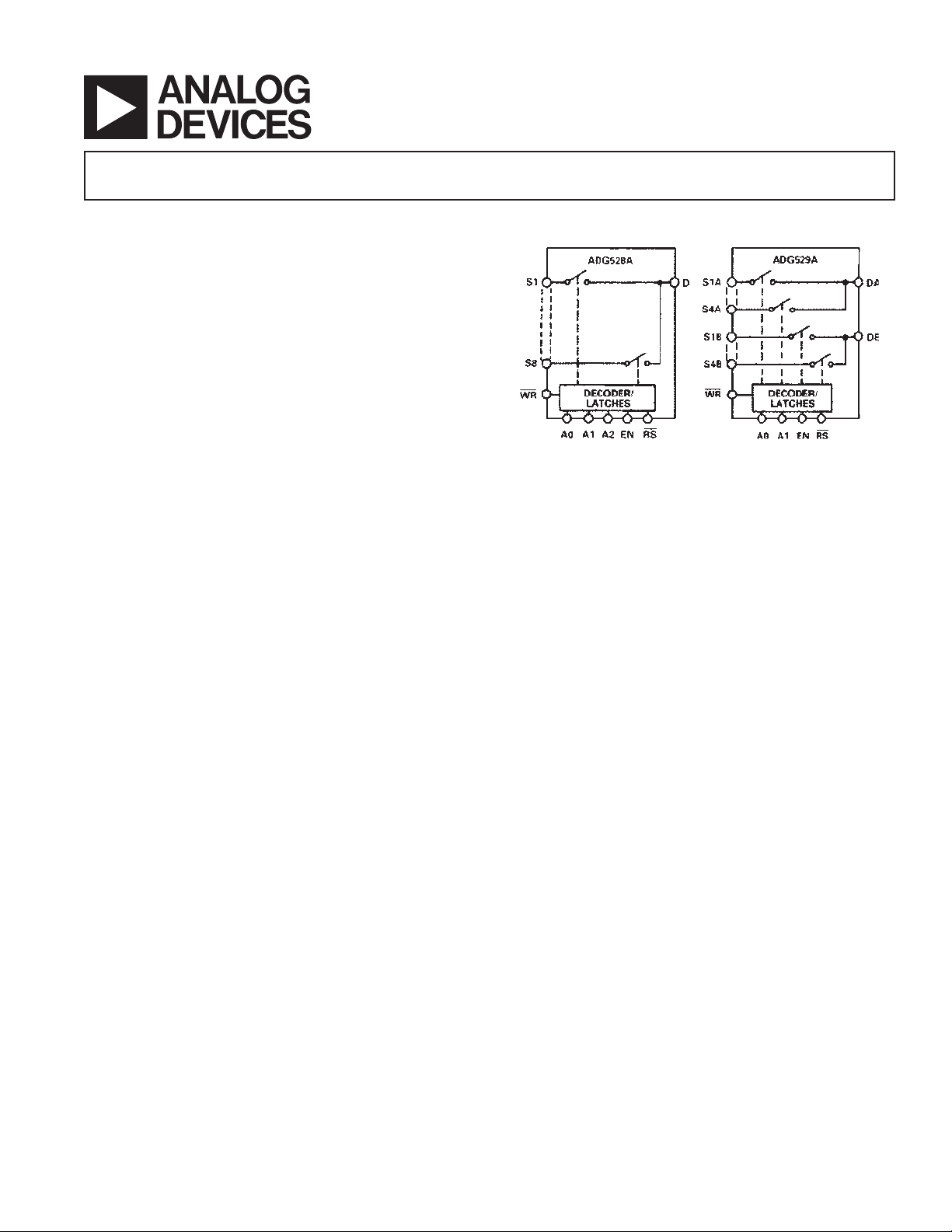
GENERAL DESCRIPTION
The ADG528A and ADG529A are CMOS monolithic analog
multiplexers with eight channels and four dual channels, respectively. On-chip latches facilitate microprocessor interfacing. The
ADG528A switches one of eight inputs to a common output,
depending on the state of three binary addresses and an enable
input. The ADG529A switches one of four differential inputs to
a common differential output, depending on the state of two
binary addresses and an enable input. Both devices have TTL
and 5 V CMOS logic-compatible digital inputs.
The ADG528A and ADG529A are designed on an enhanced
LC2MOS process, which gives an increased signal capability of
to VDD and enables operation over a wide range of supply
V
SS
voltages. The devices can comfortably operate anywhere in the
10.8 V to 16.5 V single- or dual-supply range. These multiplexers also feature high switching and low R
ON
.
FUNCTIONAL BLOCK DIAGRAMS
PRODUCT HIGHLIGHTS
1. Single-/dual-supply specifications with a wide tolerance.
The devices are specified in the 10.8 V to 16.5 V range for
both single- and dual-supplies.
2. Easily Interfaced
The ADG528A and ADG529A can be easily interfaced with
microprocessors. The WR signal latches the state of the
address control lines and the enable line. The RS signal
clears both the address and enable data in the latches resulting in no output (all switches off). RS can be tied to the
microprocessor reset pin.
3. Extended Signal Range
The enhanced LC
and an increased analog signal range of V
4. Break-Before-Make Switching
Switches are guaranteed break-before-make so that input
signals are protected against momentary shorting.
5. Low Leakage
Leakage currents in the range of 20 pA make these multiplexers
suitable for high precision circuits.
2
MOS processing results in a high breakdown
to VDD.
SS
REV. B
Information furnished by Analog Devices is believed to be accurate and
reliable. However, no responsibility is assumed by Analog Devices for its
use, nor for any infringements of patents or other rights of third parties that
may result from its use. No license is granted by implication or otherwise
under any patent or patent rights of Analog Devices. Trademarks and
registered trademarks are the property of their respective owners.
One Technology Way, P.O. Box 9106, Norwood, MA 02062-9106, U.S.A.
Tel: 781/329-4700 www.analog.com
Fax: 781/326-8703 © 2004 Analog Devices, Inc. All rights reserved.
Page 2

ADG528A/ADG529A–SPECIFICATIONS
DUAL SUPPLY
(VDD = +10.8 V to +16.5 V, VSS = –10.8 V to –16.5 V, unless otherwise noted.)
ADG528A ADG528A ADG528A
ADG529A ADG529A ADG529A
K Version B Version T Version
–40°C to –40°C to –55°C to
Parameter +25°C +85°C +25°C +85°C +25°C +125°C Units Comments
ANALOG SWITCH
Analog Signal Range V
R
ON
SS
V
DDVDD
V
SS
V
SS
V
DDVDD
V
SS
V
SS
V
DDVDD
V
SS
V min
V max
280 280 280 Ω typ –10 V ≤ VS ≤ +10 V, IDS = 1 mA;
Test Circuit 1
450 600 450 600 450 600 Ω max
300 400 300 400 Ω max V
300 400 Ω max V
Drift 0.6 0.6 0.6 %/°C typ –10 V ≤ VS ≤ +10 V, IDS = 1 mA
R
ON
R
Match 5 5 5 % typ –10 V ≤ VS ≤ +10 V, IDS = 1 mA
ON
I
(OFF), Off Input
S
= 15 V (±10%), VSS = –15 V (± 10%)
DD
= 15 V (± 5%), VSS = –15 V (± 5%)
DD
Leakage 0.02 0.02 0.02 nA typ V1 = ±10 V, V2 = ⫿10 V; Test Circuit 2
150 150 150 nA max
I
(OFF), Off Input
D
Leakage 0.04 0.04 0.04 nA typ V1 = ±10 V, V2 = ⫿10 V; Test Circuit 3
ADG528A 1 100 1 100 1 100 nA max
ADG529A 1 50 1 50 1 50 nA max
ID (ON), On Channel
Leakage 0.04 0.04 0.04 nA typ V1 = ±10 V, V2 = ⫿10 V; Test Circuit 4
ADG528A 1 100 1 100 1 100 nA max
ADG529A 1 50 1 50 1 50 nA max
I
, Differential Off
DIFF
Output Leakage
(ADG529A only) 25 25 25 nA max V1 = ±10 V, V2 = ⫿10 V; Test Circuit 5
DIGITAL CONTROL
V
, Input High Voltage 2.4 2.4 2.4 V min
INH
, Input Low Voltage 0.8 0.8 0.8 V max
V
INL
I
INL
or I
INH
111µA max VIN = 0 to V
DD
CIN Digital Input
Capacitance 8 8 8 pF max
DYNAMIC CHARACTERISTICS
t
TRANSITION
1
200 200 200 ns typ V1 = ± 10 V, V2 = ⫿10 V; Test Circuit 6
300 400 300 400 300 400 ns max
t
OPEN
50 50 50 ns typ Test Circuit 7
25 10 25 10 25 10 ns min
tON (EN, WR) 200 200 200 ns typ Test Circuits 8 and 9
300 400 300 400 300 400 ns max
t
(EN, RS) 200 200 200 ns typ Test Circuits 8 and 10
OFF
300 400 300 400 300 400 ns max
tW Write Pulse Width 100 120 100 120 100 130 ns min See Figure 1
t
Address,
S
Enable Setup Time 100 100 100 ns min See Figure 1
tH, Address,
Enable Hold Time 10 10 10 ns min See Figure 1
tRS Reset Pulse Width 100 100 100 ns min See Figure 2
OFF Isolation 68 68 68 dB typ V
50 50 50 dB min V
(OFF) 5 5 5 pF typ VEN = 0.8 V
C
S
C
(OFF)
D
ADG528A 22 22 22 pF typ V
= 0.8 V, RL = 1 kΩ, CL = 15 pF,
EN
= 7 V rms, f = 100 kHz
S
= 0.8 V
EN
ADG529A 11 11 11 pF typ
Q
, Charge Injection 4 4 4 pC typ RS = 0 Ω, VS = 0 V; Test Circuit 11
INJ
REV. B–2–
Page 3
ADG528A/ADG529A
ADG528A ADG528A ADG528A
ADG529A ADG529A ADG529A
K Version B Version T Version
–40°C to –40°C to –55°C to
Parameter +25°C +85°C +25°C +85°C +25°C +125°CUnits Comments
POWER SUPPLY
I
DD
I
SS
Power Dissipation 10 10 10 mW typ
NOTE
1
Sample tested at +25°C to ensure compliance.
Specifications subject to change without notice.
0.6 0.6 0.6 mA typ VIN = V
1.5 1.5 1.5 mA max
20 20 20 µA typ VIN = V
0.2 0.2 0.2 mA max
2.8 2.8 2.8 mW max
INL
INL
or V
or V
INH
INH
SINGLE SUPPLY
(VDD = +10.8 V to +16.5 V, VSS = GND = 0 V, unless otherwise noted.)
ADG528A ADG528A ADG528A
ADG529A ADG529A ADG529A
K Version B Version T Version
–40°C to –40°C to –55°C to
Parameter +25°C +85°C +25°C +85°C +25°C +125°CUnits Comments
ANALOG SWITCH
Analog Signal Range GND GND GND GND GND GND V min
V
R
ON
DDVDD
V
DDVDD
V
DDVDD
V max
500 500 500 Ω typ GND ≤ VS ≤ +10 V, IDS = 0.5 mA;
Test Circuit 1
700 1000 700 1000 700 1000 Ω max
R
Drift 0.6 0.6 0.6 %/°C typ GND ≤ VS ≤ +10 V, IDS = 0.5 mA
ON
R
Match 5 5 5 % typ GND ≤ VS ≤ +10 V, IDS = 0.5 mA
ON
(OFF), Off Input
I
S
Leakage 0.02 0.02 0.02 nA typ V1 = +10 V/GND, V2 = GND/+10 V;
150150 1 50 nA max Test Circuit 2
I
(OFF), Off Input
D
Leakage 0.04 0.04 0.04 nA typ V1 = +10 V/GND, V2 = GND/+10 V;
ADG528A 1 100 1 100 1 100 nA max Test Circuit 3
ADG529A 1 50 1 50 1 50 nA max
I
(ON), On Channel
D
Leakage 0.04 0.04 0.04 nA typ V1 = +10 V/GND, V2 = GND/+10 V;
ADG528A 1 100 1 100 1 100 nA max Test Circuit 4
ADG529A 1 50 1 50 1 50 nA max
I
, Differential Off
DIFF
Output Leakage
(ADG529A only) 25 25 25 nA max V1 = +10 V/GND, V2 = GND/+10 V;
Test Circuit 5
DIGITAL CONTROL
V
, Input High Voltage 2.4 2.4 2.4 V min
INH
V
, Input Low Voltage 0.8 0.8 0.8 V max
INL
I
INL
or I
INH
111µA max VIN = 0 to V
DD
CIN Digital Input
Capacitance 8 8 8 pF max
DYNAMIC CHARACTERISTICS
t
TRANSITION
1
300 300 300 ns typ V1 = +10 V/GND, V2 = GND/+10 V;
Test Circuit 6
450 600 450 600 450 600 ns max
t
OPEN
50 50 50 ns typ Test Circuit 7
25 10 25 10 25 10 ns min
t
(EN, WR) 250 250 250 ns typ Test Circuits 8 and 9
ON
450 600 450 600 450 600 ns max
t
(EN, RS) 250 250 250 ns typ Test Circuits 8 and 10
OFF
450 600 450 600 450 600 ns max
tW Write Pulse Width 100 120 100 120 100 130 ns min See Figure 1
REV. B
–3–
Page 4

ADG528A/ADG529A
ADG528A ADG528A ADG528A
ADG529A ADG529A ADG529A
K Version B Version T Version
–40°C to –40°C to –55°C to
Parameter +25°C +85°C +25°C +85°C +25°C +125°C Units Comments
DYNAMIC CHARACTERISTICS1 (Cont’d)
t
Address,
S
Enable Setup Time 100 100 100 ns min See Figure 1
t
Address,
H
Enable Hold Time 10 10 10 ns min See Figure 1
tRS Reset Pulse Width 100 100 100 ns min See Figure 2
OFF Isolation 68 68 68 dB typ V
50 50 50 dB min V
(OFF) 5 5 5 pF typ VEN = 0.8 V
C
S
C
(OFF)
D
ADG528A 22 22 22 pF typ V
ADG529A 11 11 11 pF typ
Q
, Charge Injection 4 4 4 pC typ RS = 0 Ω, VS = 0 V; Test Circuit 11
INJ
POWER SUPPLY
I
DD
0.6 0.6 0.6 mA typ VIN = V
1.5 1.5 1.5 mA max
Power Dissipation 11 10 10 mW typ
25 25 25 mW max
NOTE
1
Sample tested at +25°C to ensure compliance.
Specifications subject to change without notice.
= 0.8 V, RL = 1 kΩ, CL = 15 pF,
EN
= 3.5 V rms, f = 100 kHz
S
= 0.8 V
EN
or V
INL
INH
REV. B–4–
Page 5

ADG528A/ADG529A
PIN CONFIGURATIONS
PLCCDIP/SOIC
ABSOLUTE MAXIMUM RATINGS
1
(TA = +25°C, unless otherwise noted)
to VSS . . . . . . . . . . . . . . . . . . . . . . . . . . . . . . . . . . . . . 44 V
V
DD
V
to GND . . . . . . . . . . . . . . . . . . . . . . . . . . . . . . . . . . . 25 V
DD
to GND . . . . . . . . . . . . . . . . . . . . . . . . . . . . . . . . . . . –25 V
V
SS
Analog Inputs
2
Voltage at S, D . . . . . . . . . VSS – 2 V to VDD + 2 V or 20 mA,
whichever Occurs First
Continuous Current, S or D . . . . . . . . . . . . . . . . . . . 20 mA
Pulsed Current, S or D
1 ms duration, 10% Duty Cycle . . . . . . . . . . . . . . . 40 mA
Digital Inputs
1
Voltage at A, EN, WR, RS . . . . . . VSS – 4 V to VDD + 4 V or
20 mA, whichever Occurs First
Power Dissipation (Any Package)
Up to +75°C . . . . . . . . . . . . . . . . . . . . . . . . . . . . . . 470 mW
Derates above +75°C . . . . . . . . . . . . . . . . . . . . . . . 6 mW/°C
Operating Temperature
Commercial (K Version) . . . . . . . . . . . . . . .–40°C to +85°C
Industrial (B Version) . . . . . . . . . . . . . . . . .–40°C to +85°C
Extended (T Version) . . . . . . . . . . . . . . . .–55°C to +125°C
Storage Temperature Range . . . . . . . . . . . . .–65°C to +150°C
Lead Temperature (Soldering, 10 sec) . . . . . . . . . . . . +300°C
NOTES
1
Stresses above those listed under “Absolute Maximum Ratings” may cause permanent
damage to the device. This is a stress rating only and functional operation of the device
at these or any other conditions above those indicated in the operational sections of this
specification is not implied. Exposure to absolute maximum rating conditions for
extended periods may affect device reliability.
2
Overvoltage at A, EN, WR, RS, S or D will be clamped by diodes. Current should
be limited to the maximum rating above.
ORDERING GUIDE
Temperature Package Package
Model Range Description Option
ADG528AKN –40°C to +85°C PDIP N-18
ADG528AKP –40°C to +85°C PLCC P-20A
ADG528AKP-REEL –40°C to +85°C PLCC P-20A
ADG528ABQ –40°C to +85°C CERDIP Q-18
ADG528ATQ –55°C to +125°C CERDIP Q-18
ADG528ABCHIPS DIE
ADG528ATCHIPS DIE
ADG529AKN –40°C to +85°C PDIP N-18
ADG529AKP –40°C to +85°C PLCC P-20A
ADG529AKRW –40°C to +85°C SOIC RW-18
ADG529AKRW-REEL –40°C to +85°C SOIC RW-18
ADG529AKRW-REEL7 –40°C to +85°C SOIC RW-18
ADG529ABQ –40°C to +85°C CERDIP Q-18
ADG529ATQ –55°C to +125°C CERDIP Q-18
ADG529ABCHIPS DIE
ADG529ATCHIPS DIE
NOTES
1
N = Plastic DIP; P = Plastic Leaded Chip Carrier (PLCC); Q = Cerdip; RW = SOIC.
CAUTION
ESD (electrostatic discharge) sensitive device. Electrostatic charges as high as 4000 V readily
accumulate on the human body and test equipment and can discharge without detection. Although the
WARNING!
ADG528A/ADG529A features proprietary ESD protection circuitry, permanent damage may occur
on devices subjected to high energy electrostatic discharges. Therefore, proper ESD precautions are
recommended to avoid performance degradation or loss of functionality.
1
ESD SENSITIVE DEVICE
REV. B
–5–
Page 6

ADG528A/ADG529A
TRUTH TABLES
A2 A1 A0 EN WR RS ON SWITCH PAIR
XXXX
1Retains Previous Switch Condition
XXXX X 0 NONE (Address and Enable
Latches Cleared)
XXX0 0 1 NONE
0001 0 11
0011 0 12
0101 0 13
0111 0 14
1001 0 15
1011 0 16
1101 0 17
1111 0 18
X = Don’t Care ADG528A
A1 A0 EN WR RS ON SWITCH PAIR
XXX
1Retains Previous Switch Condition
XXX X0NONE (Address and Enable Latches
Cleared)
XX0 01NONE
001 0 11
011 0 12
101 0 13
111 0 14
X = Don’t Care ADG529A
TIMING DIAGRAMS
Figure 1.
Figure 2.
Figure 1 shows the timing sequence for latching the switch
address and enable inputs. The latches are level sensitive; therefore, while WR is held low, the latches are transparent and the
switches respond to the address and enable inputs. This input
data is latched on the rising edge of WR.
Figure 2 shows the Reset Pulse Width, t
Time, t
OFF
(RS).
, and Reset Turn-off
RS
Note: All digital input signals rise and fall times measured from
10% to 90% of 3 V. t
= tF = 20 ns.
R
REV. B–6–
Page 7

Typical Performance Characteristics–ADG528A/ADG529A
The multiplexers are guaranteed functional with reduced single or dual supplies down to 4.5 V.
TPC 1. RON as a Function of VD(VS): Dual Supply
Voltage, T
TPC 2. Leakage Current as a Function of Temperature
(Note: Leakage Currents Reduce as the Supply
Voltages Reduce)
= +25°C
A
TPC 4. Trigger Levels vs. Power Supply Voltage,
Dual or Single Supply, TA = +25°C
TPC 5. t
Single Supplies, TA = +25°C
(Note: For VDD and |VSS| < 10 V; V1 = VDD/VSS, V2 =
V
TRANSITION
. See Test Circuit 6)
SS/VDD
vs. Supply Voltage: Dual and
TPC 3. RON as a Function of VD(VS): Single Supply
Voltage, TA = +25°C
REV. B
TPC 6. IDD vs. Supply Voltage: Dual or Single
Supply, TA = +25°C
–7–
Page 8

ADG528A/ADG529A
Test Circuits
Test Circuit 1. R
Test Circuit 2. IS (OFF)
Test Circuit 3. ID (OFF)
ON
Test Circuit 4. ID (ON)
Test Circuit 5. I
Test Circuit 6. Switching Time of Multiplexer, t
DIFF
TRANSITION
Test Circuit 7. Break-Before-Make Delay, t
OPEN
REV. B–8–
Page 9

ADG528A/ADG529A
Test Circuit 8. Enable Delay, tON (EN), t
Test Circuit 9. Write Turn-On Time, tON (WR)
OFF
(EN)
REV. B
Test Circuit 10. Reset Turn-Off Time, t
Test Circuit 11. Charge Injection
–9–
OFF
(RS)
Page 10

ADG528A/ADG529A
TERMINOLOGY
R
ON
RON Match Difference between the RON of any two channels
RON Drift Change in RON versus temperature
(OFF) Source terminal leakage current when the switch
I
S
I
(OFF) Drain terminal leakage current when the switch is
D
ID (ON) Leakage current that flows from the closed switch
VS (VD)Analog voltage on terminal S or D
CS (OFF) Channel input capacitance for “OFF” condition
CD (OFF) Channel output capacitance for “OFF” condition
C
IN
tON (EN) Delay time between the 50% and 90% points of
Ohmic resistance between terminals D and S
is off.
off.
into the body.
Digital input capacitance
the digital input and switch “ON” condition.
OUTLINE DIMENSIONS
18-Lead Plastic Dual In-Line Package [PDIP]
(N-18)
Dimensions shown in inches and (millimeters)
t
(EN) Delay time between the 50% and 10% points of
OFF
the digital input and switch “OFF” condition
t
TRANSITION
Delay time between the 50% and 90% points of
the digital inputs and switch “ON” condition
when switching from one address state to another.
t
OPEN
“OFF” time measured between 50% points of
both switches when switching from one address
state to another
V
V
I
V
V
I
I
INL
INH
INL
DD
SS
DD
SS
(I
Maximum input voltage for Logic “0”
Minimum input voltage for Logic “1”
) Input current of the digital input
INH
Most positive voltage supply
Most negative voltage supply
Positive supply current
Negative supply current
0.048 (1.21)
0.042 (1.07)
0.885 (22.48)
0.845 (21.46)
18
1
0.180 (4.57)
MAX
0.150 (3.81)
0.110 (2.79)
0.022 (0.558)
0.014 (0.356)
CONTROLLING DIMENSIONS ARE IN INCHES; MILLIMETER DIMENSIONS
(IN PARENTHESES) ARE ROUNDED-OFF INCH EQUIVALENTS FOR
REFERENCE ONLY AND ARE NOT APPROPRIATE FOR USE IN DESIGN
0.015 (0.38) MIN
0.100
0.060 (1.52)
(2.54)
0.045 (1.14)
BSC
COMPLIANT TO JEDEC STANDARDS MO-095AD
0.295 (7.49)
0.275 (6.99)
10
9
SEATING
PLANE
0.325 (8.26)
0.300 (7.62)
20-Lead Plastic Leaded Chip Carrier [PLCC]
(P-20A)
Dimensions shown in inches and (millimeters)
0.048 (1.21)
0.042 (1.07)
3
4
TOP VIEW
(PINS DOWN)
8
0.020
(0.50)
9
0.356 (9.04)
R
0.350 (8.89)
0.395 (10.02)
0.385 (9.78)
CONTROLLING DIMENSIONS ARE IN INCHES; MILLIMETER DIMENSIONS
(IN PARENTHESES) ARE ROUNDED-OFF INCH EQUIVALENTS FOR
REFERENCE ONLY AND ARE NOT APPROPRIATE FOR USE IN DESIGN
0.056 (1.42)
0.042 (1.07)
19
18
0.050
(1.27)
BSC
14
13
SQ
SQ
COMPLIANT TO JEDEC STANDARDS MO-047AA
0.180 (4.57)
0.165 (4.19)
0.120 (3.04)
0.090 (2.29)
0.20 (0.51)
MIN
0.021 (0.53)
0.013 (0.33)
0.032 (0.81)
0.026 (0.66)
0.040 (1.01)
0.025 (0.64)
0.015 (0.381)
0.008 (0.203)
0.330 (8.38)
0.290 (7.37)
R
0.180 (4.57)
MAX
0.020 (0.50)
R
BOTTOM
VIEW
(PINS UP)
REV. B–10–
Page 11

OUTLINE DIMENSIONS
18-Lead Ceramic Dual In-Line Package [CERDIP]
(Q-18)
Dimensions shown in inches and (millimeters)
ADG528A/ADG529A
0.005
(0.13)
MIN
PIN 1
0.200
(5.08)
MAX
0.200 (5.08)
0.125 (3.18)
0.023 (0.58)
0.014 (0.36)
CONTROLLING DIMENSIONS ARE IN INCHES; MILLIMETER DIMENSIONS
(IN PARENTHESES) ARE ROUNDED-OFF INCH EQUIVALENTS FOR
REFERENCE ONLY AND ARE NOT APPROPRIATE FOR USE IN DESIGN
0.098 (2.49)
MAX
18
19
0.960 (24.38) MAX
0.100
0.070 (1.78)
(2.54)
0.030 (0.76)
BSC
10
0.310 (7.87)
0.220 (5.59)
0.060 (1.52)
0.015 (0.38)
0.150 (3.81)
MIN
SEATING
PLANE
18-Lead Standard Small Outline Package [SOIC]
Wide Body
(RW-18)
Dimensions shown in millimeters and (inches)
11.75 (0.4626)
11.35 (0.4469)
18 10
1
7.60 (0.2992)
7.40 (0.2913)
9
10.65 (0.4193)
10.00 (0.3937)
15
0
0.320 (8.13)
0.290 (7.37)
0.015 (0.38)
0.008 (0.20)
2.65 (0.1043)
0.30 (0.0118)
0.10 (0.0039)
COPLANARITY
0.10
CONTROLLING DIMENSIONS ARE IN MILLIMETERS; INCH DIMENSIONS
(IN PARENTHESES) ARE ROUNDED-OFF MILLIMETER EQUIVALENTS FOR
REFERENCE ONLY AND ARE NOT APPROPRIATE FOR USE IN DESIGN
1.27
(0.0500)
BSC
0.51 (0.0201)
0.31 (0.0122)
COMPLIANT TO JEDEC STANDARDS MS-013AB
2.35 (0.0925)
SEATING
PLANE
0.33 (0.0130)
0.20 (0.0079)
0.75 (0.0295)
0.25 (0.0098)
8ⴗ
0ⴗ
ⴛ 45ⴗ
1.27 (0.0500)
0.40 (0.0157)
REV. B
–11–
Page 12

ADG528A/ADG529A
Revision History
Location Page
10/04—Data Sheet Changed from Rev. A to Rev. B
Deleted 20-Lead LCC package . . . . . . . . . . . . . . . . . . . . . . . . . . . . . . . . . . . . . . . . . . . . . . . . . . . . . . . . . . . . . . . . . . . . . . .Universal
Changes to FEATURES . . . . . . . . . . . . . . . . . . . . . . . . . . . . . . . . . . . . . . . . . . . . . . . . . . . . . . . . . . . . . . . . . . . . . . . . . . . . . . . . . . 5
Changes to ORDERING GUIDE . . . . . . . . . . . . . . . . . . . . . . . . . . . . . . . . . . . . . . . . . . . . . . . . . . . . . . . . . . . . . . . . . . . . . . . . . . . 6
SOIC added to DIP PIN CONFIGURATION . . . . . . . . . . . . . . . . . . . . . . . . . . . . . . . . . . . . . . . . . . . . . . . . . . . . . . . . . . . . . . . . . 5
Updated OUTLINE DIMENSIONS . . . . . . . . . . . . . . . . . . . . . . . . . . . . . . . . . . . . . . . . . . . . . . . . . . . . . . . . . . . . . . . . . . . . . . . . 9
C03337–0–10/04(B)
–12–
REV. B
 Loading...