

Page 1
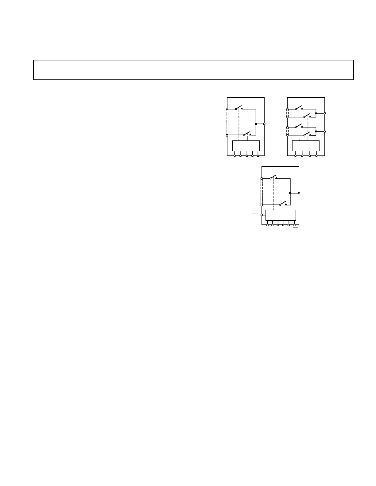
a
ADG407
ENA0 A1 A2
S1A
S8A
DA
S8B
DB
S1B
1 OF 8
DECODER
ENA0 A1 A2 A3 RS
ADG426
S1
S16
D
WR
DECODER/
LATCHES
ADG406
ENA0 A1 A2 A3
S1
S16
D
1 OF 16
DECODER
LC2MOS 8-/16-Channel
High Performance Analog Multiplexers
ADG406/ADG407/ADG426
FEATURES
44 V Supply Maximum Ratings
VSS to VDD Analog Signal Range
Low On Resistance (80 Ω max)
Low Power
Fast Switching
< 160 ns
t
ON
t
< 150 ns
OFF
Break Before Make Switching Action
Plug-In Upgrade for
DG506A/ADG506A, DG507A/ADG507A,
DG526/ADG526A
ADG406/ADG407 are Plug-In Replacements for
DG406/DG407
APPLICATIONS
Audio and Video Routing
Automatic Test Equipment
Data Acquisition Systems
Battery Powered Systems
Sample Hold Systems
Communication Systems
Avionics
GENERAL DESCRIPTION
The ADG406, ADG407 and ADG426 are monolithic CMOS
analog multiplexers. The ADG406 and ADG426 switch one of
sixteen inputs to a common output as determined by the 4-bit
binary address lines A0, A1, A2 and A3. The ADG426 has onchip address and control latches that facilitate microprocessor
interfacing. The ADG407 switches one of eight differential
inputs to a common differential output as determined by the 3bit binary address lines A0, A1 and A2. An EN input on all
devices is used to enable or disable the device. When disabled,
all channels are switched OFF.
The ADG406/ADG407/ADG426 are designed on an enhanced
2
LC
MOS process that provides low power dissipation yet gives
high switching speed and low on resistance. These features
make the parts suitable for high speed data acquisition systems
and audio signal switching. Low power dissipation makes the
parts suitable for battery powered systems. Each channel
conducts equally well in both directions when ON and has an
input signal range which extends to the supplies. In the OFF
condition, signal levels up to the supplies are blocked. All
channels exhibit break before make switching action preventing
momentary shorting when switching channels. Inherent in the
design is low charge injection for minimum transients when
switching the digital inputs.
FUNCTIONAL BLOCK DIAGRAMS
PRODUCT HIGHLIGHTS
1. Extended Signal Range
The ADG406/ADG407/ADG426 are fabricated on an
enhanced LC
2
MOS process giving an increased signal range
which extends to the supply rails
2. Low Power Dissipation
3. Low R
ON
4. Single/Dual Supply Operation
5. Single Supply Operation
For applications where the analog signal is unipolar, the
ADG406/ADG407/ADG426 can be operated from a single
rail power supply. The parts are fully specified with a single
+12 V power supply and will remain functional with single
supplies as low as +5 V.
REV. 0
Information furnished by Analog Devices is believed to be accurate and
reliable. However, no responsibility is assumed by Analog Devices for its
use, nor for any infringements of patents or other rights of third parties
which may result from its use. No license is granted by implication or
otherwise under any patent or patent rights of Analog Devices.
One Technology Way, P.O. Box 9106, Norwood. MA 02062-9106, U.S.A.
Tel: 617/329-4700 Fax: 617/326-8703
Page 2

1
ADG406/ADG407/ADG426–SPECIFICATIONS
(V
= +15 V ± 10%, V
DUAL SUPPLY
DD
B Version T Version
Parameter +25°C +85°C +25°C +125°C Units Test Conditions/Comments
ANALOG SWITCH
Analog Signal Range VSS to V
R
ON
R
Match 4 4 Ω typ VD = 0 V, IS = –1 mA
ON
50 50 Ω typ VD = ±10 V, IS = –1 mA
80 125 80 125 Ω max VDD = +13.5 V, VSS = –13.5 V
LEAKAGE CURRENTS VDD = +16.5 V, VSS = –16.5 V
Source OFF Leakage IS (OFF) ± 0.5 ±20 ±0.5 ±50 nA max VD = ±10 V, VS = 710 V, Test Circuit 2
Drain OFF Leakage ID (OFF) VD = ±10 V, VS = 710 V;
ADG406, ADG426 ±1 ±20 ±1 ±200 nA max Test Circuit 3
ADG407 ±1 ±20 ±1 ±100 nA max
Channel ON Leakage ID, IS (ON) VS = VD = ±10 V;
ADG406, ADG426 ± 1 ± 20 ±1 ±200 nA max Test Circuit 4
ADG407 ±1 ±20 ±1 ±100 nA max
DIGITAL INPUTS
Input High Voltage, V
Input Low Voltage, V
Input Current
I
or I
INL
CIN, Digital Input Capacitance 8 8 pF typ f = 1 MHz
INH
DYNAMIC CHARACTERISTICS
t
TRANSITION
Break Before Make Delay, t
t
(EN, WR) 120 175 120 175 ns typ RL = 300 Ω, CL = 35 pF;
ON
t
(EN, RS) 110 130 110 130 ns typ RL = 300 Ω, CL = 35 pF;
OFF
INL
INH
OPEN
2
120 120 ns typ RL = 300 Ω, CL = 35 pF;
150 250 150 250 ns max V1 = ±10 V, V2 = 710 V;
10 10 10 10 ns min RL = 300 Ω, CL = 35 pF;
160 225 160 225 ns max VS = +5 V, Test Circuit 7
150 180 150 180 ns max VS = +5 V, Test Circuit 7
ADG426 Only
tW, Write Pulse Width 100 100 ns min
tS, Address, Enable Setup Time 100 100 ns min
tH, Address, Enable Hold Time 10 10 ns min
tRS, Reset Pulse Width 100 100 ns min VS = +5 V
Charge Injection 8 8 pC typ VS = 0 V, RS = 0 Ω, CL = 1 nF;
OFF Isolation –75 –75 dB typ RL = 1 kΩ, f = 100 kHz;
Channel-to-Channel Crosstalk 85 85 dB typ RL = 1 kΩ, f = 100 kHz, Test Circuit 12
CS (OFF) 5 5 pF typ f = 1 MHz
CD (OFF) f = 1 MHz
ADG406, ADG426 50 50 pF typ
ADG407 25 25 pF typ
CD, CS (ON) f = 1 MHz
ADG406, ADG426 60 60 pF typ
ADG407 40 40 pF typ
= –15 V ± 10%, GND = 0 V, unless otherwise noted)
SS
–40°C to –55°C to
DD
VSS to VDDV
2.4 2.4 V min
0.8 0.8 V max
±1 ±1 µA max VIN = 0 or V
Test Circuit 5
VS = +5 V, Test Circuit 6
Test Circuit 10
VEN = 0 V, Test Circuit 11
DD
POWER REQUIREMENTS VDD = +16.5 V, VSS = –16.5 V
I
DD
I
SS
I
DD
I
SS
N
OTES
1
Temperature ranges are as follows: B Versions: –40°C to +85°C; T Versions: –55°C to +125°C.
2
Guaranteed by design, not subject to production test.
Specifications subject to change without notice.
100 100 µA typ VIN = 0 V, VEN = 2.4 V
200 500 200 500 µA max
11µA typ VIN = 0 V, VEN = 0 V
55µA max
11µA typ
55µA max
11µA typ
55µA max
–2–
REV. 0
Page 3
SINGLE SUPPLY
(V
= +12 V ± 10%, V
DD
= 0 V, GND = 0 V, unless otherwise noted)
SS
ADG406/ADG407/ADG426
B Version T Version
–40°C to –55°C to
Parameter +25°C +85°C +25°C +125°C Units Test Conditions/Comments
ANALOG SWITCH
Analog Signal Range 0 to V
R
ON
90 90 Ω typ VD = +3 V, +8.5 V, IS = –1 mA;
125 200 125 200 Ω max VDD = +10.8 V
DD
0 to V
DD
V
LEAKAGE CURRENTS VDD = +13.2 V
Source OFF Leakage IS (OFF) ±0.5 ±20 ±0.5 ±50 nA max VD = 8 V/0.1 V, VS = 0.1 V/8 V;
Test Circuit 2
Drain OFF Leakage ID (OFF) VD = 8 V/0.1 V, VS = 0.1 V/8 V;
ADG406, ADG426 ± 1 ± 20 ±1 ±200 nA max Test Circuit 3
ADG407 ±1 ±20 ±1 ±100 nA max
Channel ON Leakage ID, IS (ON) VS = VD = 8 V/0.1 V, Test Circuit 4
ADG406, ADG426 ± 1 ± 20 ±1 ±200 nA max
ADG407 ±1 ±20 ±1 ±100 nA max
DIGITAL INPUTS
Input High Voltage, V
Input Low Voltage, V
Input Current
I
or I
INL
CIN, Digital Input Capacitance 8 8 pF typ f = 1 MHz
INH
DYNAMIC CHARACTERISTICS
t
TRANSITION
INH
INL
2
180 180 ns typ RL = 300 Ω, CL = 35 pF;
220 350 220 350 ns max V1 = 8 V/0 V, V2 = 0 V/8 V;
2.4 2.4 V min
0.8 0.8 V max
±1 ±1 µA max VIN = 0 or V
DD
Test Circuit 5
Break Before Make Delay, t
t
(EN, WR) 180 180 ns typ RL = 300 Ω, CL = 35 pF;
ON
t
(EN, RS) 135 135 ns typ RL = 300 Ω, CL = 35 pF;
OFF
OPEN
10 10 ns typ RL = 300 Ω, CL = 35 pF;
VS = +5 V, Test Circuit 6
240 350 240 350 ns max VS = +5 V, Test Circuit 7
180 220 180 220 ns max VS = +5 V, Test Circuit 7
ADG426 Only
tW, Write Pulse Width 100 100 ns min
tS, Address, Enable Setup Time 100 100 ns min
tH, Address, Enable Hold Time 10 10 ns min
tRS, Reset Pulse Width 100 100 ns min VS = +5 V
Charge Injection 5 5 pC typ VS = 6 V, RS = 0 Ω, CL = 1 nF;
Test Circuit 10
OFF Isolation –75 –75 dB typ RL = 1 kΩ, f = 100 kHz;
Test Circuit 11
Channel-to-Channel Crosstalk 85 85 dB typ RL = 1 kΩ, f = 100 kHz;
Test Circuit 12
CS (OFF) 8 8 pF typ f = 1 MHz
CD (OFF) f = 1 MHz
ADG406, ADG426 80 80 pF typ
ADG407 40 40 pF typ
CD, CS (ON) f = 1 MHz
ADG406, ADG426 100 100 pF typ
ADG407 50 50 pF typ
POWER REQUIREMENTS VDD = +13.2 V
I
DD
I
DD
NOTES
1
Temperature ranges are as follows: B Versions: –40°C to +85°C; T Versions: –55°C to +125°C.
2
Guaranteed by design, not subject to production test.
Specifications subject to change without notice.
100 100 µA typ VIN = 0 V, VEN = 2.4 V
200 500 200 500 µA max
REV. 0
11µA typ VIN = 0 V, VEN = 0 V
55µA max
–3–
Page 4
ADG406/ADG407/ADG426
ABSOLUTE MAXIMUM RATINGS
(TA = +25°C unless otherwise noted)
1
VDD to VSS . . . . . . . . . . . . . . . . . . . . . . . . . . . . . . . . . . . .+44 V
V
to GND . . . . . . . . . . . . . . . . . . . . . . . . . . –0.3 V to +25 V
DD
V
to GND . . . . . . . . . . . . . . . . . . . . . . . . . . . +0.3 V to –25 V
SS
Analog, Digital Inputs
2
. . . . . . . . . . . . . VSS – 2 V to VDD + 2 V
or 20 mA, Whichever Occurs First
Continuous Current, S or D . . . . . . . . . . . . . . . . . . . . . 20 mA
Peak Current, S or D . . . . . . . . . . . . . . . . . . . . . . . . . . . 40 mA
(Pulsed at 1 ms, 10% Duty Cycle Max)
Operating Temperature Range
Industrial (B Version) . . . . . . . . . . . . . . . . . –40°C to +85°C
Extended (T Version) . . . . . . . . . . . . . . . . .–55°C to +125°C
Storage Temperature Range . . . . . . . . . . . . . –65°C to +150°C
Junction Temperature . . . . . . . . . . . . . . . . . . . . . . . . . +150°C
Plastic Package
θ
, Thermal Impedance . . . . . . . . . . . . . . . . . . . . . . 75°C/W
JA
Lead Temperature, Soldering (10 sec) . . . . . . . . . . . +260°C
PLCC Package
θ
, Thermal Impedance . . . . . . . . . . . . . . . . . . . . . . 80°C/W
JA
Lead Temperature, Soldering
Vapor Phase (60 sec) . . . . . . . . . . . . . . . . . . . . . . +215°C
Infrared (15 sec) . . . . . . . . . . . . . . . . . . . . . . . . . . +220°C
SSOP Package
θ
, Thermal Impedance . . . . . . . . . . . . . . . . . . . . . 122°C/W
JA
Lead Temperature, Soldering
Vapor Phase (60 sec) . . . . . . . . . . . . . . . . . . . . . . +215°C
Infrared (15 sec) . . . . . . . . . . . . . . . . . . . . . . . . . . +220°C
ORDERING GUIDE
Model Temperature Range Package Option*
ADG406BN –40°C to +85°C N-28
ADG406BP –40°C to +85°C P-28A
ADG407BN –40°C to +85°C N-28
ADG407BP –40°C to +85°C P-28A
ADG426BN –40°C to +85°C N-28
ADG426BRS –40°C to +85°C RS-28
*N = Plastic DIP, P = Plastic Leaded Chip Carrier (PLCC), RS = Shrink Small
Outline Package (SSOP).
NOTES
1
Stresses above those listed under “Absolute Maximum Ratings” may cause
permanent damage to the device. This is a stress rating only and functional
operation of the device at these or any other conditions above those listed in the
operational sections of this specification is not implied. Exposure to absolute
maximum rating conditions for extended periods may affect device reliability. Only
one absolute maximum rating may be applied at any one time.
2
Overvoltages at A, S, D, WR or RS will be clamped by internal diodes. Current
should be limited to the maximum ratings given.
CAUTION
ESD (electrostatic discharge) sensitive device. Electrostatic charges as high as 4000 V readily
accumulate on the human body and test equipment and can discharge without detection.
Although these devices feature proprietary ESD protection circuitry, permanent damage may
occur on devices subjected to high energy electrostatic discharges. Therefore, proper ESD
precautions are recommended to avoid performance degradation or loss of functionality.
WARNING!
ESD SENSITIVE DEVICE
–4–
REV. 0
Page 5

ADG406/ADG407/ADG426
NC = NO CONNECT
V
DD
NC
D
V
SS
S15
S14
S13
S6
S5
S4
S16
S8
S7
S12 S3
S11 S2
S10 S1
S9 EN
GND A0
A1
A3 A2
13
18
1
2
28
27
5
6
7
24
23
22
3
4
26
25
821
920
10 19
1111
12 17
16
14
15
TOP VIEW
(Not to Scale)
ADG426
RS
WR
NC = NO CONNECT
S7
S6
S3
S2
S1
S5
S4
S15
S14
S11
S10
S9
S13
S12
S16
NC
D
V
SS
S8
NC
GND
NC
A1
A0
EN
A3
A2
V
DD
262728423
15 18171612 1413
25
24
21
20
19
23
22
TOP VIEW
(Not to Scale)
1
5
6
9
10
11
7
8
ADG406
Table I. Truth Table (ADG406)
A3 A2 A1 A0 EN ON SWITCH
XXXX0 NONE
000011
000112
001013
001114
010015
010116
011017
011118
100019
1001110
1010111
1011112
1100113
1101114
1110115
1111116
Table II. Truth Table (ADG407)
A2 A1 A0 EN ON SWITCH PAIR
XXX0 NONE
00011
00112
01013
01114
10015
10116
11017
11118
A3 A2 A1 A0 EN WR RS ON SWITCH
XXXXX 1 Retains Previous
XXXXXX0 NONE (Address
XXXX0 0 1 NONE
00001011
00011012
00101013
00111014
01001015
01011016
01101017
01111018
10001019
100110110
101010111
101110112
110010113
110110114
111010115
111110116
REV. 0
Table III. Truth Table (ADG426)
Switch Condition
and Enable
Latches Cleared)
DIP
V
1
DD
NC
2
3
NC
4
S16
S15
5
S14
6
S13
S12 S3
S11 S2
S10 S1
GND A0
NC A1
V
DD
DB
NC
S8B
S7B
S6B
S5B
S4B
S3B S2A
S2B S1A
S1B EN
GND A0
NC A1
NC A2
ADG406
7
TOP VIEW
821
(Not to Scale)
920
10 19
S9 EN
1111
12 17
13
A3 A2
14 15
1
2
3
4
5
6
ADG407
7
TOP VIEW
821
(Not to Scale)
920
10 19
1111
12 17
13
14 15
–5–
PIN CONFIGURATIONS
PLCC
D
28
V
27
SS
26
S8
25
S7
S6
24
S5
23
S4
22
18
16
28
DA
27
V
SS
S8A
26
S7B
25
S7A
S6A
24
S5A
23
S4A
22
S3A
18
16
5
S6B
6
S5B
7
S4B
8
9
S3B
S2B
10
S1B
11
NC = NO CONNECT
NC
S8B
(Not to Scale)
NC
GND
ADG407
TOP VIEW
PIN CONFIGURATION
DIP/SSOP
DB
NC
DD
SS
S8A
DA
V
V
1
15 18171612 1413
262728423
25
S7A
24
S6A
23
S5A
22
S4A
21
S3A
20
S2A
19
S1A
A2
A0
A1
EN
Page 6

ADG406/ADG407/ADG426
TIMING DIAGRAMS (ADG426)
3V
WR
0V
A0, A1, A2, (A3)
3V
EN
0V
50%
50%
t
W
t
2V
t
S
H
0.8V
Figure 1.
Figure 1 shows the timing sequence for latching the switch
address and enable inputs. The latches are level sensitive;
therefore, while
WR is held low, the latches are transparent and
the switches respond to the address and enable inputs. This
input data is latched on the rising edge of
3V
RS
SWITCH
OUTPUT
0V
V
0
0V
50%
t
OFF
WR.
50%
t
RS
(RS)
0.8V
0
Figure 2.
Figure 2 shows the Reset Pulse Width, tRS, and the Reset Turn
Off Time, t
OFF
(RS).
Note: All digital input signals rise and fall times are measured
from 10% to 90% of 3 V. t
= tF = 20 ns.
R
TERMINOLOGY
V
DD
V
SS
Most positive power supply potential.
Most negative power supply potential in dual
supplies. In single supply applications, it may
be connected to ground.
GND Ground (0 V) reference.
R
ON
R
Match Difference between the RON of any two
ON
Ohmic resistance between D and S.
channels.
I
(OFF) Source leakage current when the switch is off.
S
I
(OFF) Drain leakage current when the switch is off.
D
, IS (ON) Channel leakage current when the switch
I
D
is on.
V
(VS) Analog voltage on terminals D, S.
D
C
(OFF) Channel input capacitance for “OFF”
S
condition.
C
(OFF) Channel output capacitance for “OFF”
D
condition.
C
, CS (ON) “ON” switch capacitance.
D
C
IN
(EN) Delay time between the 50% and 90%
t
ON
Digital input capacitance.
points of the digital input and switch “ON”
condition.
t
(EN) Delay time between the 50% and 90%
OFF
points of the digital input and switch “OFF”
condition.
t
TRANSITION
Delay time between the 50% and 90%
points of the digital inputs and the switch
“ON” condition when switching from one
address state to another.
t
OPEN
“OFF” time measured between 80% points of
both switches when switching from one
address state to another.
V
INL
V
INH
(I
I
) Input current of the digital input.
INL
INH
Maximum input voltage for logic “0.”
Minimum input voltage for logic “1.”
Crosstalk A measure of unwanted signal which is
coupled through from one channel to another
as a result of parasitic capacitance.
Off Isolation A measure of unwanted signal coupling
through an “OFF” channel.
Charge A measure of the glitch impulse
Injection transferred from the digital input to the analog
output during switching.
I
DD
I
SS
Positive supply current.
Negative supply current.
–6–
REV. 0
Page 7

Typical Performance Graphs
VD (VS) – Volts
R
ON
– Ω
400
0
15
100
50
2.50
200
150
250
300
350
12.5107.55
VDD = +15V
V
SS
= 0V
VDD = +10V
V
SS
= 0V
VDD = +12V
V
SS
= 0V
TA = +25°C
VDD = +5V
V
SS
= 0V
VD (VS) – Volts
R
ON
– Ω
150
0
12
90
30
2
60
0
120
10864
VDD = +12V
V
SS
= 0V
+125°C
+85°C
+25°C
VD (VS) – Volts
0.02
0.00
–0.02
–0.01
0.01
1220 10864
LEAKAGE CURRENT – nA
VDD = +12V
V
SS
= 0V
T
A
= +25°C
ID(ON)
ID(OFF)
IS(OFF)
150
ADG406/ADG407/ADG426
TA = +25°C
120
VDD = +10V
90
– Ω
ON
R
60
30
0
–15
= –10V
V
SS
VDD = +15V
V
= –15V
SS
–10
VD (VS) – Volts
VDD = +5V
V
= –5V
SS
VDD = +12V
V
SS
= –12V
1050–5
15
Figure 3. RON as a Function of VD (VS): Dual Supplies
100
80
60
– Ω
ON
R
40
+85°C
+25°C
VDD = +15V
V
= –15V
SS
+125°C
Figure 6. R
as a Function of VD (VS): Single Supplies
ON
Figure 5. Leakage Currents as a Function of V
REV. 0
20
0
Figure 4. R
Temperatures
0.10
0.08
0.06
0.04
0.02
LEAKAGE CURRENT – nA
0.00
–0.02
–10
–15
ON
VDD = +15V
= –15V
V
SS
= +25°C
T
A
as a Function of VD (VS) for Different
VD (VS) – Volts
VD (VS) – Volts
15
1050–5
Figure 7. R
as a Function of VD (VS) for Different
ON
Temperatures
ID(ON)
ID(OFF)
IS(OFF)
15–10–15 1050–5
(VS)
D
–7–
Figure 8. Leakage Currents as a Function of V
(VS)
D
Page 8

ADG406/ADG407/ADG426
FREQUENCY – Hz
I
SS
– mA
10
2
10
7
10
3
10
6
10
5
10
4
EN = 0V
100
0.0001
0.1
0.001
0.01
10
1
EN = 2.4V
VDD = +15V
V
SS
= –15V
100
10
– mA
DD
I
1
0.1
2
10
3
10
4
10
FREQUENCY – Hz
10
EN = 2.4V
EN = 0V
5
VDD = +15V
V
= –15V
SS
6
10
10
Figure 9. Positive Supply Current vs. Switching
Frequency
160
140
120
t – ns
100
t
ON
VDD = +15V
VSS = –15V
t
TRANSITION
7
Figure 12. Negative Supply Current vs. Switching
Frequency
220
200
180
160
– ns
t
140
t
ON
VDD = +12V
VSS = 0V
t
TRANSITION
80
60
Figure 10. Switching Time vs. V
300
200
– ns
t
100
0
3
1
±5
VIN – V
t
OFF
SUPPLY VOLTAGE – Volts
IN
t
OFF
15
1311975
(Bipolar Supply)
VIN = +5V
t
ON
t
TRANSITION
±21±7
±19±15±13±11 ±17±9
Figure 11. Switching Time vs. Bipolar Supply
120
t
100
80
2
4
VIN – V
Figure 13. Switching Time vs. V
500
400
300
– ns
t
200
100
0
t
TRANSITION
t
ON
t
OFF
5
7
SUPPLY VOLTAGE – Volts
OFF
1086
(Single Supply)
IN
VIN = +5V
13119
Figure 14. Switching Time vs. Single Supply
12
15
–8–
REV. 0
Page 9

ADG406/ADG407/ADG426
D
EN 2.4V
S1
S16
V
S
V
SS
V
DD
V
D
A
ID (ON)
V
SS
V
DD
140
120
100
80
OFF ISOLATION – dB
60
40
2
10
Figure 15. OFF Isolation vs. Frequency
Test Circuits
140
VDD = +15V
V
= –15V
SS
3
10
4
10
FREQUENCY – Hz
5
10
6
10
7
10
120
100
80
CROSSTALK – dB
60
40
2
10
3
10
4
10
FREQUENCY – Hz
VDD = +15V
V
= –15V
SS
5
10
6
10
7
10
Figure 16. Crosstalk vs. Frequency
I
DS
V
V1
V
S1
SD
V
S
R
= V1/I
ON
DS
Test Circuit 1. On Resistance
V
IS (OFF)
A
V
S
V
D
S2
S16
V
S1
V
DD
DD
SS
V
SS
D
EN
+0.8V
S2
S16
V
S
Test Circuit 3. I
V
DD
DD
SS
V
SS
EN
(OFF)
D
D
ID (OFF)
A
+0.8V
V
D
Test Circuit 2. I
REV. 0
(OFF)
S
–9–
Test Circuit 4. I
(ON)
D
Page 10

ADG406/ADG407/ADG426
V
DD
V
DD
A3
V
IN
50Ω
2.4V
*SIMILAR CONNECTION FOR ADG406/ADG407
S2 THRU S15
A2
A1
A0
ADG426*
EN
RS
GND
V
V
WR
SS
SS
S16
S1
V
1
V
2
D
R
L
300Ω
C
L
35pF
V
OUT
ADDRESS
DRIVE – V
V
3V
IN
OUT
t
TRANSITION
50% 50%
90%
90%
t
TRANSITION
V
DD
V
DD
A3
V
IN
50Ω
A2
S2 THRU S15
A1
ADG426*
A0
RS
2.4V
EN
GND
*SIMILAR CONNECTION FOR ADG406/ADG407
V
DD
V
DD
A3
A2
S2 THRU S16
A1
ADG426*
A0
2.4V
RS
EN
V
IN
50Ω
GND
Test Circuit 5. Switching Time of Multiplexer, t
V
SS
V
SS
S1
V
S
ADDRESS
DRIVE – V
3V
IN
S16
WR
D
R
L
300Ω
C
L
35pF
V
OUT
OUTPUT
0V
Test Circuit 6. Break-Before-Make Delay, t
V
SS
V
WR
SS
S1
V
S
DRIVE–V
D
R
L
300Ω
C
L
35pF
V
OUT
ENABLE
OUTPUT
3V
IN
0V
V
O
0V
t
ON
TRANSITION
OPEN
50%
90%
(EN)
t
OPEN
50%
80%80%
t
(EN)
OFF
90%
*SIMILAR CONNECTION FOR ADG406/ADG407
Test Circuit 7. Enable Delay, t
–10–
(EN), t
ON
OFF
(EN)
REV. 0
Page 11

2.4V
V
2.4V
IN
ADG406/ADG407/ADG426
V
V
V
A3
A2
A1
A0
EN
RS
V
WR
RS
V
WR
V
V
A3
A2
A1
A0
EN
RS
GND
SS
DD
V
SS
DD
S2 THRU S16
ADG426
GND
V
SS
DD
V
SS
DD
S2 THRU S16
ADG426
WR
V
S1
S
3V
WR
0V
V
OUTPUT
0
C
L
35pF
V
OUT
D
R
L
300Ω
0V
Test Circuit 8. Write Turn-On Time, tON (WR)
3V
RS
0V
V
OUTPUT
0V
0
R
L
300Ω
V
S
V
OUT
C
L
35pF
S1
D
50%
50%
t
(WR)
ON
0.2V
0
t
(RS)
OFF
0.8V
0
REV. 0
Test Circuit 9. Reset Turn-Off Time, t
V
V
V
A3
A2
A1
A0
S
R
V
S
S
V
IN
EN
GND
DD
DD
ADG426*
V
WR
SS
SS
RS
D
2.4V
C
1nF
3V
LOGIC
INPUT
(V
)
V
OUT
L
IN
V
OUT
OFF
Q
(RS)
= CL x ∆V
INJ
OUT
∆ V
OUT
*SIMILAR CONNECTION FOR ADG406/ADG407
Test Circuit 10. Charge Injection
–11–
Page 12

ADG406/ADG407/ADG426
V
DD
V
DD
A3
A2
A1
ADG426*
A0
2.4V
RS
EN
GND
*SIMILAR CONNECTION FOR ADG406/407
WR
S16
V
V
S1
D
SS
SS
R
1kΩ
V
DD
V
S16
1kΩ
S2
S1
V
IN
V
IN
DD
ADG426*
D
V
OUT
1kΩ
A0
A1
V
OUT
L
2.4V
A2
A3
EN
RS
GND
WR
V
SS
V
SS
C1905–18–4/94
*SIMILAR CONNECTION FOR ADG406/407
Test Circuit 11. OFF Isolation
28-Pin Plastic (N-28)
15
14
0.070 (1.77)
MAX
0.580 (14.73)
0.485 (12.32)
0.060 (1.52)
0.015 (0.38)
SEATING
PLANE
PIN 1
0.250
(6.35)
MAX
0.200 (5.05)
0.125 (3.18)
28
1
0.022 (0.558)
0.014 (0.356)
1.565 (39.70)
1.380 (35.10)
0.100
(2.54)
BSC
OUTLINE DIMENSIONS
Dimensions shown in inches an (mm).
0.625 (15.87)
0.150
(3.81)
MIN
0.600 (15.24)
0.015 (0.381)
0.008 (0.204)
0.195 (4.95)
0.125 (3.18)
28-Pin SSOP (RS-28)
0.048 (1.21)
0.042 (1.07)
0.050
(1.27)
BSC
0.020
(0.50)
Test Circuit 12. Crosstalk
28-Pin PLCC (P-28A)
PIN 1
0.056 (1.42)
0.042 (1.07)
SQ
SQ
0.048 (1.21)
0.042 (1.07)
5
IDENTIFIER
TOP VIEW
11
12
R
0.456 (11.58)
0.450 (11.43)
0.495 (12.57)
0.485 (12.32)
0.180 (4.57)
0.165 (4.19)
26 4
25
19
18
0.110 (2.79)
0.085 (2.16)
0.025 (0.63)
0.015 (0.38)
0.021 (0.53)
0.013 (0.33)
0.430 (10.92)
0.032 (0.81)
0.026 (0.66)
0.040 (1.01)
0.025 (0.64)
0.390 (9.91)
PIN 1
0.008 (0.203)
0.002 (0.050)
28
0.407 (10.34)
0.397 (10.08)
0.0256 (0.65)
BSC
1. LEAD NO. 1 IDENTIFIED BY A DOT.
2. LEADS WILL BE EITHER TIN PLATED OR SOLDER DIPPED
IN ACCORDANCE WITH MIL-M-38510 REQUIREMENTS
15
141
–12–
0.212 (5.38)
0.205 (5.207)
0.07 (1.78)
0.066 (1.67)
0.009 (0.229)
0.005 (0.127)
0.311 (7.9)
0.301 (7.64)
8
°
0
°
0.03 (0.762)
0.022 (0.558)
PRINTED IN U.S.A.
REV. 0
 Loading...