

Page 1
LC2MOS 8-/16-Channel
High Performance Analog Multiplexers
FEATURES
44 V supply maximum ratings
V
to VDD analog signal range
SS
Low on resistance (80 Ω maximum)
Low power
Fast switching
t
< 160 ns
ON
t
< 150 ns
OFF
Break-before-make switching action
APPLICATIONS
Audio and video routing
Automatic test equipment
Data acquisition systems
Battery powered systems
Sample hold systems
Communication systems
Avio nics
PRODUCT HIGHLIGHTS
1. Extended Signal Range.
2. The ADG406/ADG407/ADG426 are fabricated on an
enhanced LC
range which extends to the supply rails.
3. Low Power Dissipation.
4. Low R
5. Single/Dual Supply Operation.
6. Single Supply Operation.
7. For applications where the analog signal is unipolar, the
ADG406/ADG407/ADG426 can be operated from a single
rail power supply. The parts are fully specified with a single
+12 V power supply and remain functional with single
supplies as low as +5 V.
2
MOS process giving an increased signal
.
ON
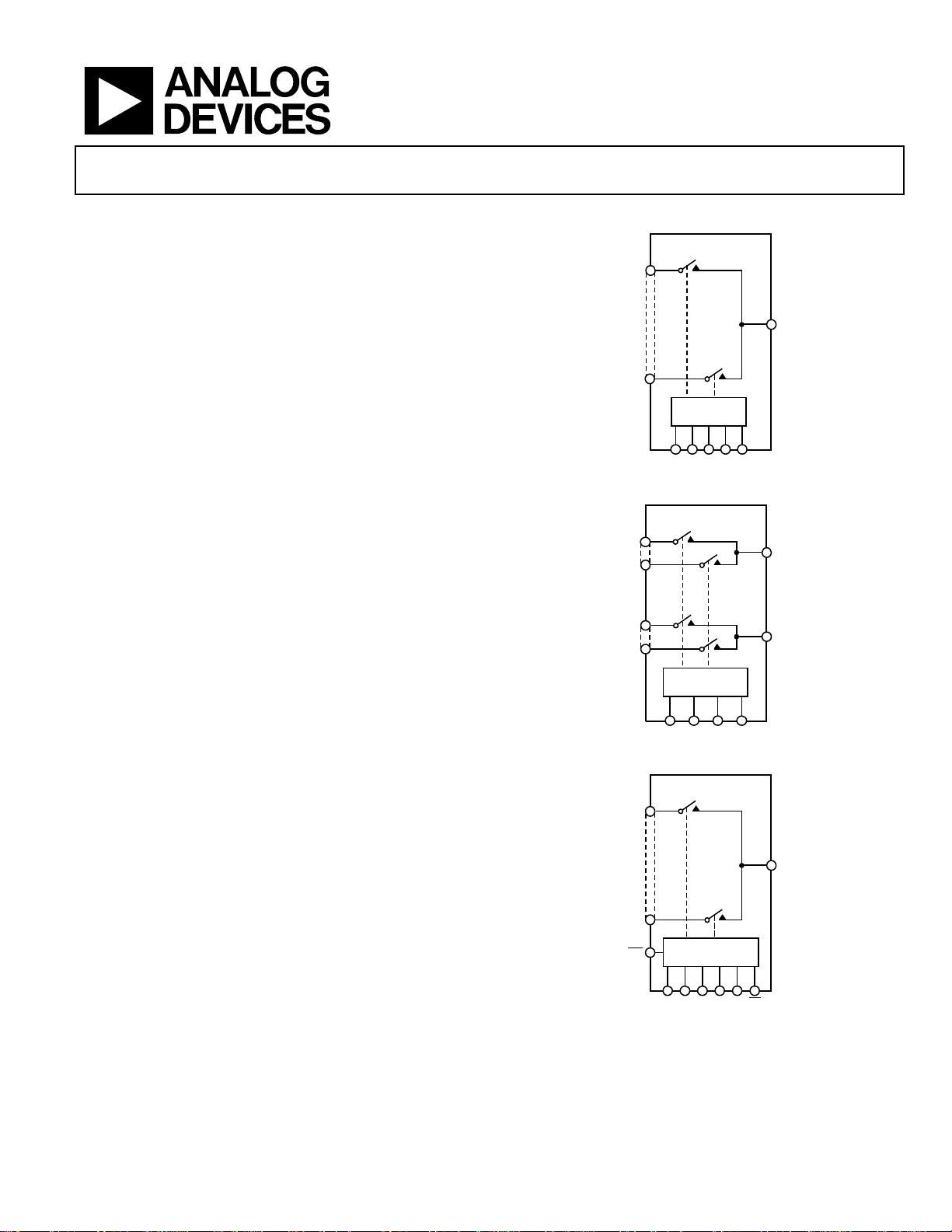
ADG406/ADG407/ADG426
FUNCTIONAL BLOCK DIAGRAMS
ADG406
S1
D
S16
1 OF 16
DECODER
A3
A1 A2 EN
S1A
S8A
S1B
S8B
A0
Figure 1.
ADG407
1 OF 8
DECODER
ENA0 A1 A2
Figure 2.
ADG426
S1
DA
DB
00026-001
00026-002
Rev. B
Information furnished by Analog Devices is believed to be accurate and reliable. However, no
responsibility is assumed by Analog Devices for its use, nor for any infringements of patents or other
rights of third parties that may result from its use. Specifications subject to change without notice. No
license is granted by implication or otherwise under any patent or patent rights of Analog Devices.
Trademarks and registered trademarks are the property of their respective owners.
D
S16
WR
One Technology Way, P.O. Box 9106, Norwood, MA 02062-9106, U.S.A.
Tel: 781.329.4700 www.analog.com
Fax: 781.461.3113 ©1994–2010 Analog Devices, Inc. All rights reserved.
DECODER/
LATCHES
A0
A1 A2 EN
Figure 3.
RS
00026-003
A3
Page 2

ADG406/ADG407/ADG426
TABLE OF CONTENTS
Features .............................................................................................. 1
Applications ....................................................................................... 1
Product Highlights ........................................................................... 1
Functional Block Diagrams ............................................................. 1
Revision History ............................................................................... 2
General Description ......................................................................... 3
Specifications ..................................................................................... 4
Dual Supply ................................................................................... 4
Single Supply ................................................................................. 6
REVISION HISTORY
5/10—Rev. A to Rev. B
Changes to Ordering Guide .......................................................... 20
6/09—Rev. 0 to Rev. A
Updated Format .................................................................. Universal
Removed T Grade ............................................................... Universal
Added Table 4 .................................................................................... 9
Added Table 6 .................................................................................. 10
Added Table 8 .................................................................................. 11
Updated Outline Dimensions ....................................................... 18
Changes to Ordering Guide .......................................................... 19
4/94—Revision 0: Initial Version
ADG426 Timing Diagrams ..........................................................7
Absolute Maximum Ratings ............................................................8
ESD Caution...................................................................................8
Pin Configurations and Function Descriptions ............................9
Typical Performance Characteristics ........................................... 12
Test Circuits ..................................................................................... 15
Terminology .................................................................................... 18
Outline Dimensions ....................................................................... 19
Ordering Guide .......................................................................... 20
Rev. B | Page 2 of 20
Page 3

ADG406/ADG407/ADG426
GENERAL DESCRIPTION
The ADG406, ADG407, and ADG426 are monolithic CMOS
analog multiplexers. The ADG406 and ADG426 switch one of
sixteen inputs to a common output as determined by the 4-bit
binary address lines: A0, A1, A2, and A3. The ADG426 has
on-chip address and control latches that facilitate microprocessor
interfacing. The ADG407 switches one of eight differential
inputs to a common differential output as determined by the
3-bit binary address lines A0, A1 and A2. An EN input on all
devices is used to enable or disable the device. When disabled,
all channels are switched off.
The ADG406/ADG407/ADG426 are designed on an enhanced
2
LC
MOS process that provides low power dissipation yet gives
high switching speed and low on resistance. These features make
the parts suitable for high speed data acquisition systems and
audio signal switching. Low power dissipation makes the parts
suitable for battery powered systems. Each channel conducts
equally well in both directions when on and has an input signal
range which extends to the supplies. In the off condition, signal
levels up to the supplies are blocked. All channels exhibit breakbefore-make switching action preventing momentary shorting
when switching channels. Inherent in the design is low charge
injection for minimum transients when switching the digital
inputs.
Rev. B | Page 3 of 20
Page 4

ADG406/ADG407/ADG426
SPECIFICATIONS
DUAL SUPPLY
VDD = +15 V ± 10%, VSS = −15 V ± 10%, GND = 0 V, unless otherwise noted.
Table 1.
Parameter1 +25°C −40°C to +85°C Unit Test Conditions/Comments
ANALOG SWITCH
Analog Signal Range VSS to VDD V
RON 50 Ω typ VD = ±10 V, IS = −1 mA
80 125 Ω max VDD = +13.5 V, VSS = −13.5 V
RON Match 4 Ω typ VD = 0 V, IS = −1 mA
LEAKAGE CURRENTS VDD = +16.5 V, VSS = −16.5 V
Source Off Leakage IS (Off) ±0.5 ±20 nA max
Drain Off Leakage ID (Off)
ADG406, ADG426 ±1 ±20 nA max
ADG407 ±1 ±20 nA max
Channel On Leakage ID, IS (On) VS = VD = ±10 V; see Figure 28
ADG406, ADG426 ±1 ±20 nA max
ADG407 ±1 ±20 nA max
DIGITAL INPUTS
Input High Voltage, V
Input Low Voltage, V
2.4 V min
INH
0.8 V max
INL
Input Current
I
or I
±1 A max VIN = 0 or V
INL
INH
CIN, Digital Input Capacitance 8 pF typ f = 1 MHz
DYNAMIC CHARACTERISTICS2
t
120 ns typ
TRANSITION
150 250 ns max
Break Before Make Delay, t
10 10 ns min RL = 300 Ω, CL = 35 pF; VS = +5 V, see Figure 30
OPEN
tON (EN, WR)
120 175 ns typ R
160 225 ns max
t
(EN, RS)
OFF
110 130 ns typ R
150 180 ns max
ADG426 Only
tW, Write Pulse Width 100 ns min
tS, Address, Enable Setup Time 100 ns min
tH, Address, Enable Hold Time 10 ns min
tRS, Reset Pulse Width 100 ns min VS = +5 V
Charge Injection 8 pC typ VS = 0 V, RS = 0 Ω, CL = 1 nF;
See Figure 34
Off Isolation −75 dB typ RL = 1 k Ω, f = 100 kHz;
V
Channel-to-Channel Crosstalk 85 dB typ RL = 1 k Ω, f = 100 kHz, see Figure 36
CS (Off) 5 pF typ f = 1 MHz
CD (Off) f = 1 MHz
ADG406, ADG426 50 pF typ
ADG407 25 pF typ
CD, CS (On) f = 1 MHz
ADG406, ADG426 60 pF typ
ADG407 40 pF typ
= ±10 V, VS = +10 V, see Figure 26
V
D
= ±10 V, VS = +10 V; see Figure 27
V
D
DD
= 300 Ω, CL = 35 pF; V1 = ±10 V, V2 = +10 V; see Figure 29
R
L
= 300 Ω, CL = 35 pF; VS = 5 V, see Figure 31
L
= 300 Ω, CL = 35 pF; VS = 5 V, see Figure 31
L
= 0 V, see Figure 35
EN
Rev. B | Page 4 of 20
Page 5
ADG406/ADG407/ADG426
Parameter1 +25°C −40°C to +85°C Unit Test Conditions/Comments
POWER REQUIREMENTS VDD = +16.5 V, VSS = −16.5 V
I
1 A typ VIN = 0 V, VEN = 0 V
DD
5 A max
I
1 A typ
SS
5 A max
I
100 A typ VIN = 0 V, VEN = 2.4 V
DD
200 500 A max
I
1 A typ
SS
5 A max
1
Temperature ranges is −40°C to +85°C.
2
Guaranteed by design, not subject to production test.
Rev. B | Page 5 of 20
Page 6

ADG406/ADG407/ADG426
SINGLE SUPPLY
VDD = +12 V ± 10%, VSS = 0 V, GND = 0 V, unless otherwise noted.
Table 2.
Parameter1 +25°C −40°C to +85°C Unit Test Conditions/Comments
ANALOG SWITCH
Analog Signal Range 0 to VDD V
RON 90 Ω typ VD = +3 V, +8.5 V, IS = −1 mA;
125 200 Ω max VDD = +10.8 V
LEAKAGE CURRENTS VDD = +13.2 V
Source Off Leakage IS (Off) ±0.5 ±20 nA max VD = 8 V/0.1 V, VS = 0.1 V/8 V; see Figure 26
Drain Off Leakage ID (Off) VD = 8 V/0.1 V, VS = 0.1 V/8 V; see Figure 27
ADG406, ADG426 ±1 ±20 nA max
ADG407 ±1 ±20 nA max
Channel On Leakage ID, IS (On) VS = VD = 8 V/0.1 V, see Figure 28
ADG406, ADG426 ±1 ±20 nA max
ADG407 ±1 ±20 nA max
DIGITAL INPUTS
Input High Voltage, V
Input Low Voltage, V
Input Current
I
or I
±1 µA max VIN = 0 or VDD
INL
INH
CIN, Digital Input Capacitance 8 pF typ f = 1 MHz
DYNAMIC CHARACTERISTICS2
t
180 ns typ RL = 300 Ω, CL = 35 pF; V1 = 8 V/0 V, V2 = 0 V/8 V; see Figure 29
TRANSITION
220 350 ns max
Break Before Make Delay, t
tON (EN, WR)
240 350 ns max VS = +5 V, see Figure 31
t
(EN, RS)
OFF
180 220 ns max
ADG426 Only
tW, Write Pulse Width 100 ns min
tS, Address, Enable Setup Time 100 ns min
tH, Address, Enable Hold Time 10 ns min
tRS, Reset Pulse Width 100 ns min VS = +5 V
Charge Injection 5 pC typ VS = 6 V, RS = 0 Ω, CL = 1 nF; see Figure 34
Off Isolation −75 dB typ RL = 1 kΩ, f = 100 kHz; see Figure 35
Channel-to-Channel Crosstalk 85 dB typ RL = 1 kΩ, f = 100 kHz; see Figure 36
CS (Off) 8 pF typ f = 1 MHz
CD (Off) f = 1 MHz
ADG406, ADG426 80 pF typ
ADG407 40 pF typ f = 1 MHz
CD, CS (On)
ADG406, ADG426 100 pF typ
ADG407 50 pF typ
POWER REQUIREMENTS VDD = +13.2 V
IDD 1 µA typ VIN = 0 V, VEN = 0 V
5 µA max
IDD 100 µA typ VIN = 0 V, VEN = 2.4 V
200 500 µA max
1
Temperature range is −40°C to +85°C.
2
Guaranteed by design, not subject to production test.
2.4 V min
INH
0.8 V max
INL
10 ns typ RL = 300 Ω, CL = 35 pF; VS = 5 V, see Figure 30
OPEN
180 ns typ R
135 ns typ R
Rev. B | Page 6 of 20
= 300 Ω, CL = 35 pF;
L
= 300 Ω, CL = 35 pF; VS = 5 V, see Figure 31
L
Page 7

ADG406/ADG407/ADG426
V
A
V
ADG426 TIMING DIAGRAMS
3
WR
0V
3V
0, A1, A2, (A3)
EN
0V
Figu re 4. T iming Sequence for Latching the Switch Address and Enable Inputs
Figure 4 shows the timing sequence for latching the switch
address and enable inputs. The latches are level sensitive;
therefore, while
WR
the switches respond to the address and enable inputs. This
input data is latched on the rising edge of
50%
2V
50%
t
W
t
S
0.8V
t
H
is held low, the latches are transparent and
WR
.
00026-009
Figure 5 shows the reset pulse width, trs, and the reset turn off
time, t
Note that all digital input signals rise and fall times are
measured from 10% to 90% of 3 V; t
3
RS
SWITCH
OUTPUT
0V
V
0
0V
50% 5 0%
t
W
t
(RS)
OFF
Figure 5. Reset Pulse Width and Reset Turn Off Time
(RS).
OFF
= tF = 20 ns.
R
0.8V
0
00026-010
Rev. B | Page 7 of 20
Page 8

ADG406/ADG407/ADG426
ABSOLUTE MAXIMUM RATINGS
TA = 25°C unless otherwise noted.
Table 3.
Parameter Rating
VDD to VSS 44 V
VDD to GND −0.3 V to +25 V
VSS to GND +0.3 V to −25 V
Analog, Digital Inputs1
Continuous Current, S or D 20 mA
Peak Current, S or D 40 mA
Operating Temperature Range
Industrial (B Version) −40°C to +85°C
Storage Temperature Range −65°C to +150°C
Junction Temperature 150°C
Plastic Package
θJA, Thermal Impedance 75°C/W
Lead Temperature, Soldering
(10 sec)
PLCC Package
θJA, Thermal Impedance 80°C/W
Lead Temperature, Soldering
Vapor Phase (60 sec) 215°C
Infrared (15 sec) 220°C
SSOP Package
θJA, Thermal Impedance 122°C/W
Lead Temperature, Soldering
Vapor Phase (60 sec) 215°C
Infrared (15 sec) 220°C
1
Overvoltages at A, S, D, WR, or RS will be clamped by internal diodes. Current
should be limited to the maximum ratings given.
− 2 V to VDD + 2 V or 20 mA,
V
SS
whichever occurs first
(Pulsed at 1 ms, 10% duty
cycle max)
260°C
Stresses above those listed under Absolute Maximum Ratings
may cause permanent damage to the device. This is a stress
rating only; functional operation of the device at these or any
other conditions above those indicated in the operational
section of this specification is not implied. Exposure to absolute
maximum rating conditions for extended periods may affect
device reliability.
ESD CAUTION
Rev. B | Page 8 of 20
Page 9

ADG406/ADG407/ADG426
PIN CONFIGURATIONS AND FUNCTION DESCRIPTIONS
V
1
DD
NC
2
NC
3
4
S16
S15
5
S14
6
S13
7
(Not to Scale)
S12
8
9
S11
10
S10
11
S9
12
GND
13
NC
14
A3
NC = NO CONNECT
ADG406
TOP VIEW
D
28
27
V
SS
S8
26
S7
25
24
S6
S5
23
S4
22
21
S3
S2
20
S1
19
EN
18
17
A0
16
A1
15
A2
00026-004
Figure 6. 28-Lead PDIP
Table 4. Pin Function Descriptions
Pin No. Mnemonic Description
1 VDD Most Positive Power Supply Potential.
2, 3, 13 NC No Connect.
4 to 11 S16 to S9
12 GND
14 to 17 A3 to A0
18 EN
Source Terminal 16 to Source Terminal 9. These pins can be inputs or outputs.
Ground (0 V) Reference.
Logic Control Input.
Active High Digital Input. When this pin is low, the device is disabled and all switches are turned off. When this pin
is high, the Ax logic inputs determine which switch is turned on.
19 to 26 S1 to 8
27 V
Most Negative Power Supply Potential. In single-supply applications, this pin can be connected to ground.
SS
Source Terminal 1 to Source Terminal 8. These pins can be inputs or outputs.
28 D Drain Terminal. This pin can be an input or an output.
S16NCNC
5
S15
S14
S13
S12
S11
S10
INDENTFIE R
6
7
8
9
10
S9
11
12 13 14 15 16 17 18
GND
NC = NO CONNECT
Figure 7. 28-Lead PLCC
VDDD
1282726234
PIN 1
ADG406
TOP VIEW
(Not to scale)
A3A2A1
NC
VSSS8
A0
EN
25
S7
24
S6
23
S5
22
S4
21
S3
20
S2
S1
19
00026-005
Table 5. Truth Table (ADG406)
A3 A2 A1 A0 EN On Switch
X X X X 0 None
0 0 0 0 1 1
0 0 0 1 1
0 0 1 0 1
0 0 1 1 1
0 1 0 0 1
0 1 0 1 1
0 1 1 0 1
0 1 1 1 1
1 0 0 0 1
1 0 0 1 1
1 0 1 0 1
1 0 1 1 1
1 1 0 0 1
1 1 0 1 1
1 1 1 0 1
2
3
4
5
6
7
8
9
10
11
12
13
14
15
1 1 1 1 1 16
Rev. B | Page 9 of 20
Page 10

ADG406/ADG407/ADG426
V
1
DD
2
DB
3
NC
4
S8B
5
S7B
ADG407
6
S6B
TOP VIEW
7
S5B
(Not to Scale)
8
S4B
9
S3B
10
S2B
11
S1B
12
GND
13
NC
14
NC
NC = NO CONNECT
Figure 8. 28-Lead PDIP
Table 6. Pin Function Descriptions
Pin No. Mnemonic Description
1 VDD Most Positive Power Supply Potential.
2 DB Drain Terminal B. This pin can be an input or an output.
3, 13, 14 NC
4 to 11 S8B to S1B
12 GND
15 to 17 A2 to A0
18 EN
No Connect.
Source Terminal 8B to Source Terminal 1B. These pins can be inputs or outputs.
Ground (0 V) Reference.
Logic Control Input.
Active High Digital Input. When this pin is low, the device is disabled and all switches are turned off. When this pin
is high, the Ax logic inputs determine which switch is turned on.
19 to 26 S1A to S8A
27 V
Most Negative Power Supply Potential. In single-supply applications, this pin can be connected to ground.
SS
Source Terminal 1A to Source Terminal 8A. These pins can be inputs or outputs.
28 DA Drain Terminal A. This pin can be an input or an output.
DA
28
27
V
SS
S8A
26
S7A
25
24
S6A
S5A
23
S4A
22
21
S3A
S2A
20
S1A
19
EN
18
17
A0
16
A1
15
A2
00026-006
S7B
S6B
S5B
S4B
S3B
S2B
S1B
S8BNCDB
5
6
7
8
9
10
11
PIN 1
INDENTFIER
ADG407
TOP VIEW
(Not to scale)
12 13 14 15 16 17 18
NC
NC
GND
NC = NO CONNECT
VDDDA
1282726234
A2A1A0
VSSS8A
EN
25
S7A
24
S6A
23
S5A
22
S4A
21
S3A
20
S2A
S1A
19
00026-007
Figure 9. 28-Lead PLCC
Table 7. Truth Table (ADG407)
A2 A1 A0 EN On Switch Pair
X X X 0 None
0 0 0 1 1
0 0 1 1
0 1 0 1
0 1 1 1
1 0 0 1
1 0 1 1
1 1 0 1
2
3
4
5
6
7
1 1 1 1 8
Rev. B | Page 10 of 20
Page 11

ADG406/ADG407/ADG426
V
1
DD
2
NC
3
RS
S16
4
5
S15
S14
S13
S12
S11
S10
S9
GND
WR
A3
ADG426
6
TOP VIEW
7
(Not to Scale)
8
9
10
11
12
13
14
NC = NO CO NNECT
Figure 10. 28-Lead PDIP/SSOP
Table 8. Pin Function Descriptions
Pin No. Mnemonic Description
1 VDD Most Positive Power Supply Potential.
2 NC No Connect.
3
RS Active Low Logic Input. When this pin is low, all switches are open, and address and enable latches registers are
cleared to 0.
4 to 11 S16 to S9
12 GND
13
WR
Source Terminal 16 to Source Terminal 9. These pins can be inputs or outputs.
Ground (0 V) Reference.
The rising edge of the WR signal latches the state of the address control lines and the enable line.
14 to 17 A3 to A0 Logic Control Input.
18 EN
Active High Digital Input. When this pin is low, the device is disabled and all switches are turned off. When this pin
is high, the Ax logic inputs determine which switch is turned on.
19 to 26 S1 to S8
27 V
Most Negative Power Supply Potential. In single-supply applications, this pin can be connected to ground.
SS
Source Terminal 1 to Source Terminal 8. These pins can be inputs or outputs.
28 D Drain Terminal. This pin can be an input or an output.
D
28
V
27
SS
26
S8
S7
25
S6
24
23
S5
S4
22
S3
21
20
S2
S1
19
EN
18
17
A0
A1
16
A2
15
00026-008
Table 9. Truth Table (ADG426)
A3 A2 A1 A0 EN
X X X X X
WR
RS
On switch
1 Retains previous switch condition
X X X X X X 0 None (address and enable latches cleared)
X X X X 0 0 1
0 0 0 0 1 0 1
0 0 0 1 1 0 1
0 0 1 0 1 0 1
0 0 1 1 1 0 1
0 1 0 0 1 0 1
0 1 0 1 1 0 1
0 1 1 0 1 0 1
0 1 1 1 1 0 1
1 0 0 0 1 0 1
1 0 0 1 1 0 1
1 0 1 0 1 0 1
1 0 1 1 1 0 1
1 1 0 0 1 0 1
1 1 0 1 1 0 1
1 1 1 0 1 0 1
None
1
2
3
4
5
6
7
8
9
10
11
12
13
14
15
1 1 1 1 1 0 1 16
Rev. B | Page 11 of 20
Page 12

ADG406/ADG407/ADG426
TYPICAL PERFORMANCE CHARACTERISTICS
150
TA = 25°C
120
90
VDD = +10V
= –10V
V
(Ω)
ON
R
SS
60
30
VDD = +15V
= –15V
V
SS
0
–15 15–10–50 510
VD (VS) (V)
VDD = +5V
=–5V
V
SS
VDD = +12V
V
SS
= –12V
Figure 11. RON as a Function of VD (VS): Dual Supplies
100
80
VDD = +15V
V
SS
00026-011
= –15V
400
350
300
250
(Ω)
200
ON
R
150
100
50
0
012.5 5.0 7.5 10 12.5
VDD = +5V
V
SS
VDD = +15V
= 0V
V
SS
=0V
VDD = +10V
V
=0V
SS
VD (VS) (V)
Figure 14. RON as a Function of VD (VS): Single Supplies
150
120
TA = 25°C
VDD = +12V
=0V
V
SS
VDD = 12V
=0V
V
SS
00026-014
5
60
(Ω)
ON
R
40
20
0
–15 15–10–50 510
85°C
25°C
VD (VS) (V)
125°C
Figure 12. RON as a Function of VD (VS) for Different Temperatures
0.10
VDD = +15V
= –15V
V
0.08
0.06
0.04
0.02
LEAKAGE CURRENT ( nA)
–0.02
SS
=+25°C
T
A
0
–15 15–10–50 510
VD (VS) (V)
IS(OFF)
ID(ON)
ID(OFF)
Figure 13. Leakage Currents as a Function of VD (VS)
90
(Ω)
ON
R
60
30
00026-012
0
01246810
85°C
25°C
VD (VS) (V)
125°C
00026-015
2
Figure 15. RON as a Function of VD (VS) for Different Temperatures
0.02
VDD = +12V
=0V
V
SS
=+25°C
T
A
0.01
IS(OFF)
0
ID(OFF)
LEAKAGE CURRENT ( nA)
–0.01
00026-013
–0.02
01246810
ID(ON)
VD (VS) (V)
00026-016
2
Figure 16. Leakage Currents as a Function of VD (VS)
Rev. B | Page 12 of 20
Page 13

ADG406/ADG407/ADG426
100
VDD = +15V
V
= –15V
SS
100
VDD = +15V
= –15V
V
10
SS
10
(mA)
DD
I
1
0.1
100 1k 10k 100k 1M 10M
FREQUENCY (Hz )
EN = 2.4V
EN = 0V
Figure 17. Positive Supply Current vs. Switching Frequency
160
t
ON
140
120
(ns)
t
100
80
60
1357911131
VIN (V)
VDD = +15V
V
SS
t
TRANSITI ON
= –15V
t
OFF
Figure 18. Switching Time vs. VIN (Bipolar Supply)
300
VIN = +5V
200
t
(ns)
t
t
100
t
OFF
TRANSITION
ON
00026-017
00026-018
5
1
EN = 2.4V
0.1
(mA)
SS
I
0.01
0.001
0.0001
100 1k 10k 100k 1M 10M
FREQUENCY (Hz )
EN = 0V
Figure 20. Negative Supply Current vs. Switching Frequency
220
200
t
ON
180
160
(ns)
t
140
120
100
80
246810
VIN (V)
VDD = +12V
=0V
V
SS
t
TRANSITION
t
OFF
Figure 21. Switching Time vs. VIN (Single Supply)
500
VIN = +5V
400
300
(ns)
t
200
100
t
TRANSITION
t
ON
t
OFF
00026-020
00026-021
12
0
±5 ±7 ±9 ±11 ±13 ±15 ±17 ±19 ±21
SUPPLY VOLTAGE (V)
Figure 19. Switching Time vs. Bipolar Supply
00026-019
Rev. B | Page 13 of 20
0
5 7 9 11 13 15
SUPPLY VOLTAGE (V)
Figure 22. Switching Time vs. Single Supply
00026-022
Page 14

ADG406/ADG407/ADG426
140
120
VDD = +15V
V
= –15V
SS
140
120
VDD = +15V
V
= –15V
SS
100
80
OFF ISOLATION (dB)
60
40
100 1k 10k 100k 1M 10M
FREQUENCY (Hz )
Figure 23. Off Isolation vs. Frequency
00026-023
100
80
CROSSTALK (d B)
60
40
100 1k 10k 100k 1M 10M
FREQUENCY (Hz )
Figure 24. Crosstalk vs. Frequency
00026-024
Rev. B | Page 14 of 20
Page 15

ADG406/ADG407/ADG426
V
VDDV
VDDV
VSSV
VSSV
TEST CIRCUITS
I
DS
SS
V1
S D
S
RON = V1/I
DS
00026-025
V
S
Figure 25. On Resistance
V
V
SS
DD
S16
V
DDVSS
S1
EN
D
+0.8V
00026-026
V
S
S2
(OFF)
I
S
A
V
S
V
D
Figure 26. IS (Off)
S1
S2
S16
S1
S16
V
DDVSS
EN
Figure 27. ID (Off)
SS
V
DDVSS
EN
Figure 28. ID (On)
(OFF)
I
D
D
A
V
D
+0.8V
00026-027
(ON)
I
D
D
A
V
D
+2.4V
00026-028
DD
3V
V
A3
V
50Ω
IN
A2
A1
A0
2.4V
EN
RS
GND
DD
S2 THRU S15
ADG426
WR
V
SS
S1
V
1
S16
1
V
2
D
R
L
300Ω
C
L
35pF
V
OUT
ADDRESS
DRIVE (V
)
IN
50%
50%
90%
V
OUT
90%
1
SIMILAR CO NNECTION FOR ADG406/ADG407
t
TRANSITION
Figure 29. Switching Time of Multiplexer, t
TRANSITION
t
TRANSITI ON
00026-029
DD
V
A3
V
50Ω
IN
A2
A1
A0
DD
S2 THRU S15
ADG426
V
SS
S16
1
RS
2.4V
1
SIMILAR CO NNECTION FOR ADG406/ADG407
EN
GND
WR
S1
D
R
L
300Ω
V
S
C
35pF
V
L
Figure 30. Break-Before-Make Delay, t
ADDRESS
DRIVE (V
OUT
3V
)
IN
OUTPUT
0V
OPEN
80%
t
OPEN
80%
00026-030
Rev. B | Page 15 of 20
Page 16

ADG406/ADG407/ADG426
VSSV
VSSV
VSSV
DD
V
A3
A2
A1
A0
2.4V
V
IN
1
SIMILAR CO NNECTION FOR ADG406/ADG 407
50Ω
RS
EN
GND
DD
S2 THRU S16
ADG426
WR
V
SS
1
S1
D
R
L
300Ω
V
S
Figure 31. Enable Delay, t
C
L
35pF
V
OUT
ENABLE
DRIVE (V
OUTPUT
(EN), t
ON
3V
50%
90%
t
(EN)
OFF
00026-031
(EN)
50%
90%
t
(EN)
ON
)
IN
0V
V
O
0V
OFF
DD
2.4V
V
A3
A2
A1
A0
EN
RS
V
WR
RS
V
WR
DD
S2 THRU S16
ADG426
GND
V
SS
S1
D
R
L
300Ω
V
S
V
OUT
C
L
35pF
Figure 32. Write Turn-On Time, t
WR
OUTPUT
3V
50%
0V
V
0
0V
(WR)
ON
t
(WR)
ON
0.2V
0
00026-032
DD
DD
S2 THRU S16
ADG426
GND
WR
V
SS
S1
D
R
L
300Ω
V
S
V
OUT
C
L
35pF
Figure 33. Reset Turn-Off Time, t
RS
OUTPUT
3V
50%
0V
t
(RS)
OFF
V
0
0V
(RS)
OFF
0.8V
0
00026-033
2.4V
V
V
A3
A2
A1
A0
EN
RS
IN
Rev. B | Page 16 of 20
Page 17

ADG406/ADG407/ADG426
VSSV
V
V
DD
V
A3
A2
A1
R
S
V
S
V
IN
1
SIMILAR CO NNECTION F OR ADG406/ADG 407.
A0
S
EN
DD
ADG426
GND
WR
V
SS
RS
1
D
2.4V
C
1nF
V
L
OUT
LOGIC
INPUT
(V
V
OUT
3V
)
IN
ΔV
Q
INJ
= CL× ΔV
OUT
OUT
00026-034
Figure 34. Charge Injection
DD
V
S16
S2
S1
A0
ADG426
A1
A2
A3
EN
RS
GND
DD
WR
D
V
OUT
1kΩ
1
V
SS
2.4V
A3
A2
A1
A0
RS
EN
GND
DD
V
DD
ADG426
WR
V
1
S16
SS
V
IN
1kΩ
S1
V
IN
D
R
1kΩ
V
OUT
L
2.4V
V
1
SIMILAR CONNECTION FOR ADG406/ADG 407.
SS
Figure 35. Off Isolation
1
00026-035
SIMILAR CO NNECTION F OR ADG406/ADG 407.
Figure 36. Crosstalk
V
SS
00026-036
Rev. B | Page 17 of 20
Page 18

ADG406/ADG407/ADG426
TERMINOLOGY
t
(EN)
VDD
Most positive power supply potential.
V
SS
Most negative power supply potential in dual supplies. In single
supply applications, it may be connected to ground.
GND
Ground (0 V) reference.
R
ON
Ohmic resistance between the D and S terminals.
R
Match
ON
Difference between the R
(Off)
I
S
of any two channels.
ON
Source leakage current when the switch is off.
I
(Off)
D
Drain leakage current when the switch is off.
I
, IS (On)
D
Channel leakage current when the switch is on.
V
(VS)
D
Analog voltage on Terminal D, Terminal S.
C
(Off)
S
Channel input capacitance for off condition.
C
(Off)
D
Channel output capacitance for off condition.
C
, CS (ON)
D
On switch capacitance.
C
IN
Digital input capacitance.
t
(EN)
ON
Delay time between the 50% and 90% points of the digital input
and switch on condition.
OFF
Delay time between the 50% and 90% points of the digital input
and switch off condition.
t
TRANSITION
Delay time between the 50% and 90% points of the digital
inputs and the switch on condition when switching from
one address state to another.
t
OPEN
Off time measured between 80% points of both switches when
switching from one address state to another.
V
INL
Maximum input voltage for Logic 0.
V
INH
Minimum input voltage for Logic 1.
I
(I
)
INL
INH
Input current of the digital input.
Crosstalk
A measure of unwanted signal which is coupled through from
one channel to another as a result of parasitic capacitance.
Off Isolation
A measure of unwanted signal coupling through an off channel.
Charge Injection
A measure of the glitch impulse transferred from the digital
input to the analog output during switching.
I
DD
Positive supply current.
I
SS
Negative supply current.
Rev. B | Page 18 of 20
Page 19

ADG406/ADG407/ADG426
OUTLINE DIMENSIONS
1.565 (39.75)
1.380 (35.05)
0.250 (6.35)
0.200 (5.08)
0.115 (2.92)
0.022 (0.56)
0.014 (0.36)
MAX
28
114
0.100 (2.54)
BSC
0.070 (1.78)
0.050 (1.27)
15
0.580 (14.73)
0.485 (12.31)
0.015
(0.38)
MIN
SEATING
PLANE
0.005 (0.13)
MIN
0.015 (0.38)
GAUGE
PLANE
0.625 (15.88)
0.600 (15.24)
0.700 (17.78)
MAX
0.195 (4.95)
0.125 (3.17)
0.015 (0.38)
0.008 (0.20)
CONTROLL ING DIMENSIONS ARE IN INCHES; MIL LIMETER DIMENSIONS
(IN PARENTHESES) ARE ROUNDED-O FF INCH EQ UIVALENTS FOR
REFERENCE ON LY AND ARE NOT APPROPRI ATE FOR USE IN DESIGN.
CORNER LEADS M AY BE CONFIGURED AS WHOLE LEADS.
COMPLIANT TO JEDEC STANDARDS MS-011
071006-A
Figure 37. 28-Lead Plastic Dual In-Line Package {PDIP}
Wide Body
(N-28-2)
Dimensions shown in inches and (millimeters)
0.180 (4.57)
0.120 (3.04)
0.090 (2.29)
0.165 (4.19)
0.020 (0.51)
MIN
0.021 (0.53)
0.013 (0.33)
0.032 (0.81)
0.026 (0.66)
0.045 (1.14)
0.025 (0.64)
0.430 (10.92)
0.390 (9.91)
R
BOTTOM
VIEW
(PINS UP)
042508-A
0.048 (1.22)
0.042 (1.07)
0.048 (1.22)
0.042 (1.07)
4
5
11
12
0.456 (11.582)
0.450 (11.430)
0.495 (12.57)
0.485 (12.32)
0.056 (1.42)
0.042 (1.07)
26
25
PIN 1
IDENTIFIER
TOP VIEW
(PINS DOWN)
CONTROLL ING DIMENS IONS ARE IN I NCHES; MILL IMETER DI MENSIONS
(IN PARENTHESES ) ARE ROUNDED-OF F INCH EQUI VALENTS FOR
REFERENCE ONLY AND ARE NOT APPROPRIATE FO R USE IN DESIGN.
0.050
(1.27)
BSC
19
18
SQ
SQ
COMPLIANT TO JEDEC STANDARDS MO-047-AB
Figure 38. 28-Lead Plastic Leaded Chip Carrier [PLCC]
(P-28)
Dimensions shown in inches and (millimeters)
Rev. B | Page 19 of 20
Page 20

ADG406/ADG407/ADG426
28
1
2.00 MAX
0.05 MIN
COPLANARITY
0.10
0.65 BSC
10.50
10.20
9.90
15
5.60
5.30
8.20
5.00
7.80
1.85
1.75
1.65
SEATING
PLANE
7.40
8°
4°
0°
14
0.38
0.22
COMPLIANT TO JEDEC STANDARDS MO-150-AH
0.25
0.09
0.95
0.75
0.55
060106-A
Figure 39. 28-Lead Shrink Small Outline Package [SSOP]
(RS-28)
Dimensions shown in millimeters
ORDERING GUIDE
Model1 Temperature Range Package Description Package Option2
ADG406BN −40°C to +85°C 28-Lead PDIP N-28-2
ADG406BNZ −40°C to +85°C 28-Lead PDIP N-28-2
ADG406BP −40°C to +85°C 28-Lead PLCC P-28
ADG406BP-REEL −40°C to +85°C 28-Lead PLCC P-28
ADG406BPZ −40°C to +85°C 28-Lead PLCC P-28
ADG406BPZ-REEL −40°C to +85°C 28-Lead PLCC P-28
ADG407BN −40°C to +85°C 28-Lead PDIP N-28-2
ADG407BNZ −40°C to +85°C 28-Lead PDIP N-28-2
ADG407BP −40°C to +85°C 28-Lead PLCC P-28
ADG407BP-REEL −40°C to +85°C 28-Lead PLCC P-28
ADG407BPZ −40°C to +85°C 28-Lead PLCC P-28
ADG407BPZ-RL −40°C to +85°C 28-Lead PLCC P-28
ADG407BCHIPS −40°C to +85°C DIE
ADG426BN −40°C to +85°C 28-Lead PDIP N-28-2
ADG426BNZ −40°C to +85°C 28-Lead PDIP N-28-2
ADG426BRS −40°C to +85°C 28-Lead SSOP RS-28
ADG426BRS-REEL −40°C to +85°C 28-Lead SSOP RS-28
ADG426BRS-REEL7 −40°C to +85°C 28-Lead SSOP RS-28
ADG426BRSZ −40°C to +85°C 28-Lead SSOP RS-28
ADG426BRSZ-REEL −40°C to +85°C 28-Lead SSOP RS-28
1
Z = RoHS Compliant Part.
2
N = Plastic DIP, P = Plastic Leaded Chip Carrier (PLCC), RS = Shrink Small Outline Package (SSOP).
©1994–2010 Analog Devices, Inc. All rights reserved. Trademarks and
registered trademarks are the property of their respective owners.
D00026-0-5/10(B)
Rev. B | Page 20 of 20
 Loading...