

Page 1
Low Voltage, 1.15 V to 5.5 V, 8-Channel
V
V
FEATURES
Bidirectional logic level translation
Operates from 1.15 V to 5.5 V
Low quiescent current < 1 μA
No direction pin
APPLICATIONS
Low voltage ASIC level translation
Smart card readers
Cell phones and cell phone cradles
Portable communication devices
Telecommunications equipment
Network switches and routers
Storage systems (SAN/NAS)
Computing/server applications
GPS
Portable POS systems
Low cost serial interfaces
Bidirectional Logic Level Translators
ADG3308/ADG3308-1
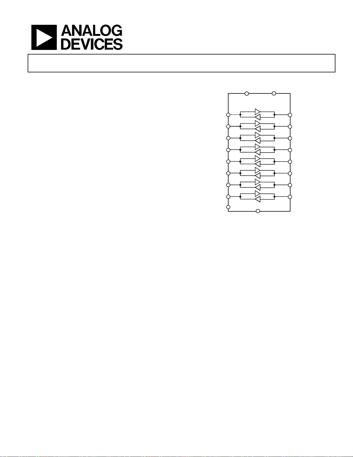
FUNCTIONAL BLOCK DIAGRAM
CCA
ADG3308/ADG3308-1/
ADG3308-2
A1
A2
A3
A4 Y4
A5
A6
A7
A8
EN
GND
Figure 1.
CCY
Y1
Y2
Y3
Y5
Y6
Y7
Y8
4865-001
GENERAL DESCRIPTION
The ADG3308/ADG3308-1/ADG3308-2 are bidirectional level
translators containing eight bidirectional channels. They can be
used in multivoltage digital system applications, such as a data
transfer between a low voltage DSP controller and a higher
voltage device. The internal architecture allows the device to
perform bidirectional level translation without an additional
signal to set the direction in which the translation takes place.
The voltage applied to V
of the device, and V
operation, V
must always be less than V
CCA
compatible logic signals applied to the A side of the device
appear as V
compatible levels on the Y side. Similarly, V
CCY
compatible logic levels applied to the Y side of the device appear
as V
compatible logic levels on the A side.
CCA
The enable pin (EN) provides three-state operation on both the
A side and the Y side pins. When the EN pin is pulled low, the
terminals on both sides of the device are in the high impedance
state. For normal operation, EN should be driven high.
sets the logic levels on the A side
CCA
sets the levels on the Y side. For proper
CCY
. The V
CCY
CCA
CCY
The ADG3308 is available in a compact 20-lead TSSOP and
a 20-lead LFCSP, the ADG3308-1 is available in a 20-ball
WLCSP, and the ADG3308-2 is available in a backside-coated
20-ball WLCSP. The EN pin is referred to the V
voltage for the ADG3308 and to the V
supply voltage for the
CCA
CCY
supply
ADG3308-1 and ADG3308-2.
The ADG3308/ADG3308-1/ADG3308-2 are guaranteed to
operate over the 1.15 V to 5.5 V supply voltage range and the
extended −40°C to +85°C temperature range.
PRODUCT HIGHLIGHTS
1. Bidirectional logic level translation.
2. Fully guaranteed over the 1.15 V to 5.5 V supply range.
3. No direction pin.
4. Packages: 20-lead TSSOP and 20-lead LFCSP (ADG3308),
20-ball WLCSP (ADG3308-1), and backside-coated 20-ball
WLCSP (ADG3308-2).
Rev. C
Information furnished by Analog Devices is believed to be accurate and reliable. However, no
responsibility is assumed by Anal og Devices for its use, nor for any infringements of patents or ot her
rights of third parties that may result from its use. Specifications subject to change without notice. No
license is granted by implication or otherwise under any patent or patent rights of Analog Devices.
Trademarks and registered trademarks are the property of their respective owners.
One Technology Way, P.O. Box 9106, Norwood, MA 02062-9106, U.S.A.
Tel: 781.329.4700 www.analog.com
Fax: 781.461.3113 ©2005–2007 Analog Devices, Inc. All rights reserved.
Page 2

ADG3308/ADG3308-1
TABLE OF CONTENTS
Features .............................................................................................. 1
Applications....................................................................................... 1
Functional Block Diagram .............................................................. 1
General Description ......................................................................... 1
Product Highlights........................................................................... 1
Revision History ............................................................................... 2
Specifications..................................................................................... 3
Absolute Maximum Ratings............................................................ 6
ESD Caution.................................................................................. 6
Pin Configurations and Function Descriptions ........................... 7
Typical Performance Characteristics............................................. 8
Test Cir c ui t s .....................................................................................12
Te r mi n ol o g y .................................................................................... 15
REVISION HISTORY
9/07—Rev. B to Rev. C
Updated Outline Dimensions....................................................... 19
7/07—Rev. A to Rev. B
Added Backside-Coated WLCSP Package ......................Universal
Changes to Input Driving Requirements Section ...................... 16
Updated Outline Dimensions....................................................... 19
Changes to Ordering Guide.......................................................... 20
7/06—Rev. 0 to Rev. A
Added WLCSP Package…………………………..……Universal
Added Figure 4………………………………………………......7
Updated Outline Dimensions……………………………….…19
Changes to Ordering Guide………………………………....…19
1/05—Revision 0: Initial Version
Theory of Operation ...................................................................... 16
Level Translator Architecture................................................... 16
Input Driving Requirements..................................................... 16
Output Load Requirements ...................................................... 16
Enable Operation ....................................................................... 16
Power Supplies ............................................................................ 16
Data Rate ..................................................................................... 17
Applications..................................................................................... 18
Layout Guidelines....................................................................... 18
Outline Dimensions ....................................................................... 19
Ordering Guide .......................................................................... 20
Rev. C | Page 2 of 20
Page 3
ADG3308/ADG3308-1
SPECIFICATIONS
V
= 1.65 V to 5.5 V, V
CCY
= 1.15 V to V
CCA
, GND = 0 V. All specifications T
CCY
MIN
to T
, unless otherwise noted.
MAX
Table 1.
Parameter Symbol Conditions Min Typ2Max Unit
LOGIC INPUTS/OUTPUTS
A Side
Input High Voltage
V
Input Low Voltage
Output High Voltage V
Output Low Voltage V
Capacitance
Leakage Current I
3
3
3
V
IHA
IHA
V
ILA
OHA
OLA
C
A
LA, HIGH-ZVA
V
= 1.15 V V
CCA
V
= 1.2 V to 5.5 V 0.65 × V
CCA
− 0.3 V
CCA
0.35 × V
VY = V
, IOH = 20 μA, see Figure 29 V
CCY
− 0.4 V
CCA
VY = 0 V, IOL = 20 μA, see Figure 29 0.4 V
f = 1 MHz, EN = 0, see Figure 34 10 pF
= 0 V or V
, EN = 0, see Figure 31 ±1 μA
CCA
Y Side
Input High Voltage
Input Low Voltage
Output High Voltage V
Output Low Voltage V
Capacitance
Leakage Current I
3
3
3
V
IHY
V
ILY
OHY
OLY
CY
LY, H IG H-ZVY
0.65 × V
0.35 × V
VA = V
, IOH = 20 μA, see Figure 30 V
CCA
− 0.4 V
CCY
VA = 0 V, IOL = 20 μA, see Figure 30 0.4 V
f = 1 MHz, EN = 0, see Figure 35 6.8 pF
= 0 V or V
, EN = 0, see Figure 32 ±1 μA
CCY
Enable (EN)
Input High Voltage
ADG3308 (TSSOP, LFCSP)
ADG3308-1/ADG3308-2 (WLCSP) V
V
Input Low Voltage
ADG3308 (TSSOP, LFCSP)
3
3
V
IHEN
0.65 × V
= 1.15 V V
CCA
= 1.2 V to 5.5 V 0.65 × V
CCA
V
ILEN
− 0.3 V
CCA
0.35 × V
ADG3308-1/ADG3308-2 (WLCSP) 0.35 × V
Leakage Current I
Capacitance
Enable Time
3
3
LEN
C
EN
t
EN
VEN = 0 V or V
, VA = 0 V, see Figure 33 ±1 μA
CCY
4.5 pF
RS = RT = 50 Ω, VA = 0 V or
(A→Y), VY = 0 V or V
V
CCA
CCY
(Y→A),
1 1.8 μs
see Figure 36
SWITCHING CHARACTERISTICS
3.3 V ± 0.3 V ≤ V
CCA
≤ V
A→Y Level Translation
Propagation Delay
Rise Time
Fall Time
Maximum Data Rate
Channel-to-Channel Skew
Part-to-Part Skew
Y→A Level Translation
Propagation Delay
Rise Time
Fall Time
Maximum Data Rate
Channel-to-Channel Skew
Part-to-Part Skew
3
, V
= 5 V ± 0.5 V
CCY
CCY
R
t
P, A→Y
t
R, A→Y
t
F, A →Y
D
MAX, A→Y
t
SKEW, A→Y
t
PPSKEW, A→Y
R
t
P, Y→A
t
R, Y→A
t
F, Y →A
D
MAX, Y→A
t
SKEW, Y→A
t
PPSKEW, Y→A
= RT = 50 Ω, CL = 50 pF, see Figure 37
S
6 10 ns
2 3.5 ns
2 3.5 ns
50 Mbps
2 4 ns
3 ns
= RT = 50 Ω, CL = 15 pF, see Figure 38
S
4 7 ns
1 3 ns
3 7 ns
50 Mbps
2 3.5 ns
2 ns
1
V
CCA
CCA
V
CCY
CCY
V
CCY
V
CCA
CCY
CCA
V
V
V
V
Rev. C | Page 3 of 20
Page 4
ADG3308/ADG3308-1
Parameter Symbol Conditions Min Typ2Max Unit
1.8 V ± 0.15 V ≤ V
A→Y Level Translation
Propagation Delay
Rise Time
Fall Time
Maximum Data Rate
Channel-to-Channel Skew
Part-to-Part Skew
Y→A Level Translation
Propagation Delay
Rise Time
Fall Time
Maximum Data Rate
Channel-to-Channel Skew
Part-to-Part Skew
1.15 V to 1.3 V ≤ V
A→Y Level Translation
Propagation Delay
Rise Time
Fall Time
Maximum Data Rate
Channel-to-Channel Skew
Part-to-Part Skew
Y→A Level Translation
Propagation Delay
Rise Time
Fall Time
Maximum Data Rate
Channel-to-Channel Skew
Part-to-Part Skew
1.15 V to 1.3 V ≤ V
A→Y Level Translation
Propagation Delay
Rise Time
Fall Time
Maximum Data Rate
Channel-to-Channel Skew
Part-to-Part Skew
Y→A Level Translation
Propagation Delay
Rise Time
Fall Time
Maximum Data Rate
Channel-to-Channel Skew
Part-to-Part Skew
CCA
CCA
CCA
≤ V
≤ V
≤ V
, V
= 3.3 V ± 0.3 V
CCY
CCY
R
t
P, A→Y
t
R, A→Y
t
F, A →Y
D
MAX, A→Y
t
SKEW, A→Y
t
PPSKEW, A→Y
R
t
P, Y→A
t
R, Y→A
t
F, Y →A
D
MAX, Y→A
t
SKEW, Y→A
t
PPSKEW, Y→A
, V
= 3.3 V ± 0.3 V
CCY
CCY
R
t
P, A→Y
t
R, A→Y
t
F, A →Y
D
MAX, A→Y
t
SKEW, A→Y
t
PPSKEW, A→Y
R
t
P, Y→A
t
R, Y→A
t
F, Y →A
D
MAX, Y→A
t
SKEW, Y→A
t
PPSKEW, Y→A
, V
= 1.8 V ± 0.3 V
CCY
CCY
R
t
P, A→Y
t
R, A→Y
t
F, A →Y
D
MAX, A→Y
t
SKEW, A→Y
t
PPSKEW, A→Y
R
t
P, Y→A
t
R, Y→A
t
F, Y →A
D
MAX, Y→A
t
SKEW, Y→A
t
PPSKEW, Y→A
= RT = 50 Ω, CL = 50 pF, see Figure 37
S
8 11 ns
2 5 ns
2 5 ns
50 Mbps
2 4 ns
4 ns
= RT = 50 Ω, CL = 15 pF, see Figure 38
S
5 8 ns
2 3.5 ns
2 3.5 ns
50 Mbps
2 3 ns
3 ns
= RT = 50 Ω, CL = 50 pF, see Figure 37
S
9 18 ns
3 5 ns
2 5 ns
40 Mbps
2 5 ns
10 ns
= RT = 50 Ω, CL = 15 pF, see Figure 38
S
5 9 ns
2 4 ns
2 4 ns
40 Mbps
2 4 ns
4 ns
= RT = 50 Ω, CL = 50 pF, see Figure 37
S
12 25 ns
7 12 ns
3 5 ns
25 Mbps
2 5 ns
15 ns
= RT = 50 Ω, CL = 15 pF, see Figure 38
S
14 35 ns
5 16 ns
2.5 6.5 ns
25 Mbps
3 6.5 ns
23.5 ns
Rev. C | Page 4 of 20
Page 5
ADG3308/ADG3308-1
Parameter Symbol Conditions Min Typ2Max Unit
2.5 V ± 0.2 V ≤ V
A→Y Level Translation
Propagation Delay
Rise Time
Fall Time
Maximum Data Rate
Channel-to-Channel Skew
Part-to-Part Skew
Y→A Level Translation
Propagation Delay
Rise Time
Fall Time
Maximum Data Rate
Channel-to-Channel Skew
Part-to-Part Skew
POWER REQUIREMENTS
Power Supply Voltages V
V
Quiescent Power Supply Current I
I
Three-State Mode Power Supply Current I
I
1
Temperature range is −40°C to +85°C (B Version) for the TSSOP, the LFCSP, the WLCSP, and the backside-coated WLCSP.
2
All typical values are at TA = 25°C, unless otherwise noted.
3
Guaranteed by design; not subject to production test.
CCA
≤ V
, V
= 3.3 V ± 0.3 V
CCY
CCY
R
t
P, A→Y
t
R, A→Y
t
F, A →Y
D
MAX, A→Y
t
SKEW, A→Y
t
PPSKEW, A→Y
R
t
P, Y→A
t
R, Y→A
t
F, Y →A
D
MAX, Y→A
t
SKEW, Y→A
t
PPSKEW, Y→A
CCA
CCY
CCA
CCY
HIGH-ZA
HIGH-ZY
= RT = 50 Ω, CL = 50 pF, see Figure 37
S
7 10 ns
2.5 4 ns
2 5 ns
60 Mbps
1.5 2 ns
4 ns
= RT = 50 Ω, CL = 15 pF, see Figure 38
S
5 8 ns
1 4 ns
3 5 ns
60 Mbps
2 3 ns
3 ns
V
CCA
≤ V
CCY
1.15 5.5 V
1.65 5.5 V
VA = 0 V or V
V
= V
CCA
CCY
VA = 0 V or V
= V
V
CCA
CCY
V
= V
CCA
CCY
V
= V
CCA
CCY
, VY = 0 V or V
CCA
= 5.5 V, EN = V
, VY = 0 V or V
CCA
= 5.5 V, EN = V
CCY
CCY
CCY
CCY
,
,
= 5.5 V, EN = 0 0.1 1 μA
= 5.5 V, EN = 0 0.1 1 μA
0.17 1 μA
0.27 1 μA
Rev. C | Page 5 of 20
Page 6
ADG3308/ADG3308-1
ABSOLUTE MAXIMUM RATINGS
TA = 25°C, unless otherwise noted.
Table 2.
Parameter Rating
V
to GND −0.3 V to +7 V
CCA
V
to GND V
CCY
Digital Inputs (A) −0.3 V to (V
Digital Inputs (Y) −0.3 V to (V
EN to GND −0.3 V to +7 V
Operating Temperature Range
Extended Industrial Range (B Version) −40°C to +85°C
Storage Temperature Range −65°C to +150°C
Junction Temperature 150°C
θJA Thermal Impedance
20-Lead TSSOP 78°C/W
20-Lead LFCSP 30.4°C/W
20-Ball WLCSP 100°C/W
20-Ball Backside-Coated WLCSP 100°C/W
Lead Temperature, Soldering (10 sec) 300°C
IR Reflow, Peak Temperature (<20 sec) 260°C (+0°C/−5°C)
to +7 V
CCA
+ 0.3 V)
CCA
+ 0.3 V)
CCY
Stresses above those listed under Absolute Maximum Ratings
may cause permanent damage to the device. This is a stress
rating only; functional operation of the device at these or any
other conditions above those indicated in the operational
section of this specification is not implied. Exposure to absolute
maximum rating conditions for extended periods may affect
device reliability.
Only one absolute maximum rating may be applied at any
one time.
ESD CAUTION
Rev. C | Page 6 of 20
Page 7

ADG3308/ADG3308-1
V
T
G
PIN CONFIGURATIONS AND FUNCTION DESCRIPTIONS
BALL a1
INDICATOR
1234
CCA
A1
A2
A3
A4
A5
A6
A7
A8
EN
1
2
3
4
ADG3308
5
(Not to S cale)
6
7
8
9
10
TOP VIEW
1
2
3
4
5
A1
20
ADG3308
TOP VIEW
(Not to S cale)
6
A7
20
V
CCY
19
Y1
18
Y2
17
Y3
16
Y4
15
Y5
14
Y6
13
Y7
12
Y8
11
GND
4865-002
A2
A3
A4
A5
A6
HE EXPOSED PAD CAN BE TIED TO
ND OR IT CAN BE LEF T FLOATING.
DO NOT TIE IT TO V
Y
17
18
19
PIN 1
INDICATOR
9
8
7
EN
A8
GND
CCA
Y2
16
10
Y8
OR V
15 Y3
14 Y4
13 Y5
12 Y6
11 Y7
CCY
.
04865-003
CCY
CCA
1
V
V
Figure 2. 20-Lead TSSOP Figure 3. 20-Lead LFCSP Figure 4. 20-Ball WLCSP
Table 3. Pin Function Descriptions
Pin/Ball No.
TSSOP LFCSP WLCSP Mnemonic Description
1 19 a4 V
2 20 a3 A1
CCA
Power Supply. Power supply voltage input for the A1 I/O pin to the A8 I/O pin
< V
(1.15 V ≤ V
CCA
CCY
).
Input/Output A1. Referenced to V
3 1 b4 A2 Input/Output A2. Referenced to V
4 2 b3 A3 Input/Output A3. Referenced to V
5 3 c4 A4 Input/Output A4. Referenced to V
6 4 c3 A5 Input/Output A5. Referenced to V
7 5 d4 A6 Input/Output A6. Referenced to V
8 6 d3 A7 Input/Output A7. Referenced to V
9 7 e4 A8 Input/Output A8. Referenced to V
10 8 e3 EN Active High Enable Input.
11 9 e2 GND Ground.
12 10 e1 Y8 Input/Output Y8. Referenced to V
13 11 d2 Y7 Input/Output Y7. Referenced to V
14 12 d1 Y6 Input/Output Y6. Referenced to V
15 13 c2 Y5 Input/Output Y5. Referenced to V
16 14 c1 Y4 Input/Output Y4. Referenced to V
17 15 b2 Y3 Input/Output Y3. Referenced to V
18 16 b1 Y2 Input/Output Y2. Referenced to V
19 17 a2 Y1
20 18 a1 V
CCY
Input/Output Y1. Referenced to V
Power Supply. Power supply voltage input for the Y1 I/O pin to the Y8 I/O pin
(1.65 V ≤ V
≤ 5.5 V).
CCY
CCA
CCA
CCA
CCA
CCA
CCA
CCA
CCA
CCY
CCY
CCY
CCY
CCY
CCY
CCY
CCY
V
a
b
c
d
e
Y1 A1 V
CCY
Y3 A3 A2
Y2
Y5 A5 A4
Y4
Y7 A7 A6
Y6
GND EN A8
Y8
ADG3308-1/
ADG3308-2
TOP VIEW
(Not to Scale)
(BALLS AT T HE BOTT OM)
CCA
04865-057
.
.
.
.
.
.
.
.
.
.
.
.
.
.
.
.
Rev. C | Page 7 of 20
Page 8

ADG3308/ADG3308-1
TYPICAL PERFORMANCE CHARACTERISTICS
1.0
TA = 25°C
1 CHANNEL
0.9
C
= 50pF
L
0.8
0.7
0.6
(mA)
0.5
CCA
I
0.4
0.3
0.2
0.1
0
0 5 10 15 20 25 30 35 40 45 50
Figure 5. I
V
= 3.3V, V
CCA
V
DATA RATE (Mbps)
vs. Data Rate (A→Y Level Translation)
CCA
CCA
CCY
V
CCA
= 1.2V, V
= 5V
= 1.8V, V
= 1.8V
CCY
CCY
= 3.3V
04865-004
3.0
TA = 25°C
1 CHANNEL
C
= 15pF
L
2.5
2.0
V
= 3.3V, V
CCA
(mA)
1.5
CCY
I
1.0
0.5
V
0
0 5 10 15 20 25 30 35 40 45 50
Figure 8. I
vs. Data Rate (Y→A Level Translation)
CCY
CCA
DATA RATE (Mbps)
CCY
V
CCA
= 1.2V, V
= 5V
= 1.8V, V
CCY
= 1.8V
CCY
= 3.3V
04865-007
10
TA = 25°C
1 CHANNEL
9
C
= 50pF
L
8
7
6
(mA)
5
CCY
I
4
3
2
1
0
0 5 10 15 20 25 30 35 40 45 50
Figure 6. I
3.0
TA = 25°C
1 CHANNEL
C
= 15pF
L
2.5
2.0
(mA)
1.5
CCA
I
1.0
0.5
0
0 5 10 15 20 25 30 35 40 45 50
Figure 7. I
V
= 3.3V, V
CCA
V
DATA RATE (Mb ps)
vs. Data Rate (A→Y Level Translation)
CCY
V
= 3.3V, V
CCA
DATA RATE (Mbps)
vs. Data Rate (Y→A Level Translation)
CCA
CCA
V
CCA
= 5V
CCY
V
CCA
= 1.2V, V
CCY
V
CCA
= 1.2V, V
= 1.8V, V
= 1.8V
CCY
= 5V
= 1.8V, V
CCY
= 1.8V
CCY
CCY
= 3.3V
= 3.3V
1.6
TA = 25°C
1 CHANNEL
1.4
V
= 1.2V
CCA
V
= 1.8V
CCY
1.2
1.0
(mA)
0.8
CCY
I
0.6
0.4
0.2
0
04865-005
13 23 33 43 53 63 73
CAPACITIVE LOAD (pF)
Figure 9. I
vs. Capacitive Load at Pin Y
CCY
20Mbps
10Mbps
5Mbps
1Mbps
04865-012
for A→Y (1.2 V→1.8 V) Level Translation
1.0
TA = 25°C
1 CHANNEL
0.9
V
= 1.2V
CCA
V
0.8
0.7
0.6
(mA)
0.5
CCA
I
0.4
0.3
0.2
0.1
04865-006
= 1.8V
CCY
20Mbps
10Mbps
5Mbps
0
13 23 33 43 53
Figure 10. I
CAPACITIVE LOAD (pF )
CCA
1Mbps
vs. Capacitive Load at Pin A
4865-013
for Y→A (1.8 V→1.2 V) Level Translation
Rev. C | Page 8 of 20
Page 9

ADG3308/ADG3308-1
9
TA =25°C
1 CHANNEL
8
V
= 1.8V
CCA
V
= 3.3V
CCY
7
6
5
(mA)
4
CCY
I
3
2
1
0
13 23 33 43 53 63 73
Figure 11. I
CAPACITIVE L OAD (pF)
vs. Capacitive Load at Pin Y
CCY
50Mbps
30Mbps
20Mbps
10Mbps
5Mbps
for A→Y (1.8 V→3.3 V) Level Translation
04865-016
7
TA =25°C
1 CHANNEL
= 3.3V
V
6
CCA
V
= 5V
CCY
5
4
(mA)
3
CCA
I
2
1
0
13 23 33 43 53
Figure 14. I
CAPACITIVE LOAD (pF )
vs. Capacitive Load at Pin A
CCA
50Mbps
30Mbps
20Mbps
10Mbps
5Mbps
for Y→A (5 V→3.3 V) Level Translation
4865-021
5.0
TA = 25°C
1 CHANNEL
4.5
V
= 1.8V
CCA
V
4.0
3.5
3.0
2.5
(mA)
CCA
I
2.0
1.5
1.0
0.5
= 3.3V
CCY
0
13 23 33 43 53
Figure 12. I
CAPACITIVE L OAD (pF)
vs. Capacitive Load at Pin A
CCA
for Y→A (3.3 V→1.8 V) Level Translation
12
TA = 25°C
1 CHANNEL
V
= 3.3V
CCA
10
V
= 5V
CCY
8
6
(mA)
CCY
I
4
2
0
13 23 33 43 53 63 73
Figure 13. I
CAPACITIVE LOAD (pF )
vs. Capacitive Load at Pin Y
CCY
for A→Y (3.3 V→5 V) Level Translation
50Mbps
30Mbps
20Mbps
10Mbps
5Mbps
50Mbps
30Mbps
20Mbps
10Mbps
5Mbps
10
TA = 25°C
1 CHANNEL
9
DATA RATE = 50kbp s
8
7
6
5
4
RISE TIM E (ns)
3
2
1
0
13 23 33 43 53 63 73
04865-017
V
= 1.2V, V
CCA
V
= 1.8V, V
CCA
V
= 3.3V, V
CCA
CAPACITIVE L OAD (pF)
CCY
= 1.8V
CCY
CCY
= 3.3V
= 5V
04865-023
Figure 15. Rise Time vs. Capacitive Load at Pin Y (A→Y Level Translation)
4.0
TA = 25°C
1 CHANNEL
3.5
DATA RATE = 50kb ps
3.0
2.5
2.0
1.5
FALL TIME (ns)
1.0
0.5
0
13 23 33 43 53 63 73
04865-020
V
= 1.2V, V
CCA
V
CCA
V
CCA
CAPACITIVE L OAD (pF)
= 1.8V
CCY
= 1.8V, V
= 3.3V, V
CCY
CCY
= 3.3V
= 5V
04865-024
Figure 16. Fall Time vs. Capacitive Load at Pin Y (A→Y Level Translation)
Rev. C | Page 9 of 20
Page 10

ADG3308/ADG3308-1
10
TA = 25°C
1 CHANNEL
9
DATA RATE = 50kb ps
8
7
6
5
4
RISE TIME (ns)
3
2
1
0
13 18 23 28 33 38 43 48 53
V
= 1.2V, V
CCA
CAPACITIVE LOAD (pF )
CCY
= 1.8V
V
CCA
= 1.8V, V
V
CCA
CCY
= 3.3V, V
= 3.3V
CCY
= 5V
Figure 17. Rise Time vs. Capacitive Load at Pin A (Y→A Level Translation)
4.0
TA = 25°C
1 CHANNEL
3.5
DATA RATE = 50kbp s
3.0
2.5
V
= 1.2V, V
CCA
2.0
1.5
FALL TIME (ns)
1.0
0.5
0
13 18 23 28 33 38 43 48 53
= 1.8V
CCY
CAPACITIVE LOAD (pF )
V
CCA
= 1.8V, V
V
CCA
= 3.3V, V
CCY
= 3.3V
CCY
= 5V
Figure 18. Fall Time vs. Capacitive Load at Pin A (Y→A Level Translation)
12
TA = 25°C
1 CHANNEL
DATA RATE = 50kb ps
10
8
6
4
PROPAGATION DELAY (ns)
2
0
13 23 33 43 53 63 73
4865-025
CAPACITIVE LOAD (pF )
Figure 20. Propagation Delay (t
V
= 1.2V, V
CCA
V
CCA
V
CCA
) vs. Capacitive Load
PHL
= 1.8V, V
= 3.3V, V
CCY
CCY
CCY
= 1.8V
= 3.3V
= 5V
04865-028
at Pin Y (A→Y Level Translation)
9
TA = 25°C
1 CHANNEL
8
DATA RATE = 50kb ps
7
6
5
4
3
V
= 1.8V, V
PROPAGATI ON DELAY ( ns)
04865-026
CCA
2
1
0
13 18 23 28 33 38 43 48 53
= 3.3V
CCY
CAPACITIVE LOAD (pF )
Figure 21. Propagation Delay (t
V
= 1.2V, V
CCA
V
CCA
) vs. Capacitive Load
PLH
= 3.3V, V
CCY
CCY
= 1.8V
= 5V
04865-029
at Pin A (Y→A Level Translation)
14
TA = 25°C
1 CHANNEL
DATA RATE = 50kb ps
12
10
8
6
4
PROPAG ATIO N DELAY (ns)
2
0
13 23 33 43 53 63
V
CCA
CAPACITIVE LOAD (pF )
Figure 19. Propagation Delay (t
= 1.8V, V
V
= 1.2V, V
CCA
= 3.3V
CCY
V
= 3.3V, V
CCA
) vs. Capacitive Load
PLH
at Pin Y (A→Y Level Translation)
CCY
CCY
= 1.8V
= 5V
73
4865-027
Rev. C | Page 10 of 20
9
TA = 25°C
1 CHANNEL
8
DATA RATE = 50kbp s
7
6
5
4
V
3
PROPAGATI ON DELAY (n s)
2
1
0
13 18 23 28 33 38 43 48 53
CCA
CAPACITIVE LOAD (pF )
Figure 22. Propagation Delay (t
= 1.8V, V
V
CCA
V
= 1.2V, V
CCA
= 3.3V
CCY
= 3.3V, V
= 5V
CCY
) vs. Capacitive Load
PHL
CCY
at Pin A (Y→A Level Translation)
= 1.8V
04865-030
Page 11

ADG3308/ADG3308-1
TA = 25°C
DATA RATE = 25Mb ps
= 50pF
C
L
1 CHANNEL
TA = 25°C
DATA RATE = 50Mb ps
C
= 15pF
L
1 CHANNEL
400mV/DIV
5ns/DIV
Figure 23. Eye Diagram at Y Output
(1.2 V→1.8 V Level Translation, 25 Mbps)
TA = 25°C
DATA RATE = 25Mb ps
200mV/DIV
5ns/DIV
Figure 24. Eye Diagram at A Output
(1.8 V→1.2 V Level Translation, 25 Mbps)
TA = 25°C
DATA RATE = 50Mb ps
= 50pF
C
L
1 CHANNEL
C
= 50pF
L
1 CHANNEL
04865-037
400mV/DIV
3ns/DIV
04865-040
Figure 26. Eye Diagram at A Output
(3.3 V→1.8 V Level Translation, 50 Mbps)
TA = 25°C
DATA RATE = 50Mb ps
C
= 50pF
L
1 CHANNEL
04865-038
1V/DIV
3ns/DIV
04865-041
Figure 27. Eye Diagram at Y Output
(3.3 V→5 V Level Translation, 50 Mbps)
TA = 25°C
DATA RATE = 50Mb ps
C
= 15pF
L
1 CHANNEL
500mV/DIV
Figure 25. Eye Diagram at Y Output
(1.8 V→3.3 V Level Translation, 50 Mbps)
3ns/DIV
04865-039
800mV/DIV
3ns/DIV
04865-042
Figure 28. Eye Diagram at A Output
(5 V→3.3 V Level Translation, 50 Mbps)
Rev. C | Page 11 of 20
Page 12

ADG3308/ADG3308-1
TEST CIRCUITS
V
CCA
0.1µF
Ax
K1
I
OH
I
OL
Figure 29. V
ADG3308/
ADG3308-1
ADG3308-2
GND
Voltages at Pin A
OH/VOL
EN
V
/
CCY
0.1µF
Yx
V
CCA
0.1µF
K2
04865-043
Ax
ADG3308/
ADG3308-1
ADG3308-2
GND
V
/
CCY
0.1µF
Yx
EN
K
A
04865-047
Figure 33. EN Pin Leakage Current
V
CCA
0.1µF
K2
0.1µF
A
K
ADG3308/
ADG3308-1
ADG3308-2
xA
GND
Figure 30. V
V
CCA
Voltages at Pin Y
OH/VOL
ADG3308/
ADG3308-1
ADG3308-2
Ax Yx
GND
Figure 31. Three-State Leakage Current at Pin A
EN
V
/
CCY
V
0.1µF
Yx
K1
I
OH
I
OL
04865-044
CAPACITANCE
METER
CCA
Ax
ADG3308/
ADG3308-1
ADG3308-2
GND
EN
/
V
CCY
Yx
04865-048
Figure 34. Capacitance at Pin A
EN
V
/
CCY
0.1µF
04865-045
V
CCA
Ax
ADG3308/
ADG3308-1
ADG3308-2
GND
EN
V
CCY
/
Yx
CAPACITANCE
METER
04865-049
Figure 35. Capacitance at Pin Y
0.1µF
V
CCA V
ADG3308/
ADG3308-1
/
ADG3308-2
Ax
GND
EN
Yx
CCY
0.1µF
A
K
04865-046
Figure 32. Three-State Leakage Current at Pin Y
Rev. C | Page 12 of 20
Page 13

ADG3308/ADG3308-1
A
→Y DIRECTION
0.1µF
SIGNAL SOURCE
R
S
50Ω
+
Z
0
10µF
K1
= 50Ω
V
CCA
ADG3308/
ADG3308-1
/
ADG3308-2
Ax
V
A
EN GND
V
EN
R
T
50Ω
V
CCY
0.1µF
50pF
+
10µF
1MΩ
xY
V
Y
K2
1MΩ
Y→A DIRECTION
0.1µF
SIGNAL SO URCE
R
S
50Ω
+
Z
10µF
K1
1MΩ
= 50Ω
0
1MΩ
V
CCA
ADG3308/
ADG3308-1
ADG3308-2
Ax
V
A
15pF
EN
GND
V
EN
R
T
50Ω
V
/
CCY
0.1µF
xY
+
10µF
V
Y
K2
t
V
EN
VA/V
Y
90%
VY/V
A
V
EN
VA/V
Y
VY/V
A
10%
NOTES
1.
t
IS WHICHEVER IS LARGER BETWEEN
EN
IN BOTH A→Y AND Y→A DIRECTIONS.
EN1
t
EN2
Figure 36. Enable Time
V
CCY
0V
V
CCA/VCCY
0V
V
CCY/VCCA
0V
V
CCY
0V
V
CCA/VCCY
0V
V
CCY/VCCA
0V
t
AND
t
EN1
EN2
04865-050
Rev. C | Page 13 of 20
Page 14

ADG3308/ADG3308-1
/
t
P, A→Y
t
R, A→Y
EN
V
CCY
0.1µF
+
10µF
V
xY xA
Y
50pF
04865-051
SIGNAL
SOURCE
50Ω
V
50%
V
90%
50%
10%
R
S
A
Y
0.1µF
Z0 = 50Ω
V
50Ω
t
F, A→Y
ADG3308/
ADG3308-1
ADG3308-2
GND
V
CCA
+
10µF
A
R
T
t
P, A→Y
Figure 37. Switching Characteristics (A→Y Level Translation)
EN
V
/
CCY
0.1µF
xY
V
R
50Ω
Y
T
+
10µF
Z0 = 50Ω
SIGNAL
SOURCE
R
S
50Ω
0.1µF
15pF
xA
ADG3308/
ADG3308-1
ADG3308-2
V
CCA
+
10µF
V
A
GND
V
Y
50%
t
P, Y→A
90%
50%
10%
V
A
Figure 38. Switching Characteristics (Y→A
t
F, Y→A
t
P, Y→A
t
R, Y→A
Level Translation)
04865-052
Rev. C | Page 14 of 20
Page 15

ADG3308/ADG3308-1
TERMINOLOGY
V
IHA
Logic input high voltage at Pin A1 to Pin A8.
V
ILA
Logic input low voltage at Pin A1 to Pin A8.
V
OHA
Logic output high voltage at Pin A1 to Pin A8.
V
OLA
Logic output low voltage at Pin A1 to Pin A8.
C
A
Capacitance measured at Pin A1 to Pin A8 (EN = 0).
I
LA, HIGH-Z
Leakage current at Pin A1 to Pin A8 when EN = 0 (high
impedance state at Pin A1 to Pin A8).
V
IHY
Logic input high voltage at Pin Y1 to Pin Y8.
V
ILY
Logic input low voltage at Pin Y1 to Pin Y8.
V
OHY
Logic output high voltage at Pin Y1 to Pin Y8.
V
OLY
Logic output low voltage at Pin Y1 to Pin Y8.
C
Y
Capacitance measured at Pin Y1 to Pin Y8 (EN = 0).
I
LY, HIG H-Z
Leakage current at Pin Y1 to Pin Y8 when EN = 0 (high
impedance state at Pin Y1 to Pin Y8).
V
IHEN
Logic input high voltage at the EN pin.
V
ILEN
Logic input low voltage at the EN pin.
C
EN
Capacitance measured at EN pin.
I
LEN
Enable (EN) pin leakage current.
t
EN
Three-state enable time for Pin A1 to Pin A8/Pin Y1 to Pin Y8.
t
P, A→ Y
Propagation delay when translating logic levels in the A→Y
direction.
t
R, A→Y
Rise time when translating logic levels in the A→Y direction.
t
F, A →Y
Fall time when translating logic levels in the A→Y direction.
D
MAX, A→Y
Guaranteed data rate when translating logic levels in the A→Y
direction under the driving and loading conditions specified in
Tabl e 1.
t
SKEW, A→Y
Difference between propagation delays on any two channels
when translating logic levels in the A→Y direction.
t
PPSKEW, A→Y
Difference in propagation delay between any one channel and
the same channel on a different part (under same driving/
loading conditions) when translating in the A→Y direction.
t
P, Y→ A
Propagation delay when translating logic levels in the Y→A
direction.
t
R, Y→A
Rise time when translating logic levels in the Y→A direction.
t
F, Y →A
Fall time when translating logic levels in the Y→A direction.
D
MAX, Y→A
Guaranteed data rate when translating logic levels in the Y→A
direction under the driving and loading conditions specified in
Tabl e 1.
t
SKEW, Y→A
Difference between propagation delays on any two channels
when translating logic levels in the Y→A direction.
t
PPSKEW, Y→A
Difference in propagation delay between any one channel and
the same channel on a different part (under same driving/
loading conditions) when translating in the Y→A direction.
V
CCA
V
supply voltage.
CCA
V
CCY
V
supply voltage.
CCY
I
CCA
V
supply current.
CCA
I
CCY
V
supply current.
CCY
I
HIGH-ZA
V
supply current during three-state mode (EN = 0).
CCA
I
HIGH-ZY
V
supply current during three-state mode (EN = 0).
CCY
Rev. C | Page 15 of 20
Page 16

ADG3308/ADG3308-1
V
V
THEORY OF OPERATION
The ADG3308/ADG3308-1/ADG3308-2 level translators allow
the level shifting necessary for data transfer in a system where
multiple supply voltages are used. The device requires two
supplies, V
CCA
and V
CCY
(V
CCA
≤ V
). These supplies set the
CCY
logic levels on each side of the device. When driving the A pins,
the device translates the V
compatible logic levels to V
CCA
CCY
compatible logic levels available at the Y pins. Similarly, because
the device is capable of bidirectional translation, when driving
the Y pins the V
compatible logic levels available at the A pins. When
V
CCA
compatible logic levels are translated to the
CCY
EN = 0, the A1 pin to the A8 pin and the Y1 pin to the Y8 pin
are three-stated. When EN is driven high, the ADG3308/
ADG3308-1/ADG3308-2 go into normal operation mode and
perform level translation.
LEVEL TRANSLATOR ARCHITECTURE
The ADG3308/ADG3308-1/ADG3308-2 consist of eight
bidirectional channels. Each channel can translate logic levels
in either the A→Y or the Y→A direction. They use a one-shot
accelerator architecture, ensuring excellent switching characteristics.
bidirectional channel.
The logic level translation in the A→Y direction is performed
using a level translator (U1) and an inverter (U2), whereas the
translation in the Y→A direction is performed using the U3
inverter and U4 inverter. The one-shot generator detects a rising
or falling edge present on either the A side or the Y side of the
channel. It sends a short pulse that turns on the PMOS transistors
(T1 and T2) for a rising edge, or the NMOS transistors (T3 and
T4) for a falling edge. This charges/discharges the capacitive load
faster, resulting in fast rise and fall times.
The inputs of the unused channels (A or Y) should be tied to
their corresponding V
Figure 39 shows a simplified block diagram of a
CCA
U2
U1
P
A
ONE-SHOT GENERATOR
U3
6kΩ
Figure 39. Simplified Block Diagram of an
ADG3308/ADG3308-1/ADG3308-2 Channel
U4
rail (V
CC
CCA
or V
6kΩ
CCY
CCY
T2T1
N
T3T4
) or to GND.
Y
4865-053
INPUT DRIVING REQUIREMENTS
To ensure correct operation of the ADG3308/ADG3308-1/
ADG3308-2, the circuit that drives the input of the device
should be able to ensure rise/fall times of less than 3 ns when
driving a load consisting of a 6 kΩ resistor in parallel with the
input capacitance of the ADG3308/ADG3308-1/ADG3308-2
channel.
OUTPUT LOAD REQUIREMENTS
The ADG3308/ADG3308-1/ADG3308-2 level translators are
designed to drive CMOS-compatible loads. If current-driving
capability is required, it is recommended to use buffers between
the ADG3308/ADG3308-1/ADG3308-2 outputs and the load.
ENABLE OPERATION
The ADG3308/ADG3308-1/ADG3308-2 provide three-state
operation at the A I/O pins and the Y I/O pins by using the
enable (EN) pin, as shown in
Tabl e 4.
Table 4. Truth Table
EN
0 High-Z
1 Normal operation2Normal operation
1
High impedance state.
2
In normal operation, the ADG3308/ADG3308-1/ADG3308-2 perform level
translation.
Y I/O Pins A I/O Pins
1
High-Z
1
2
When EN = 0, the ADG3308/ADG3308-1/ADG3308-2 enter
into three-state mode. In this mode, the current consumption
from both the V
CCA
and V
supplies is reduced, allowing the
CCY
user to save power, which is critical, especially in batteryoperated systems. The EN input pin can only be driven with
V
compatible logic levels for the ADG3308, whereas the
CCY
ADG3308-1/ADG3308-2 can be driven with either V
V
compatible logic levels.
CCY
CCA
- or
POWER SUPPLIES
For proper operation of the device, the voltage applied to the
must always be less than or equal to the voltage applied
V
CCA
to V
. To meet this condition, the recommended power-up
CCY
sequence is V
ADG3308-2 operate properly only after both supply voltages
reach their nominal values. It is not recommended to use the part
in a system where, during power-up, V
V
due to a significant increase in the current taken from the
CCY
V
supply. For optimum performance, the V
CCA
should be decoupled to GND as close as possible to the device.
first and then V
CCY
. The ADG3308/ADG3308-1/
CCA
may be greater than
CCA
and V
CCA
CCY
pins
Rev. C | Page 16 of 20
Page 17

ADG3308/ADG3308-1
DATA RATE
The maximum data rate at which the device is guaranteed to
operate is a function of the V
CCA
and V
combination and the load capacitance. It represents the maximum
frequency of a square wave that can be applied to the I/O pins,
ensuring that the device operates within the data sheet
specifications in terms of output voltage (V
power dissipation (the junction temperature does not exceed the
value specified under the
Absolute Maximum Ratings section).
Tabl e 5 shows the guaranteed data rates at which the ADG3308/
ADG3308-1/ADG3308-2 can operate in both directions (A→Y
level translation or Y→A level translation) for various V
V
supply combinations.
CCY
Table 5. Guaranteed Data Rates
V
CCA 1.8 V (1.65 V to 1.95 V) 2.5 V (2.3 V to 2.7 V) 3.3 V (3.0 V to 3.6 V) 5 V (4.5 V to 5.5 V)
1
1.2 V (1.15 V to 1.3 V) 25 Mbps 30 Mbps 40 Mbps 40 Mbps
1.8 V (1.65 V to 1.95 V) 45 Mbps 50 Mbps 50 Mbps
2.5 V (2.3 V to 2.7 V) 60 Mbps 50 Mbps
3.3 V (3.0 V to 3.6 V) 50 Mbps
5 V (4.5 V to 5.5 V)
1
The load capacitance used is 50 pF when translating in the A→Y direction and 15 pF when translating in the Y→A direction.
supply voltage
CCY
and VOH) and
OL
CCA
and
V
CCY
Rev. C | Page 17 of 20
Page 18

ADG3308/ADG3308-1
APPLICATIONS
The ADG3308/ADG3308-1/ADG3308-2 are designed for digital
circuits that operate at different supply voltages; therefore, logic
level translation is required. The lower voltage logic signals are
connected to the A pins, and the higher voltage logic signals to
the Y pins. The ADG3308/ADG3308-1/ADG3308-2 can provide
level translation in both directions (A→Y or Y→A) on all eight
channels, eliminating the need for a level translator IC for each
direction. The internal architecture allows the ADG3308/
ADG3308-1/ADG3308-2 to perform bidirectional level
translation without an additional signal to set the direction in
which the translation is made. It also allows simultaneous data
flow in both directions on the same part, for example, when two
channels translate in the A→Y direction while the other two
translate in the Y→A direction. This simplifies the design by
eliminating the timing requirements for the direction signal
and reduces the number of ICs used for level translation.
Figure 40 shows an application where a 3.3 V microprocessor
can read or write data to and from a 1.8 V peripheral device
using an 8-bit bus.
100nF
V
3.3V
I/OH1
CCY
Y1
ADG3308/
ADG3308-1
ADG3308-2
I/O
2
H
3
I/O
H
I/O
4
H
DSP
I/OH5
MICROPROCESSOR/
MICROCONTROLLER/
6
I/O
H
7
I/O
H
I/O
8
H
GND
Y2
Y3
Y4
Y5
Y6
Y7
EN GND
Figure 40. 1.8 V to 3.3 V 8-Bit Level Translation Circuit
100nF
V
CCA
A1
I/OL1
1.8V
/
I/O
I/O
I/O
I/O
I/O
I/O
I/O
GND
2
L
3
L
4
L
DEVICE
5
L
PERIPHERAL
6
L
7
L
8
L
A2
A3
A4
A5
A6
A7
A8Y8
When the application requires level translation between
a microprocessor and multiple peripheral devices, the
ADG3308/ADG3308-1/ADG3308-2 I/O pins can be threestated by setting EN = 0. This feature allows the ADG3308/
ADG3308-1/ADG3308-2 to share the data buses with other
devices without causing contention issues.
Figure 41 shows an
application where a 3.3 V microprocessor is connected to 1.8 V
peripheral devices using the three-state feature.
3.3V
I/OH1
I/OH2
3
I/O
H
4
I/O
H
DSP
5
I/O
H
6
I/O
H
MICROPROCESSOR/
7
I/O
MICROCONTRO LLER/
H
I/O
8
GND
H
CS
Figure 41. 1.8 V to 3.3 V Level Translation Circuit
LAYOUT GUIDELINES
As with any high speed digital IC, the printed circuit board
layout is important in the overall performance of the circuit. Care
should be taken to ensure proper power supply bypass and
return paths for the high speed signals. Each V
V
) should be bypassed using low effective series resistance
CCY
(ESR) and effective series inductance (ESI) capacitors placed as
close as possible to the V
tance of the high speed signal track can cause significant overshoot.
04865-056
This effect can be reduced by keeping the length of the tracks as
short as possible. A solid copper plane for the return path
(GND) is also recommended.
100nF
100nF
ADG3308/
V
GND
/
CCA
A1
A2
A3
A4
A5
A6
A7
A8
ADG3308-1
ADG3308-2
V
CCY
Y1
Y2
Y3
Y4
Y5
Y6
Y7
Y8
EN
100nF 100nF
ADG3308/
V
CCA
GND
/
A1
A2
A3
A4
A5
A6
A7
A8
ADG3308-1
ADG3308-2
V
CCY
Y1
Y2
Y3
Y4
Y5
Y6
Y7
Y8
EN
Using the Three-State Feature
CCA
and V
pins. The parasitic induc-
CCY
I/OL1
I/O
I/O
I/O
I/O
I/O
I/O
I/O
GND
I/OL1
I/O
I/O
I/O
I/O
I/O
I/O
I/O
GND
pin (V
CC
L
L
L
L
L
L
L
L
L
L
L
L
L
L
1.8V
2
3
4
5
6
7
8
2
3
4
5
6
7
8
1.8V
PERIPHERAL
PERIPHERAL
CCA
DEVICE 1
DEVICE 2
and
04865-055
Rev. C | Page 18 of 20
Page 19

ADG3308/ADG3308-1
Y
C
OUTLINE DIMENSIONS
6.60
6.50
6.40
PIN 1
0.15
0.05
COPLANARIT
0.10
20
1
0.65
BSC
0.30
0.19
COMPLIANT TO JEDEC STANDARDS MO-153-AC
1.20 MAX
11
10
SEATING
PLANE
4.50
4.40
4.30
6.40 BSC
0.20
0.09
8°
0°
0.75
0.60
0.45
Figure 42. 20-Lead Thin Shrink Small Outline Package [TSSOP]
(RU-20)
Dimensions shown in millimeters
0.08
0.50
BSC
0.75
0.60
0.50
0.60 MAX
15
11
16
EXPOSED
PAD
(BOTTOM VIEW)
10
1
P
N
I
R
C
I
A
O
T
N
I
20
6
D
1
2.25
2.10 SQ
1.95
5
0.25 MIN
082207-B
INDI
ATO R
1.00
0.85
0.80
SEATING
PLANE
PIN 1
4.00
12° MAX
BSC SQ
TOP VIEW
0.80 MAX
0.65 TYP
0.30
0.23
0.18
COMPLIANT
BCS SQ
TO
0.60 MAX
3.75
0.05 MAX
0.02 NOM
COPLANARITY
0.20 REF
JEDEC STANDARDS MO-220-VGGD-1
Figure 43. 20-Lead Lead Frame Chip Scale Package [LFCSP_VQ]
4 mm × 4 mm Body, Very Thin Quad
(CP-20-1)
Dimensions shown in millimeters
Rev. C | Page 19 of 20
Page 20

ADG3308/ADG3308-1
A1 BALL
IDENTIFIER
A1 BALL
IDENTIFIER
2.06
2.00
1.94
TOP VIEW
(BALL SI DE DOWN)
2.06
2.00
1.94
0.65
0.59
0.53
2.56
2.50
2.44
0.50 BSC
PITCH
0.28
0.24
0.20
0.36
0.32
0.28
Figure 44. 20-Ball Wafer Level Chip Scale Package [WLCSP]
(CB-20-2)
Dimensions shown in millimeters
0.645
0.585
0.042
0.040
0.037
2.56
2.50
2.44
0.525
0.50 BSC
PITCH
4
BOTTOM VIEW
(BALL SIDE UP)
4
23
1
A
B
C
D
E
070606- A
23
1
A
B
C
0.36
D
0.32
TOP VIEW
(BALL SI DE DOWN)
0.28
0.24
0.20
0.28
BOTTOM VIEW
(BALL SIDE UP)
E
081707-B
Figure 45. Backside-Coated 20-Ball Wafer Level Chip Scale Package [WLCSP]
(CB-20-3)
Dimensions shown in millimeters
ORDERING GUIDE
Model Temperature Range Package Description Package Option
ADG3308BRUZ
ADG3308BRUZ-REEL
ADG3308BRUZ-REEL71−40°C to +85°C 20-Lead Thin Shrink Small Outline Package [TSSOP] RU-20
ADG3308BCPZ-REEL
ADG3308BCPZ-REEL7
ADG3308BCBZ-1-RL7
ADG3308BCBZ-1-REEL1−40°C to +85°C 20-Ball Wafer Level Chip Scale Package [WLCSP] CB-20-2
ADG3308BCBZ-2-RL7
ADG3308BCBZ-2-REEL1−40°C to +85°C Backside-Coated 20-Ball Wafer Level Chip Scale Package [WLCSP] CB-20-3
1
Z = RoHS Compliant Part.
©2005–2007 Analog Devices, Inc. All rights reserved. Trademarks and
registered trademarks are the property of their respective owners.
D04865-0-9/07(C)
1
−40°C to +85°C 20-Lead Thin Shrink Small Outline Package [TSSOP] RU-20
1
−40°C to +85°C 20-Lead Thin Shrink Small Outline Package [TSSOP] RU-20
1
−40°C to +85°C 20-Lead Lead Frame Chip Scale Package [LFCSP_VQ] CP-20-1
1
−40°C to +85°C 20-Lead Lead Frame Chip Scale Package [LFCSP_VQ] CP-20-1
1
−40°C to +85°C 20-Ball Wafer Level Chip Scale Package [WLCSP] CB-20-2
1
−40°C to +85°C Backside-Coated 20-Ball Wafer Level Chip Scale Package [WLCSP] CB-20-3
T
Rev. C | Page 20 of 20
TTT
 Loading...