

Page 1
Low Voltage 1.65 V to 3.6 V, Bidirectional
V
Logic Level Translation, Bypass Switch
FEATURES
Operates from 1.65 V to 3.6 V supply rails
Bidirectional level translation, unidirectional signal path
8-lead SOT-23 and MSOP packages
Bypass or normal operation
Short circuit protection
APPLICATIONS
JTAG chain bypassing
Daisy-chain bypassing
Digital switching
GENERAL DESCRIPTION
The ADG32331 is a bypass switch designed on a submicron
process that operates from supplies as low as 1.65 V. The device
is guaranteed for operation over the supply range 1.65 V to 3.6 V. It
operates from two supply voltages, allowing bidirectional level
translation, that is, it translates low voltages to higher voltages
and vice versa. The signal path is unidirectional, meaning data
may only flow from A → Y.
This type of device may be used in applications that require a
bypassing function. It is ideally suited to bypassing devices in
a JTAG chain or in a daisy-chain loop. One switch could be
used for each device or a number of devices, thus allowing
easy bypassing of one or more devices in a chain. This may
be particularly useful in reducing the time overhead in testing
devices in the JTAG chain or in daisy-chain applications where
the user does not wish to change the settings of a particular device.
The bypass switch is packaged in two of the smallest footprints
available for its required pin count. The 8-lead SOT-23 package
requires only 2.9 mm × 2.8 mm board space, while the MSOP
package occupies approximately 3 mm × 4.9 mm board area.
1
U.S. Patent Number: 7,369,385 B2.
ADG3233
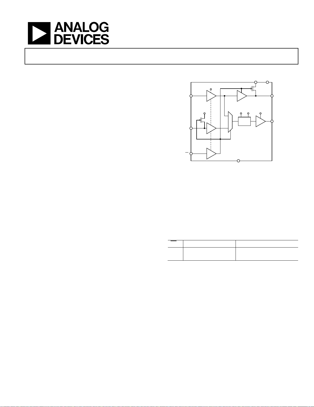
FUNCTIONAL BLOCK DIAGRAM
CC1VCC2
V
CC1
A1 Y1
V
CC1
A2
EN
PRODUCT HIGHLIGHTS
1. Bidirectional level translation matches any voltage level
from 1.65 V to 3.6 V.
2. The bypass switch offers high performance and is fully
guaranteed across the supply range.
3. Short circuit protection.
4. Tiny 8-lead SOT-23 package and 8-lead MSOP.
Table 1. Truth Table
EN
Signal Path Function
L
A1 → Y2, Y1 → V
H
A1 → Y2, A2 → Y2
CC1
V
V
CC1
0
1
GND
Figure 1.
Enable bypass mode
Enable normal mode
CC2VCC2
ADG3233
Y2
03297-001
Rev. A
Information furnished by Analog Devices is believed to be accurate and reliable. However, no
responsibility is assumed by Analog Devices for its use, nor for any infringements of patents or other
rights of third parties that may result from its use. Specifications subject to change without notice. No
license is granted by implication or otherwise under any patent or patent rights of Analog Devices.
Trademarks and registered trademarks are the property of their respective owners.
One Technology Way, P.O. Box 9106, Norwood, MA 02062-9106, U.S.A.
Tel: 781.329.4700 www.analog.com
Fax: 781.461.3113 ©2003–2011 Analog Devices, Inc. All rights reserved.
Page 2

ADG3233
TABLE OF CONTENTS
Features .............................................................................................. 1
Applications ....................................................................................... 1
Functional Block Diagram .............................................................. 1
General Description ......................................................................... 1
Product Highlights ........................................................................... 1
Revision History ............................................................................... 2
Specifications ..................................................................................... 3
Test Waveforms ............................................................................. 5
Absolute Maximum Ratings ............................................................ 6
REVISION HISTORY
7/11—Rev. 0 to Rev. A
Changes to Patent Number, General Description Section, and
Product Highlights Section ............................................................. 1
Changes to V
→ Y1, Table 2 ............................................................................. 4
EN
Changes to Table 3 ............................................................................ 6
Updated Outline Dimensions ....................................................... 15
Changes to Ordering Guide .......................................................... 16
5/03—Revision 0: Initial Version
CC
= V
CC1
= V
= 2.5 V ± 0.2 V, ENABLE Time
CC2
ESD Caution...................................................................................6
Pin Configuration and Function Descriptions ..............................7
Typical Performance Characteristics ..............................................8
Theory of Operation ...................................................................... 13
A1 and EN Input ........................................................................ 13
Normal Operation ...................................................................... 13
Bypass Operation ....................................................................... 14
Outline Dimensions ....................................................................... 15
Ordering Guide .......................................................................... 16
Rev. A | Page 2 of 16
Page 3

ADG3233
SPECIFICATIONS
V
= V
CC1
= 1.65 V to 3.6 V, GND = 0 V, all specifications T
CC2
Table 2.
Parameter1 Symbol Test Conditions/Comments Min Typ2 Max Unit
LOGIC INPUTS/OUTPUTS3 V
Input High Voltage4 V
V
IH
V
V
Input Low Voltage4 VIL V
V
V
Output High Voltage (Y1) VOH I
I
I
I
I
I
Output Low Voltage (Y1) VOL I
I
I
I
I
I
LOGIC OUTPUTS3 V
Output High Voltage (Y2) VOH I
I
I
I
I
I
Output Low Voltage (Y2) VOL I
I
I
I
I
I
SWITCHING CHARACTERISTICS
VCC = V
CC1
= V
= 3.3 V ± 0.3 V
CC2
4, 5
CC2
CC1
CC1
CC1
CC1
CC1
CC1
= −100 μA, V
OH
= −100 μA, V
OH
= −100 μA, V
OH
= −4 mA, V
OH
= −4 mA, V
OH
= −8 mA, V
OH
= 100 μA, V
OL
= 100 μA, V
OL
= 100 μA, V
OL
= 4 mA, V
OL
= 4 mA, V
OL
= 8 mA, V
OL
CC1
= −100 μA, V
OH
= −100 μA, V
OH
= −100 μA, V
OH
= −4 mA, V
OH
= −4 mA,V
OH
= −8 mA, V
OH
= 100 μA, V
OL
= 100 μA, V
OL
= 100 μA, V
OL
= 4 mA, V
OL
= 4 mA, V
OL
= 8 mA, V
OL
Propagation Delay, tPD
t
, t
CL = 30 pF, VT = VCC/2 3.5 5.4 ns
PHL
A1 → Y1 Normal Mode
A2 →Y2 Normal Mode
A1 → Y2 Bypass Mode
ENABLE Time EN → Y1
DISABLE Time EN → Y1
ENABLE Time EN → Y2
DISABLE Time EN → Y2
PLH
t
, t
CL = 30 pF, VT = VCC/2 3.5 5.4 ns
PHL
PLH
, t
CL = 30 pF, VT = VCC/2 4 6.5 ns
t
PHL
PLH
C
t
EN
t
C
DIS
t
C
EN
t
C
DIS
= 30 pF, VT = VCC/2 4 6 ns
L
= 30 pF, VT = VCC/2 2.8 4 ns
L
= 30 pF, VT = VCC/2 4.5 6.5 ns
L
= 30 pF, VT = VCC/2 4 6.5 ns
L
MIN
to T
, unless otherwise noted.
MAX
= 1.65 V to 3.6 V, GND = 0 V
= 3.0 V to 3.6 V 1.35 V
= 2.3 V to 2.7 V 1.35 V
= 1.65 V to 1.95 V 0.65 × VCC V
= 3.0 V to 3.6 V 0.8 V
= 2.3 V to 2.7 V 0.7 V
= 1.65 V to 1.95 V 0.35 × VCC V
= 3.0 V to 3.6 V 2.4 V
CC1
= 2.3 V to 2.7 V 2.0 V
CC1
= 1.65 V to 1.95 V VCC − 0.45 V
CC1
= 2.3 V to 2.7 V 2.0 V
CC1
= 1.65 V to 1.95 V VCC – 0.45 V
CC1
= 3.0 V to 3.6 V 2.4 V
CC1
= 3.0 V to 3.6 V 0.40 V
CC1
= 2.3 V to 2.7 V 0.40 V
CC1
= 1.65 V to 1.95 V 0.45 V
CC1
= 2.3 V to 2.7 V 0.40 V
CC1
= 1.65 V to 1.95 V 0.45 V
CC1
= 3.0 V to 3.6 V 0.40 V
CC1
= 1.65 V to 3.6 V, GND = 0 V
= 3.0 V to 3.6 V 2.4 V
CC2
= 2.3 V to 2.7 V 2.0 V
CC2
= 1.65 V to 1.95 V VCC − 0.45 V
CC2
= 2.3 V to 2.7 V 2.0 V
CC2
= 1.65 V to 1.95 V VCC – 0.45 V
CC2
= 3.0 V to 3.6 V 2.4 V
CC2
= 3.0 V to 3.6 V 0.40 V
CC2
= 2.3 V to 2.7 V 0.40 V
CC2
= 1.65 V to 1.95 V 0.45 V
CC2
= 2.3 V to 2.7 V 0.40 V
CC2
= 1.65 V to 1.95 V 0.45 V
CC2
= 3.0 V to 3.6 V 0.40 V
CC2
Rev. A | Page 3 of 16
Page 4
ADG3233
Parameter1 Symbol Test Conditions/Comments Min Typ2 Max Unit
VCC = V
VCC = V
Input Leakage Current II 0 ≤ VIN ≤ 3.6 V ±1 μA
Output Leakage Current IO 0 ≤ VIN ≤ 3.6 V ±1 μA
POWER REQUIREMENTS
Power Supply Voltages V
V
Quiescent Power Supply Current I
I
Increase in ICC per Input ΔI
1
Temperature range is as follows: B Version: −40°C to +85°C.
2
All typical values are at VCC = V
3
VIL and VIH levels are specified with respect to V
V
CC2
4
Guaranteed by design, not subject to production test.
5
See the Test Waveforms section.
= V
CC1
= 2.5 V ± 0.2 V
CC2
Propagation Delay, tPD
t
, t
CL = 30 pF, VT = VCC/2 4.5 6.2 ns
PHL
A1 → Y1 Normal Mode
A2 → Y2 Normal Mode
A1 → Y2 Bypass Mode
ENABLE Time EN → Y1
DISABLE Time EN → Y1
ENABLE Time EN → Y2
DISABLE Time EN → Y2
= V
CC1
= 1.8 V ± 0.15 V
CC2
PLH
t
, t
CL = 30 pF, VT = VCC/2 4.5 6.2 ns
PHL
PLH
t
, t
CL = 30 pF, VT = VCC/2 4.5 6.5 ns
PHL
PLH
tEN C
t
C
DIS
tEN C
t
C
DIS
= 30 pF, VT = VCC/2 5 7.2 ns
L
= 30 pF, VT = VCC/2 3.2 4.7 ns
L
= 30 pF, VT = VCC/2 5 7.7 ns
L
= 30 pF, VT = VCC/2 4.8 7.2 ns
L
Propagation Delay, tPD
t
, t
CL = 30 pF, VT = VCC/2 6.7 10 ns
PHL
A1 → Y1 Normal Mode
A2 → Y2 Normal Mode
A1 → Y2 Bypass Mode
ENABLE Time EN → Y1
DISABLE Time EN → Y1
ENABLE Time EN → Y2
DISABLE Time EN → Y2
.
= V
, TA = 25°C, unless otherwise stated.
CC1
CC2
PLH
t
, t
CL = 30 pF, VT = VCC/2 6.5 10 ns
PHL
PLH
, t
CL = 30 pF, VT = VCC/2 6.5 10.25 ns
t
PHL
PLH
tEN C
t
C
DIS
tEN C
t
C
DIS
1.65 3.6 V
CC1
1.65 3.6 V
CC2
Digital inputs = 0 V or VCC 2 μA
CC1
Digital inputs = 0 V or VCC 2 μA
CC2
CC1
, VOH, and VOL levels for Y1 are specified with respect to V
CC1
= 30 pF, VT = VCC/2 7 10.5 ns
L
= 30 pF, VT = VCC/2 4.4 6.5 ns
L
= 30 pF, VT = VCC/2 7 12 ns
L
= 30 pF, VT = VCC/2 6.5 10.5 ns
L
= 3.6 V, one input at 3.0 V; others at
V
CC
or GND
V
CC
, and VOH, and VOL levels are specified for Y2 with respect to
CC1
0.75 μA
Rev. A | Page 4 of 16
Page 5
ADG3233
V
V
V
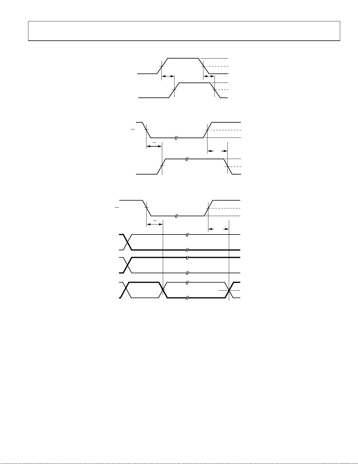
TEST WAVEFORMS
DIS
CC1
V
T
0V
V
OH
V
T
V
OL
03297-032
CC1
V
T
0V
V
OH
V
T
V
OL
03297-033
CC1
V
T
0V
V
CC1
0V
V
CC1
0V
V
OLH
V
T
V
OL
03297-034
INPUT
t
PHL
OUTPUT
t
PLH
Figure 2. Propagation Delay
EN
t
EN
t
DIS
Y1
(A1 AT GND)
V
T
Figure 3. Y1 Enable and Disable Times
EN
t
EN
t
A1
A2
V
Y2
Figure 4. Y2 Enable and Disable Times
T
Rev. A | Page 5 of 16
Page 6

ADG3233
ABSOLUTE MAXIMUM RATINGS
TA = 25°C, unless otherwise noted.
Table 3.
Parameter Rating
VCC to GND –0.3 V to +4.6 V
Digital Inputs to GND –0.3 V to +4.6 V
A1, EN
A2 –0.3 V to V
DC Output Current 25 mA
Operating Temperature Range
Industrial (B Version) –40°C to +85°C
Storage Temperature Range –65°C to +150°C
Junction Temperature 150°C
8-Lead MSOP
θJA Thermal Impedance 206°C/W
θJC Thermal Impedance 43°C/W
8-Lead SOT-23
θJA Thermal Impedance 211°C/W
Lead Temperature, Soldering (10 sec) 300°C
IR Reflow, Peak Temperature (<20 sec) 235°C
Soldering (Pb-Free)
Reflow, Peak Temperature 260(+0/−5)°C
Time at Peak Temperature 20 sec to 40 sec
–0.3 V to +4.6 V
+ 0.3 V
CC1
Stresses above those listed under Absolute Maximum Ratings
may cause permanent damage to the device. This is a stress
rating only; functional operation of the device at these or any
other conditions above those indicated in the operational
section of this specification is not implied. Exposure to absolute
maximum rating conditions for extended periods may affect
device reliability.
Only one absolute maximum rating may be applied at any one
time.
ESD CAUTION
Rev. A | Page 6 of 16
Page 7

ADG3233
PIN CONFIGURATION AND FUNCTION DESCRIPTIONS
V
CC1
A1
A2
EN
1
2
ADG3233
TOP VIEW
3
(Not to Scale)
4
V
8
CC2
Y1
7
6
Y2
GND
5
Figure 5. 8-Lead SOT-23 Package (RJ-8)
Table 4. Pin Function Descriptions
Pin No.
RJ-8 RM-8 Mnemonic Description
1 8 V
8 1 V
2 7 A1
3 6 A2
7 2 Y1
6 3 Y2
Supply Voltage 1, can be any supply voltage from 1.65 V to 3.6 V.
CC1
Supply Voltage 2, can be any supply voltage from 1.65 V to 3.6 V.
CC2
Input Referred to V
Input Referred to V
Output Referred to V
Output Referred to V
voltage level.
4 5
EN
Active Low Device Enable. When low, bypass mode is enabled; when high, the device is in normal mode.
5 4 GND Device Ground.
V
1
CC2
ADG3233
Y1
2
TOP VIEW
3
Y2
(Not to Scale)
4
03297-002
GND
V
8
CC1
A1
7
6
A2
5
EN
03297-003
Figure 6. 8-Lead MSOP Package (RM-8)
.
CC1
.
CC2
.
CC1
. Voltage levels appearing at Y2 will be translated from a V
CC2
voltage level to a V
CC1
CC2
Rev. A | Page 7 of 16
Page 8

ADG3233
TYPICAL PERFORMANCE CHARACTERISTICS
5.0
TA = 25°C
4.5
4.0
3.5
3.0
(nA)
2.5
CC1
I
2.0
1.5
1.0
0.5
0
1.5 2.0 2.5 3.0
= 2.5V
V
CC2
V
= 1.8V
CC2
Figure 7. I
V
= 3.3V
CC2
3.5 4.0
03297-004
(V)
V
CC1
vs. V
CC1
CC1
30
V
= 3.3V
CC1
25
20
15
(nA)
CC2
10
I
5
0
–5
0 1020304050607080
TEMPERATURE (°C)
Figure 10. I
CC2
V
= 3.3V
CC2
V
= 2.5V
CC2
V
= 1.8V
CC2
vs. Temperature
03297-007
5.0
TA = 25°C
4.5
4.0
3.5
3.0
(nA)
2.5
CC2
I
2.0
1.5
1.0
0.5
0
1.5 2.0 2.5 3.0
V
= 3.3V
CC1
Figure 8. I
30
V
= 3.3V
CC2
25
20
(nA)
15
CC1
I
10
5
2000
TA = 25°C
1800
1600
V
= V
1400
1200
(µA)
1000
CC1
I
800
= 2.5V
V
CC1
V
= 1.8V
CC1
= 3.3V
= 2.5V
= 1.8V
3.5 4.0
03297-005
(V)
V
CC2
vs. V
CC2
CC2
V
CC1
V
CC1
V
CC1
600
400
200
0
10k 100k 1M 10M 100M
Figure 11. I
80
TA = 25°C
70
60
50
(µA)
40
CC1
I
30
20
10
CC1
V
CC1
vs. Frequency, Normal Mode
CC1
= 3.3V
CC2
= V
= 1.8V
CC2
FREQUENCY (Hz)
V
= V
= V
CC2
CC2
= 3.3V
= 1.8V
CC1
V
CC1
03297-008
0
0 1020304050607080
TEMPERATURE (°C)
Figure 9. I
vs. Temperature
CC1
03297-006
Rev. A | Page 8 of 16
0
10k 100k 1M 10M 100M
Figure 12. I
FREQUENCY ( Hz)
vs. Frequency, Bypass Mode
CC1
03297-009
Page 9

ADG3233
2000
TA = 25°C
1800
1600
1400
1200
(µA)
1000
CC2
I
800
600
400
200
0
10k 100k 1M 10M 100M
Figure 13. I
V
=
C
C
1
V
= V
CC1
FREQUENCY (Hz)
vs. Frequency, Normal Mode
CC2
CC2
V
C
C
2
= 1.8V
3
V
3
=
.
03297-010
10
8
6
TIME (ns)
4
2
TA = 25°C
V
= V
CC1
0
1.5 2.0 2.5
CC2
Figure 16. Y2 Enable, Disable Time vs. Supply
t
DIS
t
EN
SUPPLY (V)
3.0 3.5 4.0
03297-013
2000
TA = 25°C
1800
1600
1400
1200
(µA)
1000
CC2
I
800
600
400
200
0
10k 100k 1M 10M 100M
Figure 14. I
10
8
6
TIME (ns)
4
t
V
3
=
=
.3
EN
C
C
2
= 1.8V
V
V
1
C
C
V
= V
CC1
CC2
FREQUENCY ( Hz)
vs. Frequency, Bypass Mode
CC2
t
DIS
6
5
t
= V
CC2
EN
t
DIS
= 3.3V
20 40 60 80
TEMPERATURE (°C)
03297-014
4
3
TIME (ns)
2
1
V
CC1
0
–40 –20 0
03297-011
Figure 17. Y1 Enable, Disable Time vs. Temperature
6
5
4
3
TIME (ns)
2
t
EN
t
DIS
2
TA = 25°C
V
= V
CC1
0
1.5 2.0 2.5
CC2
3.0 3.5 4.0
SUPPLY (V)
Figure 15. Y1 Enable, Disable Time vs. Supply
03297-012
Rev. A | Page 9 of 16
1
V
= V
CC2
= 3.3V
20 40 60 80
TEMPERATURE (°C)
CC1
0
–40 –20 0
Figure 18. Y2 Enable, Disable Time vs. Temperature
03297-015
Page 10

ADG3233
G
A
A
G
A
A
16
V
= 3.3V
CC1
V
= 1.8V
CC2
14
T
= 25°C
A
DATA RATE = 10Mbps
12
10
8
6
RISE/FALL TIME (ns)
4
2
0
22 32 52 6242
t
LOW-TO-HIGH T RANSITIO N
PLH,
t
HIGH-TO-LO W TRANSIT ION
PHL,
CAPACITIVE LOAD ( pF)
72 82 92 102
Figure 19. Rise/Fall Time vs. Capacitive Load, A1 → Y1, A2 → Y2
03297-016
10
V
= 1.8V
CC1
V
= 3.3V
9
CC2
T
= 25°C
A
DATA RATE = 10Mbps
8
7
t
LOW-TO-HIGH TRANSITION
6
5
4
RISE/FALL TIME (ns)
3
2
1
0
,
PLH
22 32 52 6242
t
HIGH-TO-LOW TRANSITION
,
PHL
CAPACITIVE LOAD ( pF)
72 82 92 102
Figure 22. Rise/Fall Time vs. Capacitive Load, A1 → Y2, Bypass Mode
03297-019
16
V
= 3.3V
CC1
V
= 1.8V
CC2
14
T
= 25°C
A
DATA RATE = 10Mbps
12
10
8
6
RISE/FALL TIME (ns)
4
2
0
22 32 52 6242
t
t
LOW-TO-HIGH TRANSITION
PLH,
HIGH-TO-LO W TRANSIT ION
PHL,
CAPACITIVE LOAD ( pF)
72 82 92 102
Figure 20. Rise/Fall Time vs. Capacitive Load, A1 → Y2, Bypass Mode
10
V
= 1.8V
CC1
V
= 3.3V
9
CC2
T
= 25°C
A
DATA RATE = 10Mbps
8
7
t
LOW-TO-HIGH T RANSITIO N
,
6
PLH
5
4
RISE/FALL TIME (ns)
3
2
1
0
22 32 52 6242
t
HIGH-TO-LOW TRANSITION
,
PHL
CAPACITIVE LOAD ( pF)
72 82 92 102
Figure 21. Rise/Fall Time vs. Capacitive Load, A1 → Y1, A2 → Y2
8
V
= 3.3V
CC1
V
= 3.3V
CC2
7
T
= 25°C
A
DATA RATE = 10Mbps
6
Y (ns)
5
4
TION DEL
3
2
PROPA
1
0
22 32 52 6242
03297-017
t
LOW-TO-HIGH TRANSITION
,
PLH
t
PHL
CAPACITIVE LOAD (pF)
HIGH-TO-LO W TRANSIT ION
,
72 82 92 102
03297-020
Figure 23. Propagation Delay vs. Capacitive Load A1 → Y1
8
7
t
LOW-TO-HIGH TRANSI TION
,
= 3.3V
= 3.3V
= 25°C
PLH
t
PHL
CAPACITIVE LOAD (pF)
HIGH-TO-LO W TRANSIT ION
,
72 82 92 102
03297-021
6
Y (ns)
5
4
TION DEL
3
2
PROPA
V
CC1
V
CC2
1
T
A
DATA RATE = 10Mbps
0
03297-018
22 32 52 6242
Figure 24. Propagation Delay vs. Capacitive Load A2 → Y2
Rev. A | Page 10 of 16
Page 11

ADG3233
G
A
A
G
A
A
G
A
A
G
A
A
G
A
A
8
7
4.0
3.5
t
PHL
A2 → Y2
,
t
PHL
A1 → Y1
,
6
t
LOW-TO-HIGH T RANSITIO N
,
PLH
Y (ns)
5
t
HIGH-TO-LO W TRANSITION
4
TION DEL
PHL
,
3
2
PROPA
V
= 3.3V
CC1
V
= 3.3V
CC2
1
T
= 25°C
A
DATA RATE = 10Mbps
0
22 32 52 6242
CAPACITIVE LOAD (pF)
72 82 92 102
03297-022
Figure 25. Propagation Delay vs. Capacitive Load A1 → Y2, Bypass Mode
8
7
t
A1 → Y1
,
= V
t
PHL
A1 → Y1
,
CC2
PLH
t
A2 → Y2
,
PHL
t
PLH
SUPPLY (V)
A2 → Y2
,
4.0
03297-023
6
Y (ns)
5
4
TION DEL
3
2
PROPA
TA = 25°C
1
V
CC1
0
1.5 2.0 2.5 3. 0 3.5
Figure 26. Propagation Delay vs. Supply, Normal Mode
3.0
Y (ns)
2.5
t
A1 → Y1
t
A2 → Y2
,
2.0
TION DEL
PLH
PLH
,
1.5
1.0
PROPA
0.5
V
= V
CC2
= 3.3V
20 40 60 80
CC1
0
–40 –20 0
TEMPERATURE (°C)
Figure 28. Propagation Delay vs. Temperature, Normal Mode
4
t
A1 → Y2
,
PHL
3
t
PLH
A1 → Y2
,
Y (ns)
2
TION DEL
1
PROPA
V
= V
CC2
= 3.3V
20 40 60 80
CC1
0
–40 –20 0
TEMPERATURE (°C)
Figure 29. Propagation Delay vs. Temperature, Bypass Mode
03297-025
03297-026
8
6
Y (ns)
t
A1 → Y2
,
4
TION DEL
2
PROPA
TA = 25°C
V
= V
CC1
0
1.5 2.0 2.5 3.0 3. 5
CC2
PHL
t
PLH
A1 → Y2
,
SUPPLY (V)
Figure 27. Propagation Delay vs. Supply, Bypass Mode
4.0
03297-024
Rev. A | Page 11 of 16
T
= 25°C
A
EN = HIGH
3
1
2
4
CH1 1.00V CH2 500mV
CH3 1.00VΩ CH4 1.00VΩ
Figure 30. Normal Mode V
A1
Y1
A2
Y2
DATA RATE = 10MHz
M5.00ns CH1 1.48V
= 3.3 V, V
CC1
= 1.8 V
CC2
3.3V
1.8V
3.3V
03297-027
Page 12

ADG3233
T
= 25°C
A
DATA RATE = 10MHz
A1
Y2
3
2
CH2 1.00VΩ CH2 500mV M5.00ns CH2 1.47V
Figure 31. Bypass Mode, V
CC1
= 3.3 V, V
3.3V
1.8V
CC2
= 1.8 V
A1
3
2
Y1
1
CH1 1.00V CH2 2.00V
03297-028
CH3 1.00VΩ
Figure 33. Bypass Mode, V
Y2
M5.00ns CH3 900mV
= 1.8 V, V
CC1
1.8V
3.3V
1.8V
T
= 25°C
CC2
A
= 3.3 V
DATA RATE = 10MHz
03297-030
3
1
A2
4
2
CH1 1.00V CH2 2.00V
CH3 5.00VΩ CH4 1.00VΩ
Figure 32. Normal Mode, V
A1
Y1
Y2
DATA RATE = 10MHz
M5.00ns CH1 1.48V
= 1.8 V, V
CC1
T
CC2
3.3V
1.8V
1.8V
3.3V
= 25°C
A
= 3.3 V
3.5
3.0
2.5
2.0
1.5
VOLTAGE (V)
1.0
0.5
0
03297-029
05
VCC = 3.3V
VCC = 2.5V
VCC = 1.8V
VCC = 1.8V
SINK
10 15 20
CURRENT (mA)
VCC = 2.5V
TA = 25°C
VCC = V
SOURCE
CC1
V
CC
Figure 34. Y1 and Y2 Source and Sink Current
= V
= 3.3V
CC2
03297-031
Rev. A | Page 12 of 16
Page 13

ADG3233
V
V
V
THEORY OF OPERATION
The ADG3233 is a bypass switch designed on a submicron
process that operates from supplies as low as 1.65 V. The device
is guaranteed for operation over the supply range 1.65 V to 3.6 V. It
operates from two supply voltages, allowing bidirectional level
translation, that is, it translates low voltages to higher voltages
and vice versa. The signal path is unidirectional, meaning data
may only flow from A → Y.
A1 AND EN INPUT
The A1 and enable (EN) inputs have VIL/VIH logic levels so that
the part can accept logic levels of V
controlling device independent of the value of the supply being
used by the controlling device. These inputs (A1,
capable of accepting inputs outside the V
example, the V
supply applied to the bypass switch could be
CC1
1.8 V while Device 0 could be operating from a 2.5 V or 3.3 V
supply rail, there are no internal diodes to the supply rails, so
the device can handle inputs above the supply but inside the
absolute maximum ratings.
from Device 0 or the
OL/VOH
supply range. For
CC1
CC0
EN
) are
NORMAL OPERATION
Figure 35 shows the bypass switch being used in normal mode.
In this mode, the signal paths are from A1 → Y1 and A2 → Y2.
The device will level translate the signal applied to A1 to a V
logic level (this level translation can be either to a higher or
lower supply) and route the signal to the Y1 output, which
will have standard V
is then passed through Device 1 and back to the A2 input pin
of the bypass switch.
The logic level inputs of A2 are with respect to the V
The signal will be level translated from V
to the Y2 output pin of the bypass switch. Y2 output logic levels
are with respect to the V
CC1
OL/VOH
CC2
CC2
levels for V
supply.
supplies. The signal
CC1
to V
CC1
supply.
CC1
and routed
CC2
CC1
DEVICE 0 DEVICE 1 DEVICE 2
SIGNAL IN PUT
LOGIC 1
V
V
CC2
CC1
A1
A2
EN
BYPASS SWITCH
Figure 35. Bypass Switch in Normal Mode
Y1
Y2
SIGNAL OUTPUT
03297-035
Rev. A | Page 13 of 16
Page 14

ADG3233
V
V
V
BYPASS OPERATION
Figure 36 illustrates the device as used in bypass mode. The
signal path is now from A1 directly to Y2, thus bypassing
Device 1 completely. The signal will be level translated to a V
CC2
logic level and available on Y2, where it may be applied directly
to the input of Device 2. In bypass mode, Y1 is pulled up to V
CC1
.
CC0
The three supplies in Figure 35 and Figure 36 may be any
combination of supplies, that is., V
CC0
, V
CC1
, and V
any combination of supplies, for example, 1.8 V, 2.5 V, and 3.3 V.
CC1
CC2
may be
CC2
SIGNAL IN PUT
DEVICE 0 DEVICE 1
V
V
CC2
CC1
A1
A2
LOGIC 0
EN
BYPASS SWITCH
Y1
Y2
DEVICE 2
SIGNAL OUTPUT
03297-036
Figure 36. Bypass Switch in Bypass Mode
Rev. A | Page 14 of 16
Page 15

ADG3233
0
0
OUTLINE DIMENSIONS
3.20
3.00
2.80
8
5
3.20
3.00
2.80
PIN 1
IDENTIFIER
0.95
0.85
0.75
0.15
0.05
COPLANARITY
1
0.65 BSC
0.10
COMPLIANT TO JEDEC STANDARDS MO-187-AA
Figure 37. 8-Lead Mini Small Outline Package [MSOP]
3.00
2.90
2.80
5.15
4.90
4.65
4
15° MAX
6°
0°
0.23
0.09
0.40
0.25
1.10 MAX
(RM-8)
Dimensions shown in millimeters
0.80
0.55
0.40
10-07-2009-B
1.70
1.60
1.50
PIN 1
INDICATOR
1.30
1.15
0.90
.15 MAX
.05 MIN
8
1234
COMPLIANT TO JEDEC STANDARDS MO-178-BA
1.95
BSC
5
0.38 MAX
0.22 MIN
0.65 BSC
1.45 MAX
0.95 MIN
3.00
2.80
2.60
SEATING
PLANE
0.22 MAX
0.08 MIN
8°
0.60
4°
BSC
0°
0.60
0.45
0.30
12-16-2008-A
76
Figure 38. 8-Lead Small Outline Transistor Package [SOT-23]
(RJ-8)
Dimensions shown in millimeters
Rev. A | Page 15 of 16
Page 16

ADG3233
ORDERING GUIDE
Model1 Temperature Range Package Description Branding Package Option
ADG3233BRJ-REEL −40°C to +85°C 8-Lead SOT-23 W1B RJ-8
ADG3233BRJ-REEL7 −40°C to +85°C 8-Lead SOT-23 W1B RJ-8
ADG3233BRJZ-REEL7 −40°C to +85°C 8-Lead SOT-23 S1S RJ-8
ADG3233BRM −40°C to +85°C 8-Lead MSOP W1B RM-8
ADG3233BRM-REEL −40°C to +85°C 8-Lead MSOP W1B RM-8
ADG3233BRM-REEL7 −40°C to +85°C 8-Lead MSOP W1B RM-8
ADG3233BRMZ −40°C to +85°C 8-Lead MSOP S1S RM-8
ADG3233BRMZ-REEL7 −40°C to +85°C 8-Lead MSOP S1S RM-8
1
Z = RoHS Compliant Part.
©2003–2011 Analog Devices, Inc. All rights reserved. Trademarks and
registered trademarks are the property of their respective owners.
D03297-0-7/11(A)
Rev. A | Page 16 of 16
 Loading...