

Page 1
查询ADG3231供应商查询ADG3231供应商
Low Voltage, Single-Channel
Level Translator
FEATURES
Operates from 1.65 V to 3.6 V Supply Rails
Unidirectional Signal Path, Bidirectional Level Translation
Tiny 6-Lead SOT-23 Package
Short Circuit Protection
LV T TL/CMOS Compatible Inputs
APPLICATIONS
Level Translation
Low Voltage ASIC Translation
Serial Interface Translation
GENERAL DESCRIPTION
The ADG3231 is a level translator designed on a submicron
process that operates from supplies as low as 1.65 V. The device
is guaranteed for operation over the supply range 1.65 V to 3.6 V.
It operates from two supply voltages, allowing bidirectional level
translation, i.e., it translates low voltages to higher voltages and
vice versa. The signal path is unidirectional, meaning data may
fl ow only from A1 to Y1.
This type of device may be used in applications requiring communication between devices operating from different supply levels.
The level translator is packaged in one of the smallest footprints
available for its pin count. The 6-lead SOT-23 package requires
only a maximum of 5.28 mm ⫻ 5.28 mm board space.
ADG3231
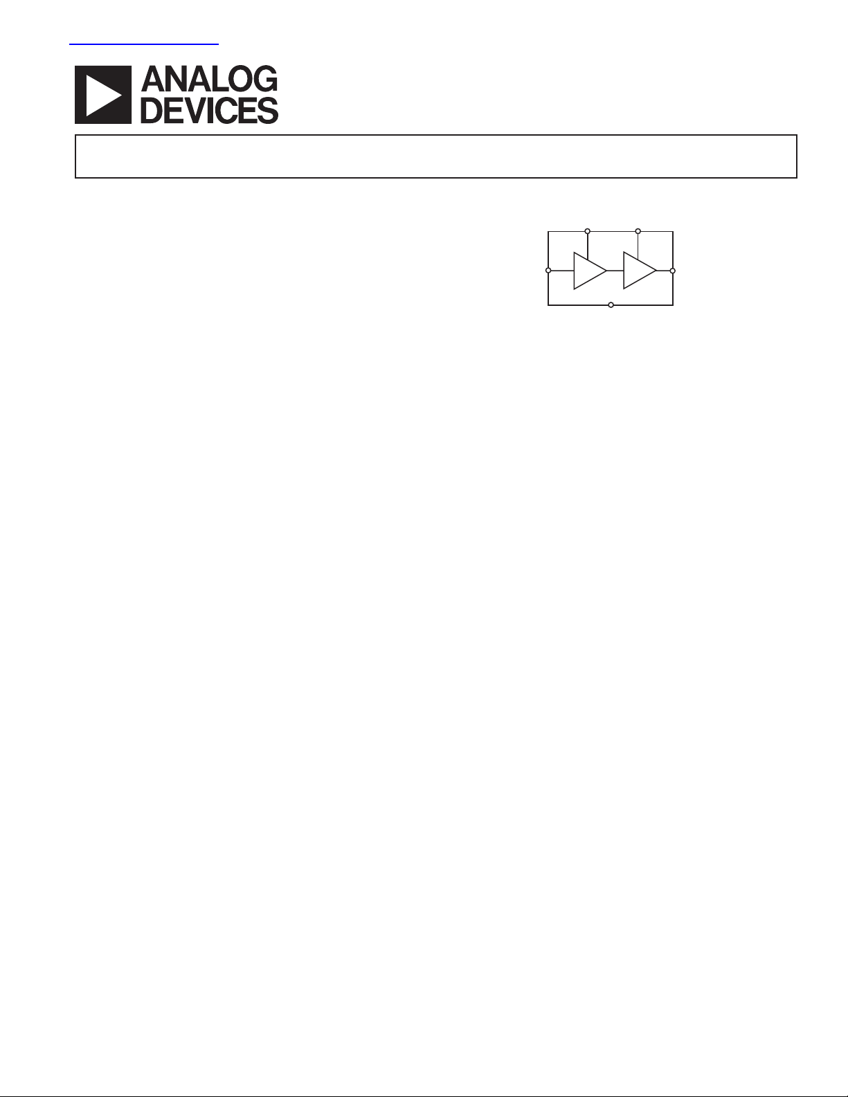
FUNCTIONAL BLOCK DIAGRAM
V
CC1
A1
PRODUCT HIGHLIGHTS
1. Bidirectional level translation matches any voltage level from
1.65 V to 3.6 V.
2. The device offers high performance and is fully guaranteed
across the supply range.
3. Short circuit protection.
4. Tiny SOT-23 package.
GND
V
CC2
Y1
*
*Patent Pending
REV. 0
Information furnished by Analog Devices is be lieved to be accurate and
reliable. However, no responsibility is assumed by Analog Devices for its
use, nor for any infringements of patents or other rights of third parties
that may result from its use. No license is granted by implication or otherwise under any patent or patent rights of Analog Devices. Trademarks
and registered trademarks are the property of their respective companies.
One Technology Way, P.O. Box 9106, Norwood, MA 02062-9106, U.S.A.
Tel: 781/329-4700 www.analog.com
Fax: 781/326-8703 © 2003 Analog Devices, Inc. All rights reserved.
Page 2

(V
= V
ADG3231–SPECIFICATIONS
CC1
1
oth er wise noted.)
= 1.65 V to 3.6 V, GND = 0 V. All specifi cations T
CC2
MIN
to T
, un less
MAX
Parameter Symbol Conditions Min Typ2 Max Unit
LOGIC INPUTS/OUTPUTS
Input High Voltage4 VIH V
V
V
Input Low Voltage
4
VIL V
V
V
Output High Voltage V
V
V
I
V
I
Output Low Voltage V
V
V
I
V
I
SWITCHING CHARACTERISTICS
Propagation Delay, tPD A1 to Y1 t
Propagation Delay, t
Propagation Delay, t
PD
PD
Input Leakage Current I
Output Leakage Current I
3
4, 5
A1 to Y1 t
A1 to Y1 t
= 3.0 V to 3.6 V 1.35 V
V
IH
V
IH
V
IL
V
IL
IOH = –100 µA, V
OH
IOH = +100 µA, V
OL
, t
PHL
, t
PHL
, t
PHL
0 ⱕ VIN ⱕ 3.6 V ±1 µA
I
O
CC1
= 2.3 V to 2.7 V 1.35 V
CC1
= 1.65 V to 1.95 V 0.65 VCC V
CC1
= 3.0 V to 3.6 V 0.8 V
CC1
= 2.3 V to 2.7 V 0.7 V
CC1
= 1.65 V to 1.95 V 0.35 VCC V
CC1
= –4 mA, V
OH
= –8 mA, V
OH
= +4 mA, V
OH
= +8 mA, V
OH
3.3 V ± 0.3 V, CL = 30 pF, VT = VCC/2 4 6.5 ns
PLH
2.5 V ± 0.2 V, CL = 30 pF, VT = VCC/2 4.5 6.5 ns
PLH
1.8 V ± 0.15 V, CL = 30 pF, VT = VCC/2 6.5 10.25 ns
PLH
= 3.0 V to 3.6 V 2.4 V
CC2
= 2.3 V to 2.7 V 2.0 V
CC2
= 1.65 V to 1.95 V VCC – 0.45 V
CC2
= 2.3 V to 2.7 V 2.0 V
CC2
= 1.65 V to 1.95 V VCC – 0.45 V
CC2
= 3.0 V to 3.6 V 2.4 V
CC2
= 3.0 V to 3.6 V 0.4 V
CC2
= 2.3 V to 2.7 V 0.4 V
CC2
= 1.65 V to 1.95 V 0.45 V
CC2
= 2.3 V to 2.7 V 0.4 V
CC2
= 1.65 V to 1.95 V 0.45 V
CC2
= 3.0 V to 3.6 V 0.4 V
CC2
0 ⱕ VIN ⱕ 3.6 V ±1 µA
POWER REQUIREMENTS
Power Supply Voltages V
V
Quiescent Power Supply Current I
I
NOTES
1
Temperature range is as follows: B Version: –40°C to +85°C.
2
All typical values are at V
3
VIL and VIH levels are specifi ed with respect to V
4
Guaranteed by design, not subject to production test.
5
See Test Circuit and Waveforms.
Specifi cations subject to change without notice.
CC1
= V
, TA = 25°C, unless otherwise stated.
CC2
CC1
1.65 3.6 V
CC1
1.65 3.6 V
CC2
Digital Inputs = 0 V or VCC 2 µA
CC1
Digital Inputs = 0 V or VCC 2 µA
CC2
; VOH and VOL levels are with respect to V
CC2
.
–2–
REV. 0
Page 3
ADG3231
ABSOLUTE MAXIMUM RATINGS*
(TA = 25°C, unless otherwise noted.)
VCC to GND . . . . . . . . . . . . . . . . . . . . . . . . . . –0.3 V to +4.6 V
A1 Input Voltage . . . . . . . . . . . . . . . . . . . –0.3 V to V
CC1
+0.3 V
DC Output Current . . . . . . . . . . . . . . . . . . . . . . . . . . . 25 mA
Operating Temperature Range
Industrial (B Version) . . . . . . . . . . . . . . . . . . –40°C to +85°C
Storage Temperature Range . . . . . . . . . . . . . –65°C to +150°C
Junction Temperature . . . . . . . . . . . . . . . . . . . . . . . . . . . .150°C
6-Lead SOT-23,
Thermal Impedance . . . . . . . . . . . . . . . . . . . . . 229°C/W
q
JA
Lead Temperature, Soldering (10 seconds) . . . . . . . . . . . 300°C
IR Refl ow, Peak Temperature (<20 seconds) . . . . . . . . . . 235°C
*Stresses above those listed under Absolute Maximum Ratings may cause permanent
damage to the device. This is a stress rating only; functional operation of the device
at these or any other conditions above those listed in the operational sections of this
specification is not implied. Exposure to absolute maximum rating conditions for
extended periods may affect device reliability. Only one absolute maximum rating
may be applied at any one time.
ORDERING GUIDE
Model Temperature Range Package Description Branding Package Option
ADG3231BRJ-REEL –40°C to +85°C SOT-23 W2B RJ-6
ADG3231BRJ-REEL7 –40°C to +85°C SOT-23 W2B RJ-6
PIN CONFIGURATION
V
V
CC1
NC
A1
1
ADG3231
2
(No t to Scale)
3
6
CC2
Y1
5
GND
4
PIN FUNCTION DESCRIPTIONS
Pin Mnemonic Description
1 V
CC1
Supply Voltage 1, can be any supply voltage from 1.65 V to 3.6 V.
2 NC Not Internally Connected.
3 A1
Digital Input Referred to V
CC1
.
4 GND Device Ground Pin.
5 Y1
6 V
CC2
Digital Output Referred to V
Supply Voltage 2, can be any supply voltage from 1.65 V to 3.6 V.
CC2
.
CAUTION
ESD (electrostatic discharge) sensitive device. Electrostatic charges as high as 4000 V readily ac cu mu late
on the human body and test equipment and can discharge without detection. Although the ADG3231
features proprietary ESD pro tec tion circuitry, permanent damage may occur on devices subjected to high
energy electrostatic discharges. Therefore, proper ESD pre cau tions are rec om mend ed to avoid per for mance
deg ra da tion or loss of functionality.
REV. 0
–3–
Page 4

ADG3231–Typical Performance Characteristics
5.0
TA = 25ⴗC
4.5
4.0
3.5
3.0
2.5
– nA
CC1
2.0
I
1.5
V
1.0
0.5
0
1.5 2.0 3.02.5 3.5 4.0
V
= 2.5V
CC2
TPC 1. I
30
V
= 3.3V
CC1
= 25ⴗC
T
A
25
20
– nA
15
CC2
I
10
–5
5
0
08070605040302010
V
V
= 3.3V
CC2
= 1.8V
CC2
V
– V
CC1
vs. V
CC1
V
= 1.8V
CC2
TEMPERATURE – ⬚C
CC2
V
CC2
= 2.5V
CC1
= 3.3V
5.0
TA = 25ⴗC
4.5
4.0
3.5
3.0
– nA
2.5
CC2
I
2.0
1.5
V
= 3.3V
CC1
1.0
0.5
0
1.5 2.0 3.02.5 3.5 4.0
TPC 2. I
80
T
= 25ⴗC
A
70
60
50
40
– A
CC1
I
30
20
10
V
CC1
0
10k 100k 1M
V
= 2.5V
CC1
V
– V
CC2
vs. V
CC2
V
= V
CC1
= V
= 1.8V
CC2
FREQUENCY – Hz
V
CC1
CC2
= 3.3V
CC2
10M 100M
= 1.8V
30
25
20
– nA
15
CC1
I
10
5
0
08070605040302010
TPC 3. I
2000
1800
1600
1400
1200
1000
– A
CC2
I
800
600
400
200
0
10k 100k
T
V
CC2
T
A
= 25ⴗC
A
= 3.3V
= 25ⴗC
TEMPERATURE – ⬚C
vs. Temperature
CC1
V
CC1
V
V
=
CC1
FREQUENCY – Hz
= V
CC2
V
V
V
CC2
1M
CC1
CC1
CC1
= 3.3V
= 1.8V
= 3.3V
= 2.5V
= 1.8V
10M 100M
TPC 4. I
10
8
6
TIME – ns
4
2
TA = 25ⴗC
V
CC1
0
1.5 2.0 3.02.5 3.5 4.0
vs. Temperature
CC2
= V
CC2
SUPPLY – V
t
EN
t
DIS
TPC 7. Enable, Disable Time vs. Supply
TPC 5. I
6
5
4
3
TIME – ns
2
1
V
CC1
0
–40 –20 200408060
vs. Frequency
CC1
t
EN
t
DIS
= V
3.3V
CC2 =
TEMPERATURE – ⴗC
TPC 8. Enable, Disable
vs. Temperature
Time
TPC 6. I
16
V
= 3.3V
CC1
= 1.8V
V
CC2
14
= 25ⴗC
T
A
DATA RATE 10Mbps
12
10
8
6
RISE/FALL TIME – ns
4
2
0
22 10292827262524232
vs. Frequency
CC2
t
, LOW-TO-HIGH TRANSITION
PLH
t
, HIGH-TO-LOW TRANSITION
PHL
CAPACITIVE LOAD – pF
TPC 9. Rise/Fall Time vs.
Capacitive Load, A1–Y1
–4–
REV. 0
Page 5

ADG3231
10
V
= 1.8V
CC1
9
= 3.3V
V
CC2
= 25ⴗC
T
A
8
DATA RATE 10Mbps
t
, LOW-TO-HIGH TRANSITION
LH
7
6
5
4
3
RISE/FALL TIME – ns
2
t
, HIGH-TO-LOW TRANSITION
HL
1
0
22 10292827262524232
CAPACITIVE LOAD – pF
TPC 10. Rise/Fall Time vs.
Capacitive Load, A1–Y1
4.0
t
, A1–Y2
PHL
3.0
2.0
1.0
PROPAGATION DELAY – ns
TA = 25ⴗC
V
CC1
0
t
PLH
= V
= 3.3V
CC2
TEMPERATURE – ⴗC
, A1–Y2
8
V
= 3.3V
CC1
= 3.3V
V
CC2
7
= 25ⴗC
T
A
DATA RATE 10Mbps
6
t
, LOW-TO-HIGH TRANSITION
PLH
5
4
t
, HIGH-TO-LOW TRANSITION
3
2
PROPAGATION DELAY – ns
1
0
22 10292827262524232
PHL
CAPACITIVE LOAD – pF
TPC 11. Propagation Delay
vs. Capacitive Load, A1–Y1
TA = 25ⴗC
DATA RATE = 10MHz
A1
3
2
806040200–20–40
3.3V
1.8V
Y1
8.0
6.0
t
, A1–Y2
= V
PHL
CC2
t
, A1–Y2
PLH
SUPPLY – V
4.0
2.0
PROPAGATION DELAY – ns
TA = 25ⴗC
V
CC1
0
1.5 2.0 3.02.5 3.5 4.0
TPC 12. Propagation Delay
vs. Supply, Bypass Mode
A1
3
2
1
1.8V
Y2
TA = 25ⴗC
DATA RATE = 10MHz
3.3V
TPC 13 Propagation Delay
vs. Temperature
3.5
3
2.5
VCC = 2.5V
2
1.5
VCC = 1.8V
VOLTAGE – V
1
VCC = 1.8V
0.5
SINK
0
02015105
VCC = 3.3V
TA = 25ⴗC
V
CC = VCC1
VCC = 2.5V
CURRENT – mA
SOURCE
VCC = 3.3V
= V
CC2
TPC 16. Y1 Sink and Source Current
TPC 14. Input/Output
V
= 3.3 V, V
CC1
CC2
= 1.8 V
TPC 15. Input/Output
V
= 1.8 V, V
CC1
= 3.3 V
CC2
REV. 0
–5–
Page 6

ADG3231
TEST CIRCUIT
V
INPUT
OUTPUT
t
t
PLH
PHL
CC1
V
T
0V
V
OH
V
L
V
OL
Figure 1. Propagation Delay
DESCRIPTION
The ADG3231 is a level translating device designed on a submicron
process that operates from supplies as low as 1.65 V. The device is
guaranteed for operation over the supply range 1.65 V to 3.6 V.
It operates from two supply voltages, allowing bidirectional level
translation, i.e., it translates low voltages to high voltages and vice
versa. The signal path is unidirectional, meaning data may only
fl ow from A to Z.
SIGNAL INPUT
V
CC1
DEVICE 1
V
CC1
A1
ADG3231
GND
A1 Input
The A1 input is capable of accepting inputs outside the V
range. For example, the V
supply applied to the device could
CC1
CC1
supply
be 1.8 V while the preceding device could be supplied from a 2.5 V or
3.3 V supply rail. There are no internal diodes to the supply rails,
so the ADG3231 can handle inputs above the supply but inside
the absolute maximum ratings stated.
Normal Operation
The signal path is from A1 to Y1. The device will level translate
the signal applied to A1 to a V
logic level (this level translation
CC1
can be to either a higher or a lower supply) and route the signal
to the Y1 output, which will have standard V
supplies.
V
CC2
The supplies in Figure 2 may be any combination of
e.g., V
CC1
and V
may be anywhere in the range of 1.65 V to
CC2
OL/VOH
levels for
supplies,
3.6 V.
V
CC2
Y1
VCC2
DEVICE 2
SIGNAL OUTPUT
Figure 2. Typical Operation of the ADG3231 Level Translating Switch
–6–
REV. 0
Page 7

OUTLINE DIMENSIONS
6-Lead Small Outline Transistor Package [SOT-23]
(RJ-6)
Dimensions shown in millimeters
2.90 BSC
ADG3231
1.60 BSC
1.30
1.15
0.90
0.15 MAX
2
1.90
BSC
0.50
0.30
4 5
0.95 BSC
2.80 BSC
1.45 MAX
SEATING
PLANE
6
1 3
PIN 1
COMPLIANT TO JEDEC STANDARDS MO-178AB
0.22
0.08
10ⴗ
0.60
4ⴗ
0.45
0ⴗ
0.30
REV. 0
–7–
Page 8

C03298–0–5/03(0)
–8–
 Loading...